

Page 1
MT88V32
8 x 4 High Performance Video Switch Array
Preliminary Information
Features
• 32 bidirectional CMOS "T" switches in an 8×4
non-blocki ng arra y
• Break-before-make switching configuration
• Fast setup & hold times for switch programming
• 3dB bandwidth of 200MHz
• Low fee dt h ro ug h an d cro s st al k, be tt e r tha n -80 dB
at 5MHz
• Very low differential gain a nd phase erro rs
• 12Vpp bipolar signal capability
• On-state resistance 7 5Ω (max) fo r V
=-7V
V
EE
DD
=+5V,
• Switch control through 2-stage latches
• Orthog onal Xi and Yi pin conne ctio ns for
optimize d PCB l ayo ut
• Latch readback capability for monitoring
Applications
• High-e nd vide o rout ing an d switc hing
• Medical inst rumen tation
• Automa tic t est eq uipmen t (ATE)
• Multi-m ed ia communica tion
Description
The MT88V32 is a digitally programmable (TTL levels)
8
×4 crosspoint switch that is designed to control wide-
band analog (video) signal.
ISSUE 1 August 1993
Ordering Information
MT88V32A P 44 Pin PLCC
-40° to 85°C
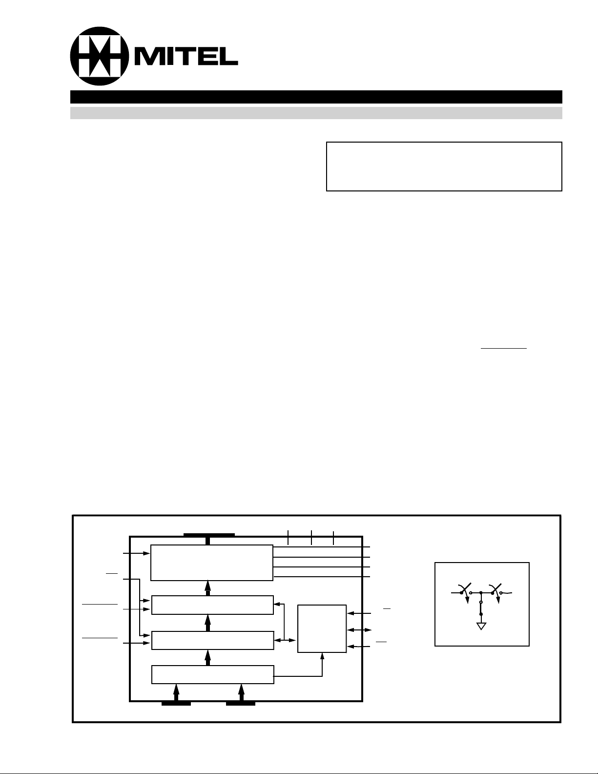
Each of the 32 nodes of the switching matrix has a Tswitch, see Fig.1. This grounds the nodes of all open
connections, which greatly reduces feedthrough
noise. In order to reduce crosstalk, individual analog
signal lines are isolated by interleaving them with
ground lines.
The two stage programmable latch system allows
the state of all switching nodes to be updated
simultaneously. The next state of the switch is written
into the first stage of the latches through individual
write cycles. These changes will not affect the
current state of the switch. The STROBE2
control
input is used to load the state of all first st age latches
to the second stage latches, which updates the
complete matrix. Therefore, all 32 switching nodes
are updated simultaneously.
The MT88V32 supports separate analog (V
digi tal (V
) voltage references. This allows the user
DD
EE
) and
to select an optimum analog signal bias point.
GND
MR
STROBE2
STROBE1
Y0-Y7 VDD VSS
"T" Switch Array
2nd Stage Latches
1st Stage Latches
Address Decode
AX0-AX1
8x4
VEE
X0
X1
X2
X3
I/O
Control
Logic
AY0-AY2
R/W
DATA
CS
Figure 1 - Functional Block Diagram
Yi
GND
T-Switch Configuration
Xi
3-51
Page 2
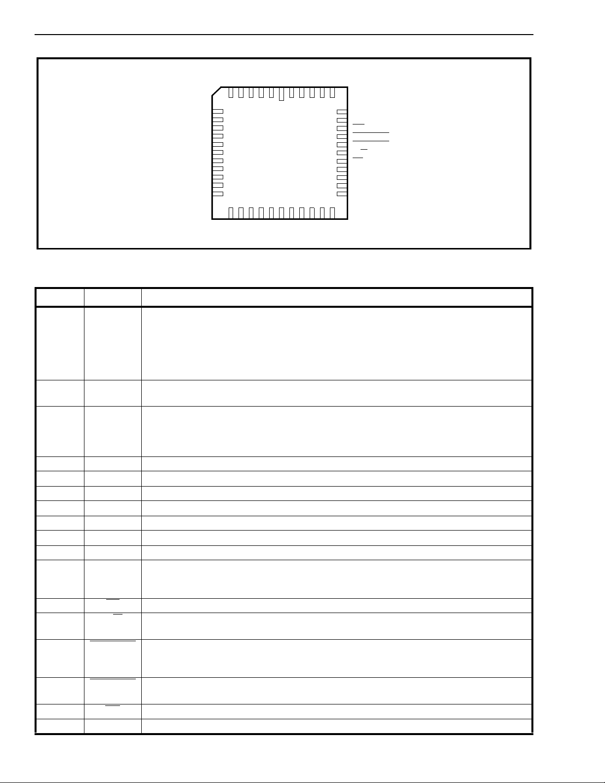
MT88V32 Preliminary Information
X3
GND
X2
GND
X1
GND
X0
GND
GND
Y0
GND
40
39
GND
38
NC
37
MR
36
STROBE2
35
STROBE1
34
R/W
33
CS
32
DATA
31
AY0
30
AY1
29
NC
AX1
NC
AX0
AY2
* Connects toV
EE
Y1
GND
Y2
GND
Y3
GND
Y4
GND
Y5
GND
Y6
6 5 4 3 2 44434241
7
8
9
10
11
12
13
14
15
16
17
GNDY7GND
1
23181920 2122 2425262728
IC*
VEE
VDD
VSS
Figure 2 - Pin Conne ctions
Pin Description
Pin #* Name Description
1, 3, 4, 6,
8, 10,
12, 14,
16, 18,
20, 39,
41, 43
2, 44,
42, 40
5, 7,
9, 11,
13, 15,
17, 19
21 V
22 IC Internal Connection.
23 V
24 V
25, 26 AX1,AX0 X0-X3 I/O Address Select (inputs).
27, 30,31 AY2-AY0 Y0-Y7 I/O Address Sele ct (inp uts).
28, 29 NC No Connection.
32 DATA DATA (input/output). When input, a logic high will close the selected switch and a logic
33 CS
34 R/W
35 STROBE1
36 STROBE2
37 MR
38 NC No Connection.
GND Analog Ground. Connect to system ground for crosstalk noise isolation. Pins 3 and 39
are not bonded internally.
X0, X1,
Analog Lines (input/output).
X2, X3
Y0, Y1,
Analog Lines (input/output).
Y2, Y3
Y4, Y5,
Y6, Y7
EE
DD
SS
Negative Analog Power Supply.
Positive Po wer Supply.
Digital Ground Reference.
low will open the selected switch. When output , a logic high indicate s a closed switch
and a logic low indicates an opened switch.
Chip Select (input). Active low.
READ/WRI TE Control (input). When high the DATA pin is an output (for reading from
second stage latch); when low the DATA pin is a n input (for writing to first stage latch).
STROBE 1 (input). Modi fie s memo ry content of first stage latch as determi ned by the
addess and data lines, but does not change the swit ch array configurat ion of entire
switch array. Active low.
STROBE 2 (input). Transfers memor y content of first stage latch to the second stage
latch and hence, changes the conf igurat ion of entire swit ch array. A cti ve low.
MASTER RE SE T (input). Used to reset the first and second stage latches. Active low.
3-52
Page 3

Preliminary Information MT88V32
Functional Description
The state of the MT88V32 8 X 4 switching matrix is
updated through a simple parallel processor
interface. This interface provides access to 32 two
stage latches, which determines the state (open/
close) of each switching array node. Each latch (or
node) is addressed by the AX0-AX1 and AY0-AY2
inputs as per Table 2, and the DATA input will
determine if the connection is to be made (DATA=1)
or opened (DATA=0).
The second stage of the two stage latches controls
the current state of each switching node. The value
held in the first stage is the input to the second
stage. This allows the device to be programmed in
two ways. That is, individual switching nodes may be
updated one at a time, or all nodes may be updated
at once.
To update one node at a time the STROBE2
should be held low. This makes the second stage
latches transparent and the matrix immediately
reflects the state of the first stage latches. A write
cycle example follows:
input
These steps (one write cycle) may be repeated for
each switch state change. This can also be
accomplished by holding STROBE1
STROBE2
. See Figure 14 for timing.
low and toggling
To update all nodes simultaneously all switch state
changes must be written into the first stage latches.
This is accomplished by holding STROBE2
high and
performing steps 2) through 5) above for each
switching node that is to be changed. Writing to the
first stage latches only will not affect the switching
state of the matrix. When the changes have been
made all the switches of the matrix may be updated
simultaneously by toggling the STROBE2
input from
high-to-low-to high.
When STROBE2
is used to update the state of the
MT88V32 all switch “breaks” are completed before
any switch “makes” occur. There is approximately
10ns delay between “breaks” and “makes”.
Both the first and second stage latches will be
cleared when the master reset (MR
) is taken from
high-to-low. This will open all the switch nodes. The
operation of MR
AY0-AY2 and R/W
is independent of CS, AX0-AX1,
.
1) STROBE2
2) CS
and R/W are low, MR is high,
is low,
3) AX0-AX1 and AY0-AY2 as per Table 2,
4) DATA input high to close or low to open, and
5) STROBE1
MR
1
1
1
1
1
1
1
1
1
toggled from high-to-low-to-high.
R/W CS DATA STROBE1 STROBE2 DATA
0
0
0
0
0
0
0
0
1
1
0
0
0
0
x
x
0
0
0
1
0
1→ 0→ 1
1
x
x
x
0
1→ 0
1→ 0
0→ 1
The status of each switching array node (second
stage latch) can be read through the bidirectional
DATA pin. A read cycle example follows:
1) CS is lo w, R/W and MR are high,
2) AX0-AX1 and AY0-AY2 as per Table 2, and
3) DATA output high for closed or low for open.
1
1
0
0
1
1
0
x
1
1
1
1→ 0
0→1
0
x
No Change to 1st stage latch.
1st stage latch is loaded with data.
1st stage latch is transparent.
Selected latch is clear ed and set again (i.e.,
output follows input).
1st stage latch output is frozen.
Output of 1st stage latch is transferred to
output of 2nd stage latches.
2nd stage latch output is frozen.
Both 1st stage and 2nd stage latches are
transparent.
DATA becomes an output and reflects the
contents of the 2nd stage latch addressed
by AX0-AX1 and AY0-AY2.
0
1
1
1
Table 1 - Truth Tables
Note: x = don’t care, 0 = logic "0 " state, 1 = logic "1" state
A logic 1 on DATA input closes a connection.
A logic 0 on DATA input opens a connection.
1
1
All crosspoints opened (data in 1st and 2nd
stage latches are cleared).
3-53
Page 4
MT88V32 Preliminary Information
AX1 AX0 AY2 AY1 AY0 Switch Connections
0
0
0
0
0
0
0
0
0
↓
0
1
↓
1
1
↓
1
0
0
0
0
0
0
0
0
1
↓
1
0
↓
0
1
↓
1
0
0
0
0
1
1
1
1
0
↓
1
0
↓
1
0
↓
1
0
0
1
1
0
0
1
1
0
↓
1
0
↓
1
0
↓
1
Table 2 - Address Decode Truth Table
It should be noted that the STROBE1 function is
disabled during a read cycle. See Fig. 15 for timing.
The MT88V32 can operate from a dual rail power
supply (V
(V
SS=VEE
and VEE) or a single rail power supply
DD
=0V) as per the recommended operating
conditions. For minimum on-state resistance the
supply voltages should be V
=5.0 VDC, VSS=0 V
DD
DC
and VEE=-7 VDC. The analog input signal should be
biased at -2.0 V
to achieve minimum differential
DC
phase and gain error (see AC Electrical
Characteristics - Crosspoint Performance).
Applications
Figure 3 illustrates examples of how to connect the
signal lines of the MT88V32 to various interfaces.
Input buffers allow the incoming signals to be scaled
and biased to the optimum operating range of the
MT88V32 (i.e., differential phase error, differential
gain error and R
precise input impedance to be implemented. For low
grade video applications, signal lines may be
connected directly, as long as the ultimate source
and terminating impedances are matched.
). Buffers will also allow a m ore
ON
0
1
0
1
0
1
0
1
0
↓
1
0
↓
1
0
↓
1
Y0 to X0
Y1 to X0
Y2 to X0
Y3 to X0
Y4 to X0
Y5 to X0
Y6 to X0
Y7 to X0
Y0 to X1
↓
Y7 to X1
Y0 to X2
↓
Y7 to X2
Y0 to X3
↓
Y7 to X3
ground (R) should be present between the switches.
Selection of R is based on the following compromise:
1) as R is decreased to approach the source and
terminating resistance values signal loss will
increase and crosstalk will decrease, and
2) as R increases signal loss will decrease and
crosstalk will increase.
It is recommended that the power supply rails of the
MT88V32 be decoupled with 0.1µF ceramic Z5U and
10µF dipped tantalum capacitors. These capacitors
should be as close to the device as possible. The
signal pins of the MT88V32 are interleaved with
analog ground lines. This allows the circuit designer
to run ground tracks on both sides of each signal line
to improve crosstalk immunity.
The 8x4 bidirect i onal CMOS T-switch configuration is
a modular switching element in a convenient
package size. The inherent flexibility of this device
permits the designer to build large switching
matrices, see analog s witch application notes.
A5A4A3A2A1A
D
0
0
Function
Output buffers may be used to provide signal gain
and impedance matching for external connections.
Additionally, they may be used to isolate parasitic
device capacitance in multiple stage switching
applications where high frequency roll-off is critical.
Crosstalk, as well as differential phase and gain error
can be minimized by designing a low source
impedance (e.g., 10 ohms), and a high terminating
impedance (e.g., 10k) at each stage. If successive
switching stages are not buffered, then a resistor to
3-54
0
0
0
0
0
0
1/0
↓
↓
↓
↓
↓
↓
0
1
1
1
1
1
1/0
↓
Y0 to X0
↓ ↓
Y7 to X3
1XXXX0 X MR
1XXXX1 X STB2
Table 3 - Address Decoding for the Processo r
Interfaces
Note: x = undefined, 1/0 -1 = make, 0 = break
Page 5
Preliminary Information MT88V32
Wideband
Output Buffers
75Ω
10kΩ
75Ω
75Ω
To next
switching
stage
75Ω
75Ω
75Ω
Wideband
Input Buffers
MT88V32
X0
X1
X2
X3
Control Interface
Y0
Y1
Y2
Y3
Y4
Y5
Y6
Y7
10kΩ
10kΩ
Wideband
Output Buffers
10kΩ
10kΩ
10kΩ
Figure 3 - High Frequency Switching Applications
Figures 4, 5 and 6 show methods of interfacing the
MT88V32 to M o to rol a an d In te l m icrocontroller s. T h e
address decoding for these configurations is in Table
3.
Video Signal Terminology
1) Component Video - separate red (R), blue (B),
green (G), and synchronization signals.
2) Composite Video - contains luminance
(brightness), chrominance (colour), and
synchronization signal components in a single
waveform.
R
Vertical synchronization is achieved during the
vertical blanking interval, which is about 1200
µsec or 20 horizontal scan intervals long. It
consists of a number of vertical synchronization
and equalization pulses.
4) Luminance - is the black to white brightness
component of a composite video signal. Its range
is from reference white (maximum amplitude) to
reference black (minimum amplitude).
5) Chrominance - rides on the luminance signal and
determines the hue (phase) and brightness
(amplitude) of the colour component of a
composite video signal.
3) Synchronization signal - horizontal sync pulses
are negative going excursions of the composite
video signal that occur every 63.5 µsec. Their
function is t o align the horizontal sweep.
6) Colour burst - is about 9 (minim um 8) cycles of a
3.578545 MHz reference signal, which is
transmitted with every horizontal sweep of the
composite video signal. A phase comparison
3-55
Page 6

MT88V32 Preliminary Information
MC6800/
6802/6809
Φ2
A
5-A15
A0-A
VMA
11
A0
4
A5
+ A0 + VMA
A5 + A0 + VMA
A5 +VMA
D0
R/W
Notes: for the MC6802 Φ2 will be E.
for the MC6809 Φ2 will be E and VMA will be the OR’ed product of Q and E.
Figure 4 - Motorola Non-multiplexed Processor Interface
MC6801/
6803/68HC11
0
-AD
(PC) AD
(PC) AD5-AD
(PB) A8-A
4
7
15
5
74HCT574
D
1
AD0
3
8
D
2
D
3
D
4
D
5
D
6
D
7
D
8
CLK OC
MT88V32
STB1
STB2
MR
CS
5
AY0-AY1
AX0-AX2
DATA
R/W
AD0
MT88V32
DATA
Q
1
Q
2
Q
3
Q
4
Q
5
Q
6
Q
7
Q
8
A5
A5 + A0
AY0
AY1
AY2
AX0
AX1
CS
STB2
3-56
AS
E
R/W
A5 + A0
MR
STB1
R/W
Figure 5 - Motorola Multiplexed Processor Interface
Page 7

Preliminary Information MT88V32
8031/8051
8085
0
-AD
(P0) AD
(P0) AD5-AD
(P2) A8-A
ALE
WR
RD
AD0
4
7
15
5
74HCT574
D
Q
1
AD0
3
8
D
2
D
3
D
4
D
5
D
6
D
7
D
8
1
Q
2
Q
3
Q
4
Q
5
Q
6
Q
7
Q
8
A5
A5 + A0
CLK OC
A5 + A0
MT88V32
DATA
AY0
AY1
AY2
AX0
AX1
CS
STB2
MR
STB1
R/W
Figure 6 - Intel Processor Interface
Figure 7 - Typical On-state Resistance (R
) vs . D C Bia s (Vdc) @ VDD=+5V, VEE=-7V
ON
3-57
Page 8

MT88V32 Preliminary Information
Figure 8 - Single Channel Feedthrough (all crosspoints open)
3-58
Figure 9 - Single Channel Crosstalk (one crosspoint closed)
Figure 10 - All Channel Crosstalk (all crosspoints closed)
Page 9

Preliminary Information MT88V32
Figure 11 - 3dB Frequency Response
between this reference signal and the
chrominance signal determines colour hue.
7) Differential Phase Error - (measured in degrees)
is a phase change in the chrominance signal due
to a change in luminance amplitude.
8) Differential Gain Error - (measured in
percentage) is a change in amplitude of the
chrominance signal due to a change in
luminance amplitude.
3-59
Page 10

MT88V32 Preliminary Information
Figure 12 - Typical Differential Phase vs. Ramp Voltage
3-60
Figure 13 - Typical Differential Gain vs. Ramp Voltage
Page 11

Preliminary Information MT88V32
Absolute Maximum Ratings*- Voltages are with respect to V
unless otherwise stated.
SS
Parameter Symbol Min Max Units
1 Supply Voltage V
to V
DD
VDD to V
VSS to V
GND to V
SS
EE
EE
SS
2 Analog Input Voltage V
3 Digital Inpu t Voltage V
IN
IND
-0.3
-0.3
-0.3
-0.3
V
EE
VEE-0.3 VDD+0.3 V
VSS-0.3 VDD+0.3 V
15
15
15
VDD+0.3
4 Continuous Cur rent (any analog I/O terminal) ±15 mA
5 Storage Temperatu re -65 +150 °C
6 Operating Temperature -40 +85 °C
7 Package Power Dissipation 600 mW
* Exceeding these values may cause permanent damage. Functional operation under these conditions is not implied.
Recommended Operating Conditions - Voltages are with respect to 0V unless otherwise stated.
Characteris tics S ym Min Typ Max Units Test Conditions
1 Supply Voltage V
2 Analog In put Voltage V
3 Digital In put Voltage V
DD-VEE
VEE-V
SS
V
V
DD
EE
IN
IND
4 Analog Groun d GND V
4.5
-8.5
4.5
-8.5
V
EE
V
SS
EE
12
13.2
0
5.0
-7.0
13.2
0
V
DD
V
DD
0VDDV
V
V
V
V
V
EE=VSS
V
DD
=0V
=4.5V, VSS=0V
V
V
V
V
V
V
DC Electrical Characteristics
Voltages are with respect to VDD=+5V, V
†
- Analog Switch Characteristics
EE
=-7V, V
=0V unless otherwise stated.
SS
25°C 85°C T est
‡
Characteristics Sym Typ
1 On-state Resistance
=-7V
V
EE
=-5V
V
EE
V
=0V
EE
2 Diff erence in on-state resistance
R
∆R
ON
50
60
140
ON
between switches
3 Off-state leakage current I
4 On-state leakage current I
† DC Electrical Characteristics are over recommended temperature range & recommended power supply voltages.
‡ Typical figu res are at 25°C and are for desi gn aid only; not guaran tee d and not subje ct to producti on testing.
DC Electrical Characteristics
= 0.8V unless otherwi se stated.
MR
OFF
ON
†
- Power Supplies - Voltages are with respect to V
±10 ±200 nA VIN=VDD or V
±10 ±200 nA VIN=VDD or V
Characteristi cs Sym Min Typ
1 Positive Supply Current I
2 Nega tive Supply Current I
† DC Electrical Characteristics are over recommended temperature range & recommended power supply voltages.
‡ Typical figu res are at 25°C and are for desi gn aid only; not guaran tee d and not subje ct to producti on testing.
DD
EE
Max Max Units Conditions
V
65
75
185
75
85
220
Ω
Ω
Ω
IN=VDC
Xi-VYj
I = 0.4V
IV
See Figure 7.
61010ΩIVXi-VYjI = 0.4V
V
IN=VDC
=+5V, V
DD
‡
Max Uni ts Test Con ditio ns
1
0.4
5
1
1
1
100
1.5
15
100
100
100
µA
mA
mA
µA
µA
µA
V
IND=VDD
V
=2.4V
IND
V
=12V , VSS=VEE=0V,
DD
V
=3.4V
IND
V
IND=VDD
V
=2.4V
IND
V
=12V , VSS=VEE=0V,
DD
V
=3.4V
IND
=(VDD+VEE)/2
=(VDD+VEE)/2
EE
EE
=-7V, V
EE
or V
or V
SS
SS
SS
=0V,
3-61
Page 12

MT88V32 Preliminary Information
DC Electrical Characteristics† - Digital Input/Output
Voltages are with respect to VDD=5V, VEE=-7V, VSS=0V, unless otherwise stated.
Characteristics Sym Min Typ‡Max Units Test Conditions
1 Input logic "1" level V
2 Input logic "0" level V
3 Input leakage (digit al pins) I
4 Data outp ut high volta ge V
5 Data output high current I
6 Data outp ut low voltage V
7 Data output low current I
8 Data high impedan ce leakage I
† DC Electrical Characteristics are over recommended temperature range and recommended power supply voltages.
‡ Typical figu res are at 25°C and are for design aid only; not gua rante ed and not subject to producti on testing.
Algebra ic co n ve ntion is ad op ted in this d a t a sh ee t where the m os t n eg ative valu e i s a minimum an d the most po si ti ve v al ue is a
maximum.
IH
V
IH
IL
V
IL
LEAK
OH
OH
OL
OL
OZ
AC Electrical Characteristics† - Crosspoint Performance- Voltages are with respect to V
V
=-7V, VSS=0V, unle sss otherwise state d. Also applicable for VEE=VSS=0, VDD=+12V, VDC=(VDD+VEE)/2.
EE
2V
3.3 V VEE=VSS=0, VDD=12V
0.8 V
0.8 V VEE=VSS=0, VDD=12V
±1 ±10 µ AV
2.4 V
DD
IND=VDD
VIOH=7mA@VOH=2.4V
or V
SS
7 20 mA source VOH=2.4V
V
SS
0.4 V IOL=2mA@VOL=0.4V
2 5 mA sink VOL=0.4V
110µAV
=0 to V
O
DD
=+5V, VDC=0,
DD
Characteristi cs Sym Min Typ‡Max Units Test Conditions
1 On-sta te Xi capacitan ce
2 On-state Yi capacitance
3 Off-st ate Xi ca pacit an ce
4 Off-st ate Yi capacitance
5 Brea k-before-M ake int erval t
6 Single channel feedthrough
(all crosspoints open)
(see Fig. 8)
7 Single channel feedthrough
(all crosspoints closed)
(See Fig. 9)
8 All channel crosstalk
(all crosspoints closed)
C
Xi (on)
C
Yi (on)
C
Xi (off)
C
Yi (off)
open
FDT
X
talk
(sc) -85
X
talk
(sc) -70
X
talk
(ac)
56 pF 1 Xi to 1 Yi
56 pF 1 Yi to 1 Xi
30 pF
15 pF
10 ns
-80
-62
dB
dB
dB
-68
dB
dB
-50
dB
-55 dB R
= RL=75Ω
R
S
=0.6Vpp @ 5MHz
V
IN
V
=0.6Vpp @ 15MHz
IN
R
= 10Ω, RL= 10kΩ
IN
=0.6Vpp @ 5MHz
V
IN
V
=0.6Vpp @ 15MHz
IN
R
= 75Ω, RL= 10kΩ
IN
=0.6Vpp @ 5MHz
V
IN
V
=0.6Vpp @ 15MHz
IN
= 10Ω, RL= 10kΩ
IN
=0.6Vpp @ 5MHz
V
IN
(See Fig. 10)
9 Frequen cy Response
f
3dB
200 MHz RS= RL=50Ω
(see Fig.11)
10 Differential Phase Error DP 0.05
11 Differential Gain Error DG 0.11 % See Note
† Timing is over recommended temperature range.
‡ Typical figu res are at 25°C and are for desi gn aid only; not gua rantee d and not subje ct to producti on testing.
Notes:
Valid for VEE=-7V, VDD=+5V and VDC=-2.0V. Error will increase slightly if input is biased differently.
Input t est signal: 700mV ramp biased @ -2.0Vdc with a superimposed video signal of 285Vrms @ 3.58 MHz.
Guaranteed by design and characterization and not subjec t to production testing.
o
See Note, RS= 50Ω,
R
= 75Ω
L
R
= 75Ω
L
, RS= 50Ω,
3-62
Page 13

Preliminary Information MT88V32
AC Electrical Characteristics† - Timing Characteristics- Voltages a re with respect to V
V
=0V, RL=1kΩ, CL=50pF unlesss otherwise stated. Also applicable for VEE=VSS=0, VDD=+12V.
SS
Characteristics Sym Min Typ‡Max Units Test Conditions
1 DA TA to STROBE1
2 DA TA to STROBE1
3CS
4CS
to STROBE1 setup t
to STROBE1 hold t
5 ADDRESS to STROBE1
6 ADDRESS to STROBE1
7 STROB E 1
8 STROB E 2
9R/W
10 R/W
pulse width t
pulse width t
to STROBE 1 setup t
to STROBE 1 hold t
11 RESET pulse width t
12 CS
13 CS
14 STROBE2
15 STROBE1
16 MR
to High Z t
to DATA output vali d t
to STROBE1 setup t
to STROBE2 setup t
to switch OPEN delay
50% MR
to10% Out put
setup t
hold t
setup t
hold t
ds1
dh1
css1
csh1
ass1
ash1
spw1
spw2
rwss1
rwsh1
rpw
rpw
csov
s2s1
s1s2
t
rst
20 ns
10 ns
20 ns
20 ns
20 ns
20 ns
75 ns
75 ns
20 ns
10 ns
75 ns
10 ns
200 ns
0ns
0ns
300 ns
=+5V, VEE=-7V,
DD
17 R/W
18 Address to DATA output valid t
19 R/W
20 Address to High Z t
21 STROBE2
to DAT A output valid t
to High Z t
to switch status delay
rwov
aov
rwz
az
150 ns
200 ns
10 ns
10 ns
50% strobe to10% output change
tstrobe2(on)
tstrobe2(off)
† Timing is over recommended temperature range with V
‡ Typical figu res are at 25°C and are for desi gn aid only; not guaran tee d and not subje ct to producti on testing.
t
son
t
soff
=5V, VIL=0V, VOH=2.4V, VOL=0.8V, RL=3kΩ (DATA) and RL=1kΩ (analog).
IH
100
100
300
300
ns
ns
3-63
Page 14

MT88V32 Preliminary Information
CS
t
rpw
MR
t
css1
t
spw1
t
csh1
STROBE1
ADDRESS
DATA
R/W
STROBE2
SWITCH
STATUS
on
off
t
rwss1
t
ass1
t
s2s1
t
ash1
t
ds1
t
dh1
t
rwsh1
t
s1s2
t
t
son
soff
t
spw2
Figure 14 - Write Cycl e Timing Diag ram
t
rst
t
csov
CS
t
rwov
R/W
t
aov
ADDRESS
DATA
High Z
Note: STROBE1 is disabled when R/W is at logic "1".
Figure 15 - Read Cycle Timing Diagram
t
rwz
t
az
t
csz
High ZData Valid
3-64
 Loading...