

Page 1
MT8885
Integrated DTMFTransceiver
with Power Down & Adaptive
Features
• External power down pin
• Central office quality DTMF transmitter/
receiver
• Low pow er co nsump tion
• High sp eed ada pti ve micr o in terface
• Adjustable guard time
• Automa tic ton e burs t mode
• Call prog ress t one de tectio n to -3 0dBm
• DTMF transmitter/receiver power down via
register control
Applications
• Credit card systems
• Paging systems
• Repeater systems/mobile radio
• Interco nnect dialers
• Persona l comp uters
Description
The MT8885 is a monolithic DTMF transceiver with
call progress filter. It is fabricated in CMOS
technology offering low power consumption and high
reliability.
Advance Information
ISSUE 1 May 1995
Micro Interface
Ordering Information
MT8885AE 24 Pin Plastic DIP
MT8885A N 24 Pin SSO P
MT8885AP 28 Pin PLCC
-40°C to +85°C
The receiver section is based upon the industry
standard MT8870 DTMF receiver while the
transmitter utilizes a switched capacitor D/A
converter for low distortion, high accuracy DTMF
signalling. Internal counters provide a burst mode
such that tone bursts can be transmitted with precise
timing. A call progress filter can be selected allowing
a microprocessor to analyze call progress tones.
The MT8885 utilizes an adaptive micro interface,
which allows the device to be connected to a number
of popular microcontrollers with minimal external
logic. The MT8885 provides enhanced power down
features. The transmitter and receiver may
independently be powered down via register
control. A full chip power down pin provides simple
power and control capability.
TONE
IN+
INGS
OSC1
OSC2
∑
Tone Burst
Gating Cct.
+
-
V
DDVRefVSS
Tone
Filter
Oscillator
Circuit
Bias
Circuit
Dial
Converters
PWDN
D/A
Control
Logic
High Group
Filter
Low Group
Filter
Control
Logic
Figure 1 - Functional Block Diagram
Row and
Column
Counters
Digital
Algorithm
and Code
Converter
Steerin g
Logic
ESt St/GT
Transmit Data
Register
Status
Register
Control
Register
A
Control
Register
B
Receive Data
Register
Data
Bus
Buffer
Interrupt
Logic
I/O
Control
D0
D1
D2
D3
/CP
IRQ
DS/RD
CS
R/W/WR
RS0
4-51
Page 2
MT8885 Advance Information
GSNCIN-
IN+
VDD
St/GT
24
23
22
21
20
19
18
17
16
15
14
13
VDD
St/GT
ESt
D3
D2
D1
D0
NC
PWDN
/CP
IRQ
DS/RD
RS0
NC
VRef
VSS
OSC1
OSC2
NC
NC
432
5
6
7
8
9
10
11
1213141516
TONE
•
/WRCSRS0
R/W
28 PIN PLCC
R/W
IN+
IN-
GS
VRef
VSS
OSC1
OSC2
NC
NC
TONE
/WR
CS
1
2
3
4
5
6
7
8
9
10
11
12
24 PIN DIP/SSOP
Figure 2 - Pin Connections
Pin Description
Pin #
24 28
11 IN+ Non-inverting op-amp input.
22 IN- Inverting op-amp input .
34 GS Gai n Se lect. Gives ac cess to output of front end differentia l amplif ier for connecti on of
46 V
57 V
68 OSC1Oscillator input. This pin can also be driven directl y by an external clock.
79 OSC2Oscillator output. A 3.579545 MHz crystal connected between OSC1 and OSC2 completes
10 12 TONE Output from internal DTMF transmitter.
11 13 R/W
12 14 CS
13 15 RS0 Register Selec t input. Refer to Table 3 for bit interpretation. CMOS co mpa tible.
14 17 DS (RD
15 18 IRQ
16 19 PWDN Power Down (input). Active High. Powers down the device and inhibits the oscillator. IRQ
14-1718-21D0-D3 Microprocessor dat a bus. High impedance when CS
18 22 E St Early Steering output. Presents a logic high once the digital algorithm has detected a valid
19 23 St/GT Steer in g Input/Gu ard Time output (bidirect ional ). A voltage great er than V
20 24 V
4-52
Name Descrip tion
feedback resistor.
Reference Vo ltage output (VDD/2).
Ref
Ground (0V).
SS
the internal oscillator circuit. Leave open circuit when OSC1 is driven externally.
(WR) (Motorola) Read/Write or (Intel ) Write microprocessor input. CMOS compatible.
Chip Select input. This signal m ust be quali fied externall y by either address strobe (AS),
valid memory address (VMA) or address latch enable (ALE) signal, see Figure 12.
) (Motorola) Data Stro be or (Intel) Read microprocessor input. Activit y on t his input is only
required when the device is being accessed. CMOS compatible.
/CP Inte rrupt Request/Call Progress (ope n drain) outpu t. In interrupt mode, this output goes
low when a valid DTMF tone burst has been transmitted or received. In call progress mode,
this pin will output a rectangular signal representative of the input signal applied at the input
op-amp. The input signal must be within the bandwidth lim it s of the call progress filte r, see
Figure 8.
and TONE output are high impedance. Data bus is held in tri-stat e. This pin is internally
pulled down.
= 1 or DS =0 (Motorola) or RD = 1
(Intel). TTL compatible.
tone pair (signal condition). Any momentary loss of signal condit ion will cause ESt to return
to a logic low.
St causes the device to register the detected tone pair and updat e the output latch. A
voltage less than V
frees the device to accept a new tone pair. The GT output acts to
TSt
reset the external steering time-constant; its state is a function of ESt and the voltage on St.
Positive power supply (5V typ.).
DD
ESt
1
27
28
26
25
NC
24
D3
23
D2
22
D1
21
D0
20
NC
PWDN
19
17
18
NC
DS/RD
IRQ/CP
detected at
TSt
Page 3
Advance Information MT8885
Pin Description
Pin #
24 28
8,9
17
Name Descri ption
3,5,
10,11
16,
20,
25
NC No Connection.
Functional Description
The MT8885 Integrated DTMF Transceiver consists
of a high performance DTMF receiver with an
internal gain setting amplifier and a DTMF generator,
which employs a burst counter to synthesize precise
tone bursts and pauses. A call progress mode can
be selected so that frequencies within the specified
passband can be detected. The adaptive micro
interface allows microcontrollers, such as the
68HC11, 80C51 and TMS370C50, to access the
MT8885 internal registers.
Power Down
The MT8885 provides enhanced power down
functionality to facilitate minimization of supply
current consumption. DTMF transmitter and receiver
circuit blocks may be independently powered down
via register control. When asserted, the RxEN
control bit powers down all analog and digital
circuitry associated solely with the DTMF and Call
Progress receiver. The TOUT control bit is used to
disable the transmitter and put all circuitry
associated only with the DTMF transmitter in power
down mode. With the TOUT control bit asserted, the
TONE output pin is held in a high impedance
(floating) state. When both power down control bits
are asserted, circuits utilized by both the DTMF
transmitter and receiver are also powered down.
This includes the crystal oscillators, and the VRef
generator. In addition, the IRQ
, TONE output and
DATA pins are held in a high impedance state.
Finally, the whole device is put in a power down state
when the PWDN pin is asserted.
Input Configuration
The input arrangement of the MT8885 provides a
differential-input operational amplifier as well as a
bias source (V
V
/2. Provision is made for connection of a
DD
feedback resistor to the op-amp output (GS) for gain
adjustment. In a single-ended configuration, the
input pins are connected as shown in Figure 3.
), which is u s ed to b i a s the i npu ts at
Ref
Receiver S ec tio n
Separation of the low and high group tones is
achieved by applying the DTMF signal to the inputs
of two sixth-order switched capacitor bandpass
filters , the bandwidths of which correspond to the low
and high group frequencies (see Table 1). The filters
also incorporate notches at 350 Hz and 440 Hz for
exceptional dial tone rejection. Each filter output is
followed by a single order switched capacitor filter
section, which smooths the signals prior to limiting.
Limiting is performed by high-gain comparators
which are provided with hysteresis to prevent
detection of unwanted low-level signals. The outputs
of the comparators provide full rail logic swings at
the frequencies of the incoming DTMF signals.
MT8885
IN+
C
VOLTAGE GAIN
(A
) = RF / R
V
R
IN
R
IN
Figure 3 - Single-Ended Input Configuration
C1
C2
DIFFERENTIAL INPUT AMPLIFIER
C1 = C2 = 10 nF
R1 = R4 = R5 = 100 kΩ
R2 = 60kΩ, R3 = 37.5 kΩ
R3 = (R2R5)/(R2 + R5)
VOLTAGE GAIN
diff) - R5/R1
(A
V
R1
R4
R3
R5
R2
INPUT IMPEDANCE
(Z
IN
IN-
GS
F
V
Ref
MT8885
IN+
IN-
GS
V
Ref
diff) = 2 R12 + (1/ωC)
2
Figure 4 shows the necessary connections for a
differential input configuration.
Figure 4 - Differential Input Configuration
4-53
Page 4
MT8885 Advance Information
(V
) of the steering logic to register the tone pair,
TSt
F
LOW
F
HIGH
DIGIT D
D
D
3
2
D
1
0
6971209 1 0001
6971336 2 0010
6971477 3 0011
7701209 4 0100
7701336 5 0101
7701477 6 0110
8521209 7 0111
8521336 8 1000
8521477 9 1001
9411336 0 1010
9411209 * 1011
9411477 # 1100
6971633 A 1101
7701633 B 1110
8521633 C 1111
9411633 D 0000
0= LOGIC LOW, 1= LOGIC HIGH
Table 1. Functional Encode/Dec ode Table
Following the filter section is a decoder employing
digital counting techniques to determine the
frequencies of the incoming tones and to verify that
they correspond to standard DTMF frequencies. A
complex averaging algorithm protects against tone
simulation by extraneous signals such as voice while
providing tolerance to small frequency deviations
and variations. This averaging algorithm has been
developed to ensure an optimum combination of
immunity to talk-off and tolerance to the presence of
interfering frequencies (third tones) and noise. When
the detector recognizes the presence of two valid
tones (this is referred to as the “signal condition” in
some industry specifications) the “Early Steering”
(ESt) output will go to an active state. Any
subsequent loss of signal condition will cause ESt to
assume an inactive state.
Steering Circuit
latching its corresponding 4-bit code (see Table 1)
into the Receive Data Register. At this point the GT
output is activated and drives v
to VDD. GT
c
continues to drive high as long as ESt remains high.
Finally, after a short delay to allow the output latch to
settle, the delayed steering output flag goes high,
signalling that a received tone pair has been
registered. The status of the delayed steering flag
can be monitored by checking the appropriate bit in
the status register. If Interrupt mode has been
selected, the IRQ
/CP pin will pull low when the
delayed steering flag is active.
The contents of the output latch are updated on an
active delayed steering transition. This data is
presented to the four bit bidirect ional data bus when
the Receive Data Register is read. The steering
circuit works in reverse to validate the interdigit
pause between signals. Thus, as well as rejecting
signals too short to be considered valid, the receiver
will tolerate signal interruptions (drop out) too short
to be considered a valid pause. This facility, together
with the capability of selecting the steering time
constants externally, allows the designer to tailor
performance to meet a wide variety of system
requirements.
V
DD
MT8885
V
St/GT
DD
ESt
R1
t
= (R1C1) In (VDD / V
GTA
= (R1C1) In [VDD / (VDD-V
t
GTP
Vc
C1
TSt
)
)]
TSt
Figure 5 - Basic Steering Circuit
Guard Time Adjustment
The simple steering circuit shown in Figure 5 is
adequate for most applications. Component values
are chosen according to the following inequalities
(see Figure 7):
Before registration of a decoded tone pair, the
receiver checks f or a valid signal duration (referred
to as character recognition condition). This check is
performed by an external R C time constant driven by
ESt. A logic high on ESt causes v
(see Figure 5) to
c
rise as the capacitor discharges. Provided that the
signal condition is maintained (ESt remains high) for
the validation period (t
4-54
), vc reaches the threshold
GTP
≥ t
t
REC
t
≤ t
REC
t
≥ t
ID
tDO ≤ t
DPmax
DPmin
DAmax
DAmin
+ t
+ t
+ t
+ t
GTPmax
GTPmin
GT Amax
GT Ami n
- t
- t
- t
- t
DPmin
DAmin
DAmax
DPmax
The value of tDP is a device parameter (see AC
Electrical Characteristics) and t
is the minimum
REC
Page 5
Advance Information MT8885
signal duration to be recognized by the receiver. A
value for C1 of 0.1 µF is recommended for most
V
DD
St/GT
ESt
V
DD
St/GT
ESt
R1
R1
= (RPC1) In [VDD / (VDD-V
t
GTP
t
= (R1C1) In (VDD/V
GTA
= (R1R2) / (R1 + R2)
R
P
C1
R2
a) d ecreasi ng tGTP; (tGTP < tGTA)
= (R1C1) In [VDD / (VDD-V
t
GTP
t
= (RpC1) In (VDD/V
GTA
RP = (R1R2) / (R1 + R2)
C1
R2
b) decreasing tGTA; (tGTP > tGTA)
TSt
TSt
TSt
TSt
)]
)
)]
)
Figur e 6 - G ua rd Ti me A dj ust m ent
applications, leaving R1 to be selected by the
designer. Different steering arrangements may be
used to select independent tone present (t
tone absent (t
) guard times. This may be
GTA
GTP
) and
necessary to meet system specifications which place
both accept and reject limits on tone duration and
interdigital pause. Guard time adjustm ent also allows
the designer to tailor system parameters such as talk
off and noise immunit y.
Increasing t
improves talk-off performance since
REC
it reduces the probability that tones simulated by
speech will maintain a valid signal condition long
enough to be registered. Alternatively, a relatively
short t
with a long tDO would be appropriate for
REC
extremely noisy environments where fast acquisition
time and immunity to tone drop-outs are required.
Design information for guard time adjustment is
shown in Figure 6. The receiver timing is shown in
Figure 7 with a description of the events in Figure 9.
Call Progress Filter
A call progress mode, using the MT8885, can be
selected allowing the detection of various tones,
which ident ify the progress of a telephone call on the
network. The call progress tone input and DTMF
input are common, however, call progress tones can
only be detected when CP mode has been selected.
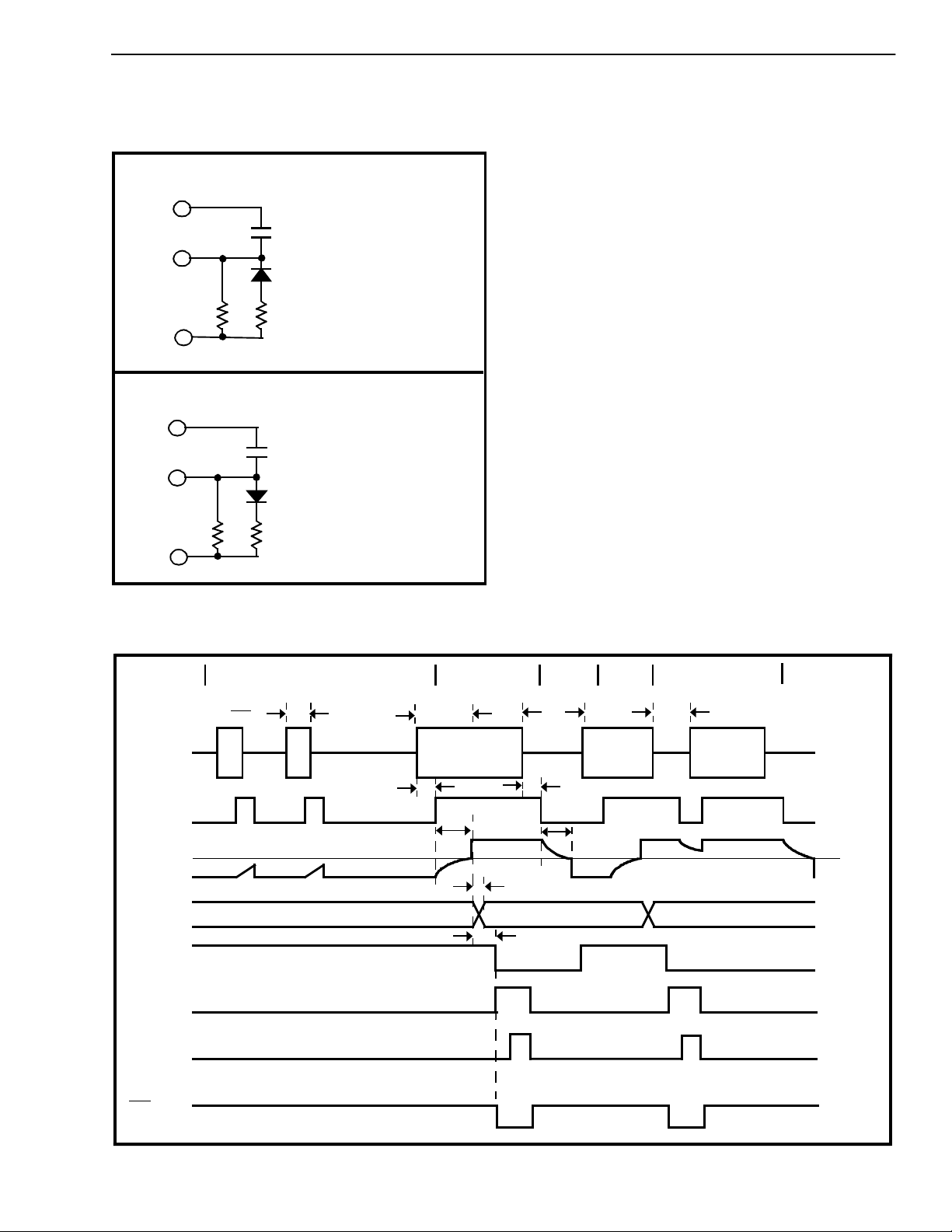
EVENTS
V
in
ESt
St/GT
RX
-RX
0
b3
b2
Read
Status
Register
/CP
IRQ
ABCDEF
t
t
REC
t
DP
3
DECODED TONE # (n-1)
REC
TONE #n
t
GTP
t
PStRX
t
PStb3
t
ID
# n
t
DO
TONE
#n + 1
t
DA
t
GTA
TONE
#n + 1
# (n + 1)
V
TSt
Figure 7 - R ece iver Tim ing Diag ram
4-55
Page 6
MT8885 Advance Information
AAAA
AAAA
A
A
A
A
AAAA
A
A
AA
EXPLANATION OF EVENTS
A) TONE BURSTS DETECTED, TONE DURATI ON INVALID, RX DATA REGISTER NOT UPDATED.
B) TONE #n DETECTED, TONE DURATION VALID, TONE DECODED AND LATCHED IN RX DATA REGISTER.
C) END OF TONE #n DETECTED, TONE ABSENT DURATION VALI D, INFORMATION IN RX DATA REGISTER
D) TONE #n+1 DETECTED, TONE DURATION VALID, TONE DECODED AND LATCHED IN RX DATA REGISTER.
E) ACCEPTABLE DROPOUT OF TONE #n+1, TONE ABSENT DURATION INVALID, DATA REMAINS UNCHANGED.
F) END OF TONE #n+1 DE TECTED, TONE A BSENT DURATION VALI D, I NFORMATION IN RX DATA REGISTER
EXPLANATION OF SYMBOLS
V
in
ESt EARLY S TEERING OUTPUT. INDICATES DETECTION OF VALID TONE FREQUENCIES.
St/GT STE ERING INPUT/GUARD TIME OUTPUT. DRIVES EXTERNAL RC TIMING CIRCUIT.
RX
0
b3 DELAYED STEERING. INDICATES THAT VALID FREQUENCIES HAVE BEEN PRESENT/ABSENT FOR THE
b2 INDICATES THAT VALI D DATA IS IN THE RE CEIVE DATA RE GISTER. THE BIT IS CLEARED AFTER THE STATUS
IRQ
t
REC
t
REC
t
ID
t
DO
t
DP
t
DA
t
GTP
t
GTA
RETAINE D UNTI L NEXT VALID TONE PAIR.
RETAINE D UNTI L NEXT VALID TONE PAIR.
DTMF COMPOSITE INPUT SIG NA L.
-RX34-BIT DECODED DATA IN RECEIVE DATA REGISTER
REQUIRED GUARD TIME THUS CONSTITUTING A VALID SIGNAL. ACTIVE LOW FOR THE DURATION OF A
VALID DTMF SIGNAL.
REGISTER IS READ.
/CP INTERRUPT IS ACTIVE INDICATING THAT NEW DATA IS IN THE RX DATA REGISTER. THE INTERRUPT IS
CLEARED AFTER THE STAT US R EGI STER IS READ.
MAXIMUM DTMF SIGNAL DURATION NOT DETECTED AS VALID.
MINIMUM DTMF SIGNAL DURATION REQUIRED FOR VALID RECOGNITION.
MINIMUM TIME BET WEEN VALID SEQUENTI AL D TMF SIG NAL S.
MAXIMUM ALLOWABLE DROPOUT DURING VALID DTMF SIGNAL.
TIME TO DETECT VALID FREQUENCIES PRESENT.
TIME TO DETECT VALID FREQUENCIES ABSENT.
GUARD TIME, TO NE PR ESEN T.
GUARD TIME, TO NE ABSEN T.
Figur e 9 - De scri pt ion of Tim in g Ev en ts
DTMF signals cannot be detected if CP mode has
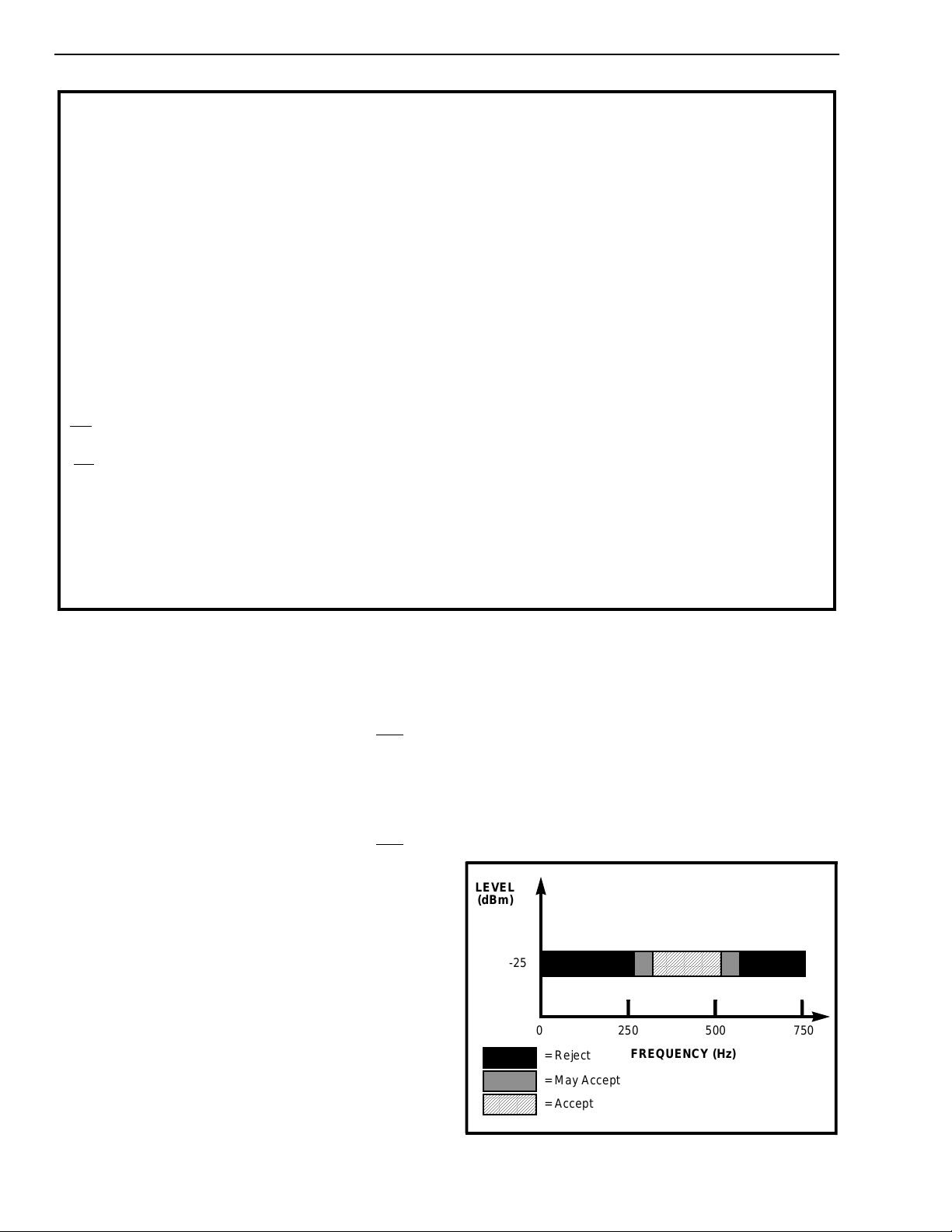
been selected (see Table 7). Figure 8 indicates the
useful detect bandwidth of the call progress filter.
Frequencies presented to the input, which are within
the ‘accep t’ bandwidth limits of the filter, are hardlimited by a high gain comparator with the IRQ/CP
pin serving as the output. The squarewave output
obtained from the schmitt trigger c an be analyzed by
a microprocessor or counter arrangement to
determine the nature of the call progress tone being
detected. Frequencies which are in the ‘reject’ area
will not be detected and consequently the IRQ
/CP
pin will remain low.
DTMF Generator
The DTMF transmitter employed in the MT8885 is
capable of generating all sixteen standard DTMF
tone pairs with low distortion and high accuracy. All
frequencies are derived from an external 3.579545
MHz crystal. The sinusoidal waveforms for the
individual tones are digitally synthesized using row
and column programmable dividers and switched
capacitor D/A converters. The row and column tones
are mixed and filtered providing a DTMF signal with
low total harmonic distortion and high accuracy. To
specify a DTMF signal, data conforming to the
encoding format s hown in Table 1 must be written to
the transmit Data Register. Note that this is the
same as the receiver output code. The individual
tones which are generated (f
LOW
and f
HIGH
) are
referred to as Low Group and High Group tones. As
seen from the table, the low group frequencies are
697, 770, 852 and 941 Hz. The high group
frequencies are 1209, 1336, 1477 and 1633 Hz.
Typically, the high group to low group amplitude ratio
(twist) is 2 dB to com-pensate for high group
attenuation on long loops.
LEVEL
(dBm)
AAA
AAAA
AAAA
AAA
AAAA
-25
AAA
AAAA
AAAA
AAAA
0250500750
= Reject
FREQUENCY (Hz)
= May Accept
AAA
AAAA
A
AAAA
= Accept
A
AAA
Figure 8 - Call Progress Response
4-56
Page 7

Advance Information MT8885
Scaling Information
10 dB/Div
Start Frequency = 0 Hz
Stop Frequency = 3400 Hz
Marker Frequency = 697 Hz and
1209 Hz
Figure 10 - Spectrum Plot
The period of each tone consists of 32 equal time
segments. The period of a tone is controlled by
varying the length of these time segments. During
write operations to the Transmit Dat a Regis ter the 4
bit dat a on the bus is latched and converted to 2 of 8
coding for use by the programmable divider circuitry.
This code is used to specify a time segment length,
which will ultimately determine the frequency of the
tone. When the divider reaches the appropriate
count, as determined by the input code, a reset pulse
is issued and the counter starts again. The number
of time segments is fixed at 32, however, by varying
the segment length as described above the
frequency can also be varied. The divider output
clocks another counter, which addresses the
sinewave lookup ROM.
The lookup table contains codes which are used by
the switched capacitor D/A converter to obtain
discrete and highly accurate DC voltage lev els. Two
identical circuits are employed to produce row and
column tones, which are then mixed using a low
noise summing amplifier. The oscillator described
needs no “start-up” time as in other DTMF
generators since the crystal oscillator is running
continuously thus providing a high degree of tone
burst accuracy. A bandwidth limiting filter is
incorporated and serves to attenuate distortion
products above 8 kHz. It can be seen from Figure 6
that the distortion products are very low in amplitude.
application or by any one of the exchange tr ansmitter
specifications currently existing. Standard DTMF
signal timing can be accomplished by m aking use of
the Burst M o de. T h e tra n smitter is ca p abl e of is sui n g
symmetric burst s/pauses of predeterm ined duration.
This burst/pause duration is 51 ms±1 ms which is a
standard interval for autodialer and central office
applications. After the burst/pause has been issued,
the appropriate bit is set in the Status Register
indicating that the transmi tter is re a d y fo r more d at a.
The timing described above is available when DTMF
mode has been selected. However, when CP mode
(Call Progress mode) is selected, the burst/pause
duration is d ou b le d to 1 02 ms ±2 ms. Note th a t wh e n
CP mode and Burst mode have been selected,
DTMF tones may be transmitted only and
not
received. In applications where a non-standard
burst/pause time is desirable, a software timing loop
or external t imer can be used to provide the timing
pulses when the burst mode is disabled by enabling
and disabling the transmitter.
Single Tone G eneration
A single tone mode is available whereby individual
tones from the low group or high group can be
generated. This mode can be used for DTMF test
equipment applications, acknowledgment tone
generation and distortion measurements. Refer to
Control Register B description for details.
Burst Mode
In certain telephony applications it is required that
DTMF signals being generated are of a specific
duration determined either by the particular
4-57
Page 8

MT8885 Advance Information
ACTIVE
INPUT
L1
L2
L3
L4
H1
H2
H3
H4
OUTPUT FREQUENCY (Hz)
SPECIFIED ACTUAL
697 699.1 +0.30
770 766.2 -0.49
852 847.4 -0.54
941 948.0 +0.74
1209 1215.9 +0.57
1336 1331.7 -0.32
1477 1471.9 -0.35
1633 1645.0 +0.73
%ERROR
Table 2. Actual Frequencies Versus Standard
Requirements
Distortion Calculations
The MT8885 is capable of producing precise tone
bursts wit h minimal error in frequency (see Table 2).
The internal summing amplifier is followed by a firstorder lowpass switched capacitor filter to minimize
harmonic components and intermodulation products.
The total harmonic distort ion for a
calculated using Equation 1, which is the ratio of the
total power of all the extraneous frequencies to the
power of the fundamental fr equency expressed as a
percentage.
single tone
can be
DTMF Clock Circuit
The internal clock circuit is completed with the
addition of a standard telev ision colour burst crystal
having a resonant frequency of 3.579545 MHz. A
number of MT8885 devices can be connected as
shown in Figure 11 such that only one crystal is
required. Alternatively, the OSC1 inputs on all
devices can be driven from a TTL buffer with the
OSC2 outputs left unconnected.
MT8885
OSC1 OSC2
3.579545 MHz
MT8885
OSC1 OSC2
MT8885
OSC1 OSC2
Figure 11 - Common Crystal Connection
Microprocessor Interfa ce
The MT8885 design incorporates an adaptive
interface, which allows it to be connected to various
kinds of microprocessors. Key functions of this
interface include the following:
2
2
THD (%) = 100
V
+ V
2f
V
+ V
3f
fundamental
2
4f
+ .... V
2
nf
Equation 1 . THD (%) For a Single Tone
The Fourier components of the tone output
correspond to V
waveform. The total harmonic distortion for a
tone
can be calculated using Equation 2. V
correspond to the low group amplitude and high
group amplitude, respectively and V
.... Vnf as measured on t he output
2f
and V
L
2
is the sum
IMD
dual
of all the intermodulation components. The internal
switched-capacitor filter following the D/A converter
keeps distort ion products down to a very low level as
shown in Figure 10.
2
THD (%) = 100
2L
+ V
V
2
3H
2
3L
+ .. V
V
V
+ .... V
2
+ V
L
2
2
+ V
2
IMD
2H
+
nL
2
+ V
nH
2
H
Equation 2. THD (% ) For a Dual Tone
• Continuous activity on DS/RD
is not necessary
to update the internal status registers.
• senses whe t her in pu t t imi ng is tha t of an I nte l o r
Motorola controller by monitoring the DS (RD
(WR) an d CS inputs.
R/W
• gene rates equiva lent CS
signal for internal
operatio n for all proc ess ors.
H
• different iates betw een m ultip lexed a nd n onmultiplexed microprocessor buse s. Address
and data ar e lat ched in accord ingly.
• compatible with Motorola and Intel processors.
Figure 16 shows the timing diagram for Motorola
microprocessors with separate address and data
buses. Members of this microprocessor family
include 2 MHz versions of the MC6800, MC6802 and
MC6809. For the MC6809, the chip select (CS
signal is formed by NANDing the (E+Q) clocks and
address decode output. For the MC6800 and
MC6802, CS
is formed by NANDing VMA and
address decode output. On the falling edge of CS
the internal logic senses the state of data strobe
),
) inpu t
,
4-58
Page 9

Advance Information MT8885
(DS). When DS is low, Motorola processor operation
is selected.
Figure 17 shows the tim ing diagram for the Motorola
MC68HC11 (1 MHz) microcontroller. The chip select
) input is formed by NANDing address strobe
(CS
(AS
) and address decode output. Again, the MT8885
examines the state of DS on the falling edge of CS
to
determine if the micro has a Motorola bus (when DS
is low). Additionally, the Texas Instruments
TMS370CX5X is qualified to have a Motorola
interface. Figure 12(a) summarizes connection of
these Motorola processors to the MT8885 DTMF
transceiver.
Figures 18 and 19 are the timing diagrams for the
Intel 8031/8051 (12 MHz) and 8085 (5 MHz) microcontrollers with multiplexed address and data buses.
The MT8885 latches in the state of RD
edge of CS
. When RD is high, Intel processor
on the falling
operation is selected. By NANDing the address
latch enable (ALE) output with the high-byte address
(P2) decode output, CS
can be generated. Figure
12(b) summarizes the connection of these Intel
processors to the MT8885 transceiver.
NOTE: The adaptive micro interface relies on highto-low transition on CS
microcontroller interface and this pin must not
to recognize the
be tied
permanently low.
The adaptive micro interf ace provides access to five
internal registers. The read-only Receive Data
Register contains the decoded output of the last
valid DTMF digit received. Data entered into the
write-only Transmit Data Register will determine
which tone pair is to be generated (see Table 1 for
coding details). Transceiver control is accomplished
with two control registers (see Tables 6 and 7), CRA
and CRB, which have the same address. A write
operation to CRB is executed by first setting the
most significant bit (b3) in CRA. The following write
operation to the same address will then be directed
to CRB, and subsequent write c ycles w ill b e dir ected
back to CRA. The read-only status register indicates
the current transceiver state (see Table 8).
A software reset must be included at the beginning
of all programs to initialize the control registers upon
power-up or power reset (see Figure 14). Refer to
Tables 4-7 for bit descriptions of the two control
registers.
The multiplexed IRQ
/CP pin can be programmed to
generate an interrupt upon validation of DTMF
signals or when the transmitter is ready for more
data (burst m ode only). Alternatively, this pin can be
configured to provide a square-wave output of the
call progress signal. The IRQ
/CP pin is an open drain
output and requires an external pull-up resistor (see
Figure 13).
MC6800/6802
A0-A15
VMA
D0-D3
RW
Φ2
MC6809
A0-A15
Q
E
D0-D3
R/W
Figure 12 a) & b) - MT8885 Interface Connections for Various Intel and Motorola Micros
(a)
MT8885
CS
RS0
D0-D3
R/W
/WR
DS/RD
MT8885
CS
RS0
D0-D3
R/W/WR
DS/RD
MC68HC11
A8-A15
AS
AD0-AD3
DS
RW
8031/8051
8080/8085
A8-A15
ALE
P0
RD
WR
(b)
MT8885
CS
D0-D3
RS0
DS/RD
R/W
/WR
MT8885
CS
D0-D3
RS0
DS/RD
R/W/WR
4-59
Page 10

MT8885 Advance Information
Motorola Intel
RS0 R/W
0001
0110
1001
1110
WR RD FUNCTION
Write to Transmit
Data Registe r
Read from Receive
Data Registe r
Write to Control Register
Read from Status Register
Table 3. Internal Regis ter Fu nctio ns
b3 b2 b1 b0
RSEL IRQ CP/DTMF
Ta ble 4. CRA B it Positions
b3 b2 b1 b0
C/R
S/D TE ST BURST
Ta ble 5. CRB B it Positions
TOUT
ENABLE
BIT NAME DESCRIPTION
b0 TOUT Tone Output Control. A logic high enables the tone output; a logic low turns the tone output
off and places the complete DTMF transmitter circuit in power down mode. This bit
controls all transmit tone functions.
b1 CP/DTMF
Call Progress or DTMF Mode Sele ct. A logic high enables the receive call progress mode;
a logic low enables DTMF mode. In DTMF mode the device is capable of receiving and
transmitting DTMF signals. In CP m ode a retangular wave rep r esentation of the re ceived
tone signal will be present on the IRQ
/CP output pin if IRQ has been enabled (control
register A, b2=1). In order to be detected, CP signals must be within the bandwidth
specified in the AC Electrical Characteristi cs for Call Progress.
Note: DTMF signals cannot be detected when CP mode is selected .
b2 IRQ Interrupt Enable. A logic high enables the interrupt function; a logic low de-activate s the
interrupt function. When IRQ is en abled and DTM F mode is selected (cont rol registe r A,
b1=0), the IRQ
/CP output pin will go low when either 1) a va lid DTMF signal has been
received for a valid guard time duration, or 2) the transm itter is ready for more data (burst
mode only).
b3 RSEL Register Select. A logic high selects control register B for the next write cycle to the
control register address. Afte r w riting to control register B, the following cont rol register
write cycle will be directed to control register A.
Table 6. Control Register A Description
4-60
Page 11

Advance Information MT8885
BIT NAME DESCRIPTION
b0 BURST
b1 RxEN
b2 S/D
b3 C/R
Burst Mode Sel ect. A logic hig h de-act ivat es burst mod e; a logi c low e nables b ur st mode.
When activated, t he digital code representing a DTMF sig nal (see Table 1) can be written
to the transmit register, which will re sult in a transmit DTMF tone burst and pause of e qual
durations (typically 51 msec). Following the pause, the status register will be updated (b1 Transmit Data Register Empty), and an inte rrupt will occur if the interrupt mode has been
enabled.
When CP mode (control register A, b1) is enabled the normal tone burst and pause
durations are extended from a typical duratio n of 51 msec to 102 msec.
When BURST is high (de-activated) the transmit tone burst duration is determined by the
TOUT bit (control register A, b0).
This bit enables the DTMF and Call Progress Tone receivers. A logic low enables both
circuits. A logic high deactivates and puts both receiver circuits int o power down mod e.
Single or Dual Tone Generat ion. A logic high selects the single tone output ; a logic low
selects the dual tone (DTM F) outpu t. The single tone generat ion function requ ires furthe r
selection of either t he row or colum n tones (l ow or hi gh group ) throu gh the C /R
register B, b3).
Column or Row Tone Select. A logic high selects a column tone output; a logic low selects
a row tone outp ut. Th is f unction is used in conjunctio n wi th th e S/D
b2).
Ta ble 7. Contr ol Register B Des cription
bit (control regi ster B,
bit (control
BIT NAME STATUS FLAG SE T STATUS FLAG CLEARE D
b0 IRQ Interrupt has occurred. Bit one
(b1) or bit two (b2) is set.
b1 TRANSM I T DATA
REGISTER EMPTY
(BURST MODE ONLY)
b2 RECEIVE DATA REGISTER
FULL
b3 DELAYED
STEERING Set upon the valid detection of
Pause duration has terminat ed
and transmitter is ready for new
data.
Valid data is in t he Receive Dat a
Register.
the absence of a DTMF signal.
Table 8
. Status Register Description
Interrupt is inactive. Cleared after
Status Register is read.
Cleared after Status Register is
read or when in non-burst mode.
Cleared after Status Register is
read.
Cleared upon the detection of a
valid DTMF signal.
4-61
Page 12

MT8885 Advance Information
V
DD
DTMF/CP
INPUT
DTMF
OUTPUT
C1
R1
R2
X-tal
R
MT8885
IN+
INGS
VRef
VSS
OSC1
OSC2
NC
NC
TONE
R/W
L
/WR
CS
VDD
St/GT
ESt
PWDN
IRQ
/CP
DS/RD
RS0
D3
D2
D1
D0
NC
C2
R3
C3
R4
To µP
or µC
Notes:
R1, R2 = 100 kΩ 1%
R3 = 374 Ω 1%
R4 = 3.3 kΩ 10%
RL = 10 k Ω (min.)
C1 = 100 nF 5%
C2 = 100 nF 5%
C3 = 100 nF 10%*
X-tal = 3.579545 MHz
* Microprocessor based systems can inject undesirable noise into the supply rails.
The performance of the MT8885 can be optimized by keeping
noise on the supply rails to a minimum. The decoupling capacitor (C3) should be
connected close to the de vice and g round loo ps sho uld be avoided.
Figure 1 3 - Application Circuit (Single-Ended Input)
4-62
Page 13

Advance Information MT8885
INITIALI ZATION PROCEDURE
A software reset must be included at the beginning of all programs to initialize the control registers after
pow er up .
Description: Motorola
RS0 R/W
Intel Data
WR RD b3 b2 b1 b0
1) Read Status Register 1 1 1 0 X X X X
2) Write to Control Register 1 0 0 1 0 0 0 0
3) Write to Control Register 1 0 0 1 0 0 0 0
4) Write to Control Register 1 0 0 1 1 0 0 0
5) Write to Control Register 1 0 0 1 0 0 0 0
6) Read Status Register 1 1 1 0 X X X X
TYPICAL CONTROL SEQ UE NCE FOR BURS T MO DE APP LIC ATIONS
Transmit DTMF tones of 50 ms burst/50 ms pause and Receive DTMF Tones.
Sequence:
RS0 R/W
WR RD b3 b2 b1 b0
1) Write to Control Register A 1 0 0 1 1 1 0 1
(tone out, DTMF, IRQ
, Select Con tr ol Register B)
2) Write to Control Register B 1 0 0 1 0 0 0 0
(burst mode)
3) Write to Transmit Data Reg ister 0 0 0 1 0 1 1 1
(send a digit 7)
4) Wait for an Interr upt or Poll S ta tu s R e gis te r
5) Read the Status Register 1 1 1 0 X X X X
-if bit 1 is s e t, th e T x is ready for the ne x t to n e, in which case .. .
Write to Transm it Register 0 0 0 1 0 1 0 1
(send a digit 5)
-if bit 2 is set, a DTMF tone has been receiv ed, in which case ....
Read the Receive Data Register 0 1 1 0 X X X X
-if both bits a re set ...
Read the Receive Data Register 0 1 1 0 X X X X
Write to Transm it Data Reg ister 0 0 0 1 0 1 0 1
NOTE: IN THE TX BURST MODE, STATUS REGISTER BIT 1 WILL NOT BE SET UNTIL 100 ms ( ±2 ms) AFTER THE DATA IS
WRITTEN TO THE TX DATA REGISTER. IN EXTENDED BURST MODE THIS TIME WILL BE DOUBLED TO 200 ms (± 4 ms)
Figure 14 - Application Notes
4-63
Page 14

MT8885 Advance Information
Absolute Maximum Ratings*
Parameter Symbol Min Max Units
1 Power supply voltage V
DD-VSS
2 Voltage on any pin V
3 Current at any pin (Except V
DD
and VSS
)10mA
4 Storage temperature T
5 Package power dissipation P
* Exceeding these values may cause perm anen t damage . Functi onal operati on under the se cond itions is not impl ied.
Recommended Operating Conditions - Voltages are with respect to ground (V
Parameter Sym Min Typ
1 Positive power supp ly V
2 Operating temperature T
3 Crystal clock frequency f
‡ Typical figures are at 25 °C and for design aid only: not guarante ed and not subject to producti on test ing.
DC Electrical Characteristics
DD
O
CLK
†
- VSS=0 V.
4.75 5.00 5.25 V
-40 +85 °C
3.575965 3.579545 3.583124 MHz
V
DD
I
ST
D
‡
Max Un its Test Conditions
VSS-0.3 VDD+0.3 V
-65 +150 °C
) unless otherwise stated.
SS
Characteristics Sym Min Typ‡Max Units Test Conditions
1
2 O perating supply current I
3 Standby supply current 25 µA PWDN= V
4
5 Low level input voltage
6 Steering threshold voltage V
7
8 H igh level out put volta ge
9 O utput lea kage current
10 V
11 V
12
13 High level input voltage V
14 Input leakage current I
15
16 Sink current I
17
18 Sink current I
19
† Characteristics are over recommended operating conditions unless otherwise stated.
‡ Typical figures are at 25 °C, V
* See “Notes” following AC Electrical Chara ct erist ic s Tab le s.
Operating supply volta ge V
S
U
P
High level input voltage
I
(OSC1)
N
P
U
(OSC1)
T
S
Low level output volt age
(OSC2) V
O
U
T
(OSC2) V
P
U
(IRQ) I
T
S
D
i
g
i
t
a
l
Data
Bus
ESt
and
St/GT
IRQ/
CP
output voltage V
Ref
output resi sta n ce R
Ref
Low level input voltage V
Source current I
Source current I
Sink current I
=5V and for design aid only: not guaranteed and not subje ct to produ ctio n testi ng.
DD
V
V
DD
DD
IHO
ILO
TSt
OLO
OHO
OZ
Ref
OR
IL
IH
IZ
OH
OL
OH
OL
OL
4.75 5.0 5.25 V
7.0 11 mA
3.5 V Note 9*
1.5 V Note 9*
2.2 2.3 2.5 V VDD=5V
No load
0.1 V
Note 9*
No load
4.9 V
Note 9*
110µAVOH=2.4 V
2.4 2.5 2.6 V No load, VDD=5V
1.3 kΩ
0.8 V
2.0 V
10 µAVIN=V
-1.4 -6.6 mA VOH=2.4V
2.0 4.0 mA VOL=0.4V
-0.5 -3.0 mA VOH=4.6V
24 mAV
OL
=0.4V
416 mAVOL=0.4V
6V
1000 mW
DD
to V
SS
DD
4-64
Page 15

Advance Information MT8885
Electrical Characteristics
Gain Setting Amplifier - Voltages are with respect to ground (V
Characteristics Sym Min Typ
) unless otherwise stated, VSS= 0V, VDD=5V, TO=25°C.
SS
‡
Max Un its Test Con ditio ns
1 Input leakage current I
2 Input resistance R
3 Input offset voltage V
IN
IN
OS
±100 nA VSS ≤ V
10 M Ω
25 mV
4 Power supply reject ion PSRR 60 dB 1 kHz
5 Co mm on mo de rejecti on CMRR 60 dB 0.75 ≤ V
6 DC open loop voltage gain A
VOL
65 dB
7 Un ity gain b an dwidt h BW 1.5 MHz
8 O utp ut voltage swing V
9 Allowable capacitive load (GS) C
10 Allowable resistive load (GS) R
11 Common mo de ra nge V
‡ Typical figures are at 25°C and for design ai d only: not guarantee d and not subject to productio n testi ng.
MT8885 AC Electrical Characteristics
O
L
L
CM
†
- Volt ages are with respect to ground (V
4.5 V
100 pF
50 kΩ
3.0 V
pp
pp
SS
RL ≥ 100 kΩ to V
) unless otherwise stated.
No Load
Characteristics Sym Min Typ‡Max Units Notes*
Valid input signal levels
R
1
† Characteristics are over recommended operating conditions (unless otherwise stated)
(each tone of composite
X
signal)
-29 +1 dBm 1,2,3,5,6
27.5 869 mV
using the test circuit shown in Figure 13.
RMS
1,2,3,5,6
≤ V
IN
≤ 4.25V
IN
DD
SS
AC Electrical Characteristics† - Voltages are with respect to ground (V
) unless otherwise stated. fC=3.579545 MHz
SS
Characteristics Sym Min Typ‡Max Units Notes*
1
Positive twist accept 8 dB 2,3,6,9
2 Negative twist accept 8 dB 2,3,6,9
3 Freq. deviation accept ±1.5%± 2Hz 2,3,5
R
4 Freq. deviation reject ±3.5% 2,3,5
X
5 Third tone tolerance -16 dB 2,3,4,5,9 ,10
6 Noise tolerance -12 dB 2,3,4,5,7,9,10
7 Dial tone toleran ce 22 dB 2,3,4,5,8,9
† Characteristics are over recommended operating conditions unless otherwise stated.
‡ Typical figures are at 25°C, V
* *See “Notes” following AC Elect rical Charact erist ic s Tab le s.
= 5V, and for design aid only: not guaranteed and not subject to produ ctio n testing .
DD
4-65
Page 16

MT8885 Advance Information
AC Electrical Characteristics†- Call Progress - Voltages are with respect to ground (V
), unless otherwise stated .
SS
Characteristi cs Sym Min Typ‡Max Units Cond iti ons
1 Accept Bandwidth f
A
310 500 Hz @ -25 dBm,
Note 9
2 Lower freq. (REJECT) f
3 Upper freq. (REJECT) f
4 Call progress tone detect level (total
LR
HR
-30 dBm
290 Hz @ -25 dBm
540 Hz @ -25 dBm
power)
† Characteristics are over recommended operating conditions unless otherwise stated
‡ Typical figures are at 25°C, V
=5V, and for design aid only: not guaranteed and not subject to production testing
DD
AC Electrical Characteristics†- DTMF Reception - Typical DTMF tone accept and reject req uirem ents. Actual
values are user selectable as per Figures 5, 6 and 7.
Characteristics Sym Min Typ
1 Minimum tone accept duration t
2 Maximum tone reject duration t
3 Minimum int erdigit pause duration t
4 Maximum tone drop-out duration t
† Characteristics are over recommended operating conditions unless otherwise stated
‡ Typical figures are at 25°C, V
=5V, and for design aid only: not guaranteed and not subject to production testing
DD
REC
REC
ID
OD
‡
Max Units Conditions
40 ms
20 ms
40 ms
20 ms
AC Electrical Characteristics† - Voltages are with respect to ground (V
Characteristics Sym Min Typ
T
1
2 Tone absent detect time t
3 Delay St to b3 t
4 Delay St to RX
5
6 Tone pause duration t
7 Tone burst duration (extended) t
8 Tone pau se duration (extended) t
9 High group output level V
10 Low group output level V
11 Pre-emphasis dBP 0 2 3 dB R
12 Output distortion (Single Tone) THD -35 dB 25 kHz Bandwidth
13 R
14 Frequency deviation f
15 Output load resistan ce R
16
17 Clock input rise and fall time t
18 Clock input duty cycle DC
19 Capacitive load (OSC2) C
† Timing is over recommended temperature & power supply voltages.
‡ Typical figures are at 25°C and for design aid only: not guaranteed and not subject to production testing.
Tone present detect time t
O
N
E
I
N
0
-RX
3
Tone burst duration t
T
O
N
E
O
U
T
Crystal/clock frequency f
X
T
A
L
DP
DA
PStb3
t
PStRX
BST
PS
BSTE
PSE
HOUT
LOUT
CLRF
3 11 14 ms Note 11
0.5 4 8.5 ms Note 11
50 52 ms DTMF mode
50 52 ms DTMF mode
100 104 ms Call Progress mode
100 104 ms Call Progress mode
-6.1 -2.1 dBm RL=10kΩ
-8.1 -4.1 dB m RL=10kΩ
D
LT
C
CL
LO
10 50 k Ω
3.5759 3.5795 3.5831 M Hz
40 50 60 % Ext. clo ck
), unless otherwise stated.
SS
‡
Max Units Conditions
13 µs See Figure 7
8 µs See Figure 7
=10kΩ
L
=10kΩ
L
±0.7 ±1.5 % fC=3.579545 MHz
110 ns Ext. cl o ck
30 pF
4-66
Page 17

Advance Information MT8885
AC Electrical Characteristics†- MPU Interface - Voltages are with respect to groun d (V
Characteristi cs Sym Min Typ
1DS/RD
2DS/RD
3DS/RD
4DS/RD
5DS/RD
6R/W
7R/W
8 Address setup time (RS0) t
9 Address hold time (RS0) t
10 Data hold time (read) t
11 DS/RD
12 Data setup time (write) t
13 Data hold time (write) t
14 Chip select setup time t
15 Chip select hold time t
16 Input Capacitance (data bus) C
17 Output Capacitance (IRQ
† Characteristics are over recommended operating conditions unless otherwise stated
‡ Typical figures are at 25°C, V
/WR clock frequency f
/WR cycle period t
/WR low pulse width t
/WR high pulse width t
/WR rise and fall time tR,t
setup time t
hold time t
to valid data delay (read) t
/CP) C
=5V, and for design aid only: not guaranteed and not subject to production testing
DD
CYC
CYC
CL
CH
RWS
RWH
AS
AH
DHR
DDR
DSW
DHW
CSS
CSH
IN
OUT
150 ns Figure 15
F
23 ns Figures 16 & 17
20 ns Figures 16 & 17
0 ns Figures 16 - 19
40 20 ns Figures 16 - 19
22 ns Figures 16 - 19
45 ns Figures 16 - 19
10 ns Figures 16 - 19
45 35 ns Figures 16 - 19
40 ns Figures 16 - 19
‡
Max Units Con di tions
4.0 MHz Figure 15
250 ns Figure 15
100 ns Figure 15
20 ns Figure 15
100 ns Figures 1 6 - 19
5pF
5pF
), unless otherwise stated.
SS
NOTES: 1) dBm=decibels above or below a reference power of 1 mW into a 600 ohm load.
2) Digit seq uence co ns is ts o f a ll 16 DTM F tones.
3) Tone duration=40 ms. Tone pause=40 ms.
4) Nominal DTMF frequencies are used.
5) Both tones in the composite signal have an equal amplitude.
6) The tone pa ir is dev iat ed by ± 1 .5 %±2 Hz.
7) Bandwid th limited (3 k H z) G au s si an noise.
8) The precise dial tone frequencies are 350 and 440 Hz (±2 %).
9) Guaranteed by design and characterization. Not subject to production testing.
10) Referenced to the low es t a mp li tu de to ne in the D TM F si gn al .
11 ) For guard t im e c a lc ul ation pur p os es .
t
CYC
DS/RD/WR
t
R
t
CH
t
F
t
CL
Figure 15 - D S /RD/WR Clock Pulse
4-67
Page 18

MT8885 Advance Information
DS
Q clk*
A0-A15
(RS0)
R/W(read)
Read Data
(D3-D0)
(write)
R/W
Write data
(D3-D0)
CS
= (E + Q).Addr [MC6809]
= VMA.Addr [MC6800, MC6802]
CS
*microprocessor pin
t
RWS
t
RWH
16 bytes of Addr
t
DDR
➀
t
DSW
t
CSS
t
AH
t
AS
t
AS
t
CSS
➀
t
CSH
t
AH
➀
t
CSH
t
DHR
t
DHW
➀ t
is fro m da ta to DS fal li ng ed ge ; t
DSW
DS
R/W
Read
AD3-AD0
(RS0, D0-D3)
Write
AD3-AD0
(RS0-D0-D3)
Addr *
non-mux
AS *
Figure 16 - MC6800/MC6802/MC6809 Timing Diagram
is from D S ris in g ed ge to CS risin g edge .
CSH
t
RWS
t
t
AS
Addr
Addr
t
AH
High Byte of Addr
DDR
t
CSH
t
DSW
t
DHR
Data
Data
t
DHW
t
RWH
CS = AS.Addr
* microprocessor pins
4-68
t
CSS
Figure 17 - M C68H C11 Bus Timing (w ith multip lexed addr ess an d data bus es)
Page 19

Advance Information MT8885
t
CSS
ALE*
RD
t
DHR
P0*
(RS0,
D0-D3)
t
AS
A0-A7
t
AH
t
DDR
Data
P2 *
(Addr)
= ALE.Addr
CS
* microprocessor pins
ALE*
WR
P0*
(RS0,
D0-D3)
P2 *
(Addr)
A8-A15 Address
t
CSH
Figure 18 - 8 031 /8051/ 8085 Rea d Timing Dia gram
t
CSS
t
t
AS
A0-A7
t
AH
DSW
t
Data
A8-A15 Address
DHW
= ALE.Addr
CS
* microprocessor pins
t
CSH
Figure 19 - 80 31/8 05 1/8085 Wri te Timin g D iagra m
4-69
Page 20

MT8885 Advance Information
NOTES:
4-70
 Loading...