

Page 1

E2D0083-27-44
Preliminary
¡ Semiconductor MSM9888L
¡ Semiconductor
This version: Jan. 1998
Previous version: May. 1997
MSM9888L
Flash-driving Recording and Playback IC
GENERAL DESCRIPTION
The MSM 9888L is a recording and playback IC that is controlled by the micro-controller in serial
mode, compresses voice with the Oki ADPCM system with high tone quality, and directly stores
voice data inthe serial voice flash momory. This IC can operate in a range of 2.7 to 3.6 V and
contains a mask ROM. Since the package is small and backup is not needed, this recording and
playback IC is suitable for the voice system such as handy terminals.
FEATURES
• Voice analyzing and synthesizing system
: 4-bit OKI ADPCM system•8-bit OKI non-linear PCM system
(for ROM playback only)
• Built-in 12-bit A/D•D/A converter
• Built-in LPF : Attenuation rate –40 dB/oct
• Sampling frequency (for 4.096 MHz of source oscillation frequency)
: 2.0 kHz, 2.7 kHz, 3.2kHz, 4.0 kHz, 5.3 kHz, 6.4 kHz, 8 kHz
• External memory for variable message
: 1Mb, 2Mb, 4Mb, 8Mb, serial voice flash memory
• Recording time (When the 1Mb serial voice flash is used)
: Approximately 32 seconds (Fsam=8.0 kHz)
: Approximately 40 seconds (Fsam=6.4 kHz)
: Approximately 65 seconds (Fsam=4.0 kHz)
• Built-in 512Kb mask ROM for fixed message
• Playback time for fixed message
: Approximately 15 seconds (Fsam=8.0 kHz)
: Approximately 20 seconds (Fsam=6.4 kHz)
: Approximately 31 seconds (Fsam=4.0 kHz)
• Number of pharase
Variable message : 63 phrases
Fixed message : 255 phrases
• Any data can be written to and read from a part in the voice flash memory.
• Serial microcontroller interface
• Source oscillation frequency : 4 MHz to 6 MHz
• Supply voltage : 2.7 V to 3.6 V
• Operating temperature : –10°C to 70°C
• Package :
30-pin plastic SSOP (SSOP30-P-56-0.65-K)(Product name : MSM9888LGS-AK)
1/14
Page 2
¡ Semiconductor MSM9888L
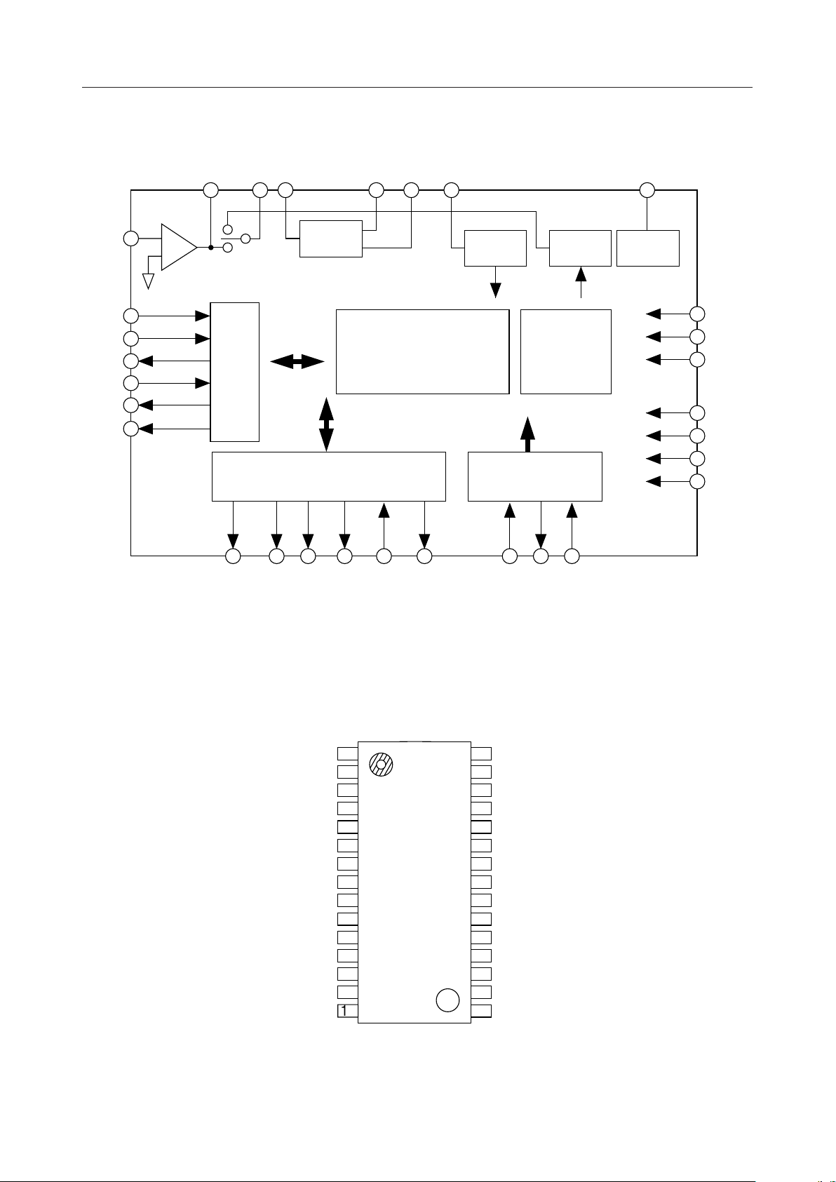
BLOCK DIAGRAM
ADINAOUTFOUTFINLOUT AMON SG
LIN
CS
DI
DO
SCK
BUSY
MON
MCU
I/F
LPF
ADPCM/PCM
Analyzer/Synthesizer
Flash Controller Timing Controller
ADC DAC SG
ROM
512Kbit
MASK ROM
RESETXTXTFDIFDOFSCKFCSFPRTFRESET
TEST0
TEST1
TEST2
AV
DD
AGND
DV
DD
DGND
PIN CONFIGURATION (TOP VIEW)
SG
1
AMON
FOUT
AOUT
DV
2
FIN
3
ADIN
4
5
6
AV
7
DD
8
DD
9
CS
XT
10
XT
11
SCK
12
DO
13
DI
14
15 16MON RESET
30-Pin Plastic SSOP
30
29
28
27
26
25
24
23
22
21
20
19
18
17
AGND
LOUT
LIN
FRESET
FPRT
FCS
FSCK
FDI
FDO
DGND
BUSY
TEST2
TEST1
TEST0
2/14
Page 3
¡ Semiconductor MSM9888L
PIN DESCRIPTION
Pin
14
17-19
Symbol I/O Description
Inputs the 8-bit command data.DI I
Outputs the 8-bit status data.DO O13
Inputs the data transfer clock for the DI and DO pins.SCK I12
CS I9
BUSY O20
XT I10
XT O11
RESET I16
LIN I28
LOUT O29
ADIN I4
AMON O2
FIN I3
FOUT O5
AOUT O6
TEST0-2 I LSI testing pins. Fix to "L".
DV
AV
DD
DD
—8
—7
Accepts the SCK pulse, when CS is "L" level. Does not accept the SCL pulse
when CS is "H" level.
Indicates "H" level during command execution. When driven high, do not input a
command from the external micro-controller.
Outputs "H" level during recording or playback.MON O15
1s connected to the DI pin of the serial voice flash memory.FDI O23
1s connected to the DO pin of the serial voice flash memory.FDO I22
1s connected to the SCK pin of the serial voice flash memory.FSCK O24
1s connected to the CS pin of the serial voice flash memory.FCS O25
1s connected to the PRT pin of the serial voice flash memory.FPRT O26
1s connected to the RESET pin of the serial voice flash memory.FRESET O27
Oscillator connecting pins. When using an external clock, input the clock from
the XT pin and keep the XT pin open.
The LSI is reset and starts oscillation when "L" level is input, keep "L" level during
oscillation stabilization time. Set to "H" level after oscillation stabilizes.
Analog reference voltage (Signal Ground) output pinSG O1
Built-in OP amplifier's invention input pin. The non-invention input pin is
internally connected to SG.
Built-in OP amplifier's output pin
Built-in 12-bit AD converter's input signal
Connected to the LOUT pin when recording mode, and to the DA converter's
output pin when playback mode. Connected to the built-in LPF's input (FIN pin).
Built-in LPF's input pin
Built-in LPF's output pin. Connected to the AD converter's input (ADIN pin).
Built-in LPF's output pin. This is the output pin the played back waveform and
connected to the speaker driving amplifier.
Digital power supply pin. Insert a bypass capacitor of 0.1mF or higher between
this pin and DGND pin.
Digital DGND pinDGND —21
Analog power supply pin. Insert a bypass capacitor of 0.1mF or higher between
this pin and AGND pin.
Analog GND pinAGND —30
3/14
Page 4
¡ Semiconductor MSM9888L
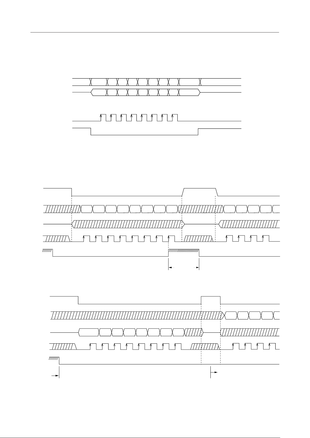
TIMING DIAGRAM
Flash driving Timing
MSB LSB
FDI
FDO
FSCK
FCS
MCU I/F driving Timing
<When data write>
CS
DI
DO
SCK
BUSY
Hi-Z
<When data read>
CS
DI
DO
First byte Second byte
MSB 2 3 4 5 6 7 LSB MSB 2 3 4
Data I/O not
permitted
MSB 2 3 4
MSB 2 3 4 5 6 7 LSB
SCK
BUSY
Preparation for
output data
Next data can
be input
4/14
Page 5
¡ Semiconductor MSM9888L
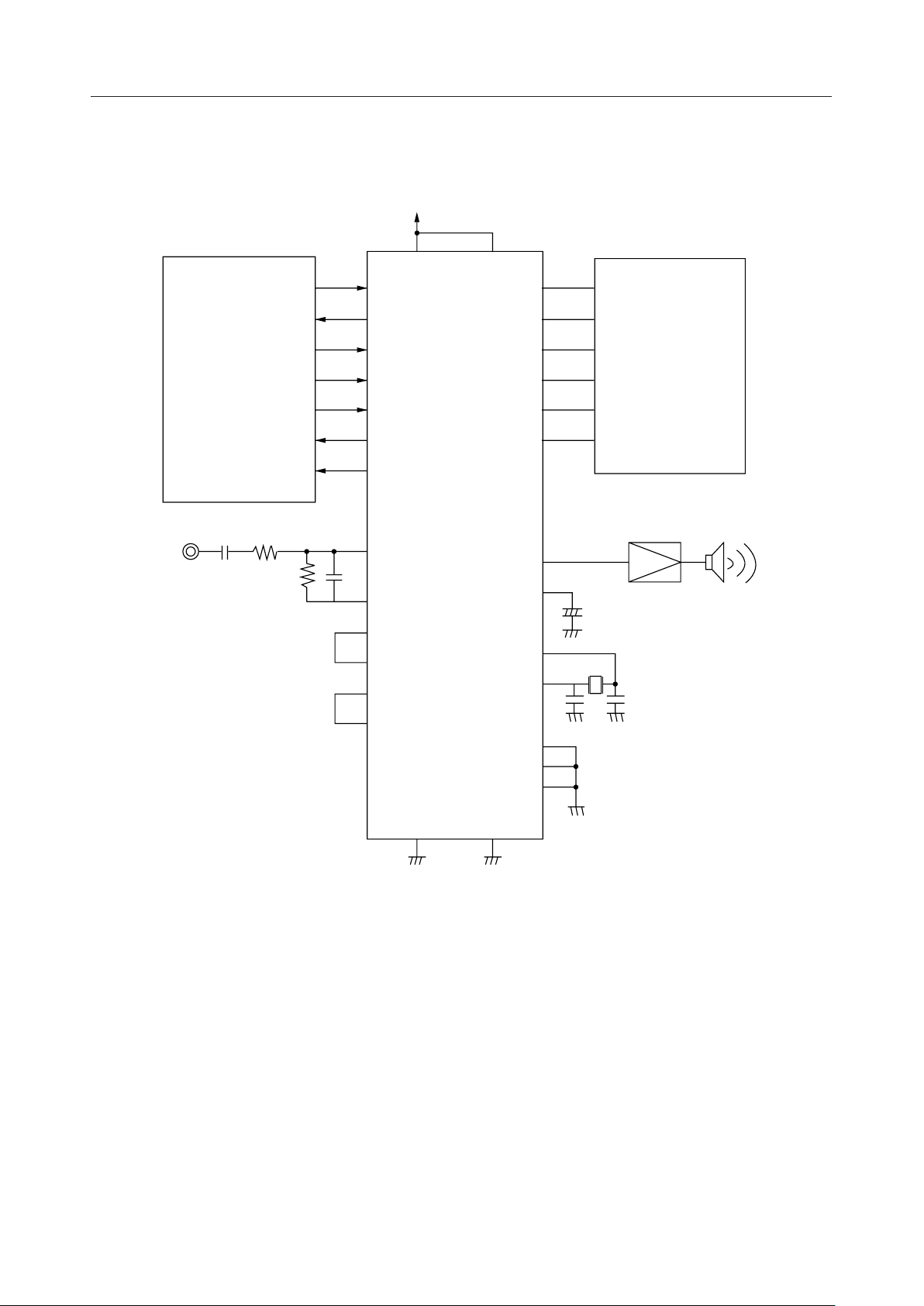
APPLICATION CIRCUITS EXAMPLE
MCU
Voice input
DV
DI
DO
SCK
CS
RESET
BUSY
MON
LIN
LOUT
AMON
FIN
FOUT
DD
AV
DD
FDI
FDO
FSCK
FCS
FRESET
FPRT
MSM9888L
AOUT
SG
XT
XT
DI
DO
SCK
CS
RESET
PRT
MSM9891L
MSM9892L
MSC1157
MSM9893L
ADIN
DGND AGND
TEST0
TEST1
TEST2
5/14
Page 6

¡ Semiconductor MSM9888L
COMMAND LIST
D6 D5 D4 D3 D2 D1 D0
Command
NOP
REC
PLY
STOP
PAUSE
BLKRW
DTRW
DEL
PDWN
BYTEW
BYTER
WEND
END
INIT
STATUS
C5 to C0 : Phrase No.
S2 to S1 : Sampling frequency
Pb to P0 : Page address on the flash memory
B8 to B0 : Block address on the flash memory
F1 to F0 : Type of flash memory connected
U7 to U0 : Number of user data blocks
D7
0000000
0
0010S2S1S0
0
0
0
010000M0
0
C6 C5 C4 C3 C2 C1 C0
C7
0110000
0
1000000
0
101000M1
0
D7 D6 D5 D4 D3 D2 D1 D0
1 1 0 Pb Pa P9 P8
0
P6 P5 P4 P3 P2 P1 P0
P7
1110000
0
0 C5C4C3C2C1C0
0
0000000
1
001000B8
1
B6 B5 B4 B3 B2 B1 B0
B7
W6 W5 W4 W3 W2 W1 W0
W7
010000B8
1
B7 B6 B5 B4 B3 B2 B1 B0
0110000
1
1000000
1
1101010
1
00000F1F0
0
U6 U5 U4 U3 U2 U1 U0
U7
1111111
1
C4 C3 C2 C1 C0
C5
Function
No function
Starts recording
Starts playback
Terminates recording/playback.
Pauses or resets pause.
Sets and reads the recording time.
Reads data from or writes data to the flash memory.
Erases phrases.
Stops the clock to select the power-down mode.
Writes the data written with W7-0 to the address
indicated by B8-0 to the flash memory buffer.
Reads data inside the buffer at the address indicated by
B8-0.
Writes buffer data to the flash memory then quits.
Quits without writing buffer data to the flash memory.
Initializes the voice area part of the flash memory.
Outputs the status.
X=don't care
6/14
Page 7

¡ Semiconductor MSM9888L
MODE0 setting
M0
0
1
Function
Flash playback
ROM playback
Channel designation
C7 C6 C5 C4 C3 C2 C1 C0
0
0
0
0
0
0
0
0
0
0
0
0
0
1
0
0
0
0
0
0
1
•
•
•
0
0
1
1
0
0
1
1
0
1
0
0
•
•
111111111
1
1
0
1
0
1
0
11111
•
•
•
1
1
0
•
•
Phrase1
1
Phrase2
0
Phrase3
1
•
•
•
Phrase59
1
Phrase63
1
Phrase64 (ROM only)
0
•
•
Phrase254 (ROM only)
Phrase255 (ROM only)
1
MODE1 setting
M1
0
Sets the number of blocks to be
record/played back with D7-0.
1
Sets the channel recorded with D7-0 and
outputs the recording time.
Function
Function
Page designation
Pb Pa P9 P8 P7 P6 P5 P4 P3 P2 P1 p0
000000000000
000000000001
000000000010
000000000011
•
•
•
111111111101
111111111110
111111111111
•
•
•
•
•
•
Function
Designates flash memory page 000h.
Designates flash memory page 001h.
Designates flash memory page 002h.
Designates flash memory page 003h.
•
•
•
Designates flash memory page FFDh.
Designates flash memory page FFEh.
Designates flash memory page FFFh.
7/14
Page 8

¡ Semiconductor MSM9888L
COMMAND DESCRIPTIONS
1) NOP
• Command
• Description Non-operation
2) REC
• Command
• Description Records the phrases designated by C7-C0 with the sampling frequency designated
00000000
No function available.
00010S2S1S0
C7 C6 C5 C4 C3 C2 C1 C0
by S2-S0.
• Others
Sampling frequency
S2
S1
S1
0
0
0
0
0
1
0
1
0
0
1
1
1
0
1
1
1
0
1
1
1
Function
2kHz
2.7kHz
3.2kHz
4kHz
5.3kHz
6.4kHz
8kHz
Phrase designation (1 to 63 phrases)
C7 C6 C5 C4 C3 C2 C1 C0
0
0
0
0
0
0
0
1
0
0
0
0
0
0
1
0
0
0
0
0
0
0
1
1
•
•
•
000011111
11110
1
•
•
•
1
Function
Phrase1
Phrase2
Phrase3
•
•
•
Phrase62
Phrase63
8/14
Page 9

¡ Semiconductor MSM9888L
3) PLY
• Command
• Description Plays back the phrases recorded on the flash memory when M0 is "0".
4) STOP
• Command
• Description Quits recording or playback.
0010000M0
C7 C6 C5 C4 C3 C2 C1 C0
Designate the phrases with C7-C0 (1 to 63 phrases).
Plays back the phrases in the mask ROM when M0 is "1".
Designate the phrases with C7-C0 (1 to 255 phrases).
00110000
5) PAUSE
• Command
• Description Pauses recording or playback.
6) BLKRW
• Command
Output
• Note Outputs O7-O0 only when M1 is "1".
• Description Designate the number of blocks to be recorded/played back withD7-D0 when
(1 to 63 phrases) designated with D7-D0.
• Blocks The entire flash memory is divided into 256 blocks.
01000000
Restarts recording or playback if the PAUSE command is input again.
0101000M1
D7 D6 D5 D4 D3 D2 D1 D0
O7 O6 O5 O4 O3 O2 O1 O0
M1 is "0". Outputs, using O7-O0, the number of blocks that recorded the phrases
One-block size =
Flash memory size
256
(bits)
9/14
Page 10

¡ Semiconductor MSM9888L
7) DTRW
• Command
0110PbPaP9P8
P7 P6 P5 P4 P3 P2 P1 P0
• Description Selects the DTRW mode. Inputs data to or outputs data from the flash memory
page designated with Pb-P0. To reset the DTRW mode, input the WEND
command or END command. The flash memory consists of 264 bytes per page.
The number of pages on each flash memory is as follows:
M9894L
8M
bits
33792
bits
4096
Pages
8) DEL
• Command
M9891L
Memory size
One-block size
Number of pages
01110000
C7 C6 C5 C4 C3 C2 C1 C0
1M
bits
4224
bits
512
Pages
M9892L
2M
bits
8448
bits
1024
Pages
M9893L
4M
bits
16896
bits
2048
Pages
• Description Erases the phrases designated with C7-C0 (flash memory only).
9) PDWN
• Command
10000000
• Description Stops the clock and sets the power-down mode after the command is input. To
reset the power-down mode, input RESET.
10) BYTEW
• Command
1001000B8
B7 B6 B5 B4 B3 B2 B1 B0
W7 W6 W5 W4 W3 W2 W1 W0
• Note This command is valid only in DTRW mode.
• Description Rewrites the content of the page designated with the DTRW command in units
of bytes. Designate the address in the page with B8-B0 and input data with W7W0.
10/14
Page 11

¡ Semiconductor MSM9888L
11) BYTER
• Command
1010000B8
B7 B6 B5 B4 B3 B2 B1 B0
Output
O7 O6 O5 O4 O3 O2 O1 O0
• Note This command is valid only in DTRW mode.
• Description Reads the content of the page designated with the DTRW command in units of
byte. When the address in the page is designated with B8-B0, data is output after
the command input.
12) WEND
• Command
10110000
• Note This command is valid only in DTRW mode.
• Description Writes the content of the page designated with the DTRW command to the flash
memory then exits the DTRW mode.
13) END
• Command
11000000
• Note This command is valid only in DTRW mode.
• Description Exits the DTRW mode without writing the content of the page designated with
the DTRW command to the flash memory.
11/14
Page 12

¡ Semiconductor MSM9888L
14) INIT
• Command
11101010
000000F1F0
U7 U6 U5 U4 U3 U2 U1 U0
• Description Initializes the area that eliminates the number of blocks designated with U7-U0)
from the end of the flash memory blocks as the recording/playback area. Also,
selects the type of the flash memory with F1-F0.
Block No..
00H
Voice area
0FFh - U + 1
F1 F0
00
01
10
11
0FFh - U
User area
0FFh
Flash memory size Product name
1Mbits MSM9891L
2Mbits MSM9892L
4Mbits MSM9893L
8Mbits MSM9894L
12/14
Page 13

¡ Semiconductor MSM9888L
15) STATUS
1111111
• Command
1
Output
O7 O6 O5 O4 O3 O2 O1 O0
• Description Outputs the M9888 status.
O7; MON
Outputs "1" during execution of the REC or PLY command. It includes the
memory management time in addition to the recording/playback time. Also,
outputs the same value as that of the MON pin.
O6; VPM
Outputs "1" during pause.
O5; RPM
Outputs "1" during actual recording by the REC command or during voice
output by the PLT command. Otherwise, "0" is output.
O3; MEMFUL
Outputs "1" when there is no voice area on the flash memory.
O2; NAR
Outputs "0" when the next phrase can be input during continuous voice
playback.
O4, O1, and O0 have no function.
13/14
Page 14

¡ Semiconductor MSM9888L
PACKAGE DIMENSIONS
(Unit : mm)
SSOP30-P-56-0.65-K
Mirror finish
Package material
Lead frame material
Pin treatment
Solder plate thickness
Package weight (g)
Epoxy resin
42 alloy
Solder plating
5 mm or more
0.19 TYP.
Notes for Mounting the Surface Mount Type Package
The SOP, QFP, TSOP, SOJ, QFJ (PLCC), SHP and BGA are surface mount type packages, which
are very susceptible to heat in reflow mounting and humidity absorbed in storage.
Therefore, before you perform reflow mounting, contact Oki’s responsible sales person for the
product name, package name, pin number, package code and desired mounting conditions
(reflow method, temperature and times).
14/14
 Loading...