

Page 1

E2F0007-18-11
Preliminary
This version: Jan. 1998
MSM9405¡ Semiconductor
¡ Semiconductor
MSM9405
IrDA Communication Controller
GENERAL DESCRIPTION
The MSM9405 is a communication controller conforming to IrDA, the international standard for
infrared data communication. The device covers the IrDA physical specifications Ver.1.0 and
1.1.
Since the device performs some of the functions concerning communication protocol control,
the load on the software (firmware) for protocol control can be reduced. By combining the
device with another microcontroller and an infrared transceiver module, a device provided
with IrDA-compliant communication function can be configured.
FEATURES
• Data transfer rates
IrDA 1.0 : 2400, 9600 bps; 19.2, 38.4, 57.6, 115.2 kbps
IrDA 1.1 : 0.576, 1.152, 4 Mbps
• Detection/removal for beginning of frame and end of frame (IrDA 1.0, 1.1)
Insertion for beginning of frame and end of frame (IrDA 1.0, 1.1)
• Generation/check for CRC (IrDA 1.0, 1.1)
• Host interface
8-bit data bus : D0-D
DMA transfer : DREQ, DACK, TC
Interrupt : INTR
Address : A0-A
Control signal : CS, RD, WR
• Infrared module control signal : SD
• Built-in 32-byte transmit-receive FIFOs
• Power down mode
• Built-in oscillator circuit
7
3
• Crystal oscillation frequency : 18.432 MHz (other than 4 Mbps data rate)
: 48 MHz (when 4 Mbps data rate used)
• Operating voltage (VDD) : 2.7 to 3.6 V
• Package:
30-pin plastic SSOP (SSOP30-P-56-0.65-K) (Product name : MSM9405MB)
1/30
Page 2
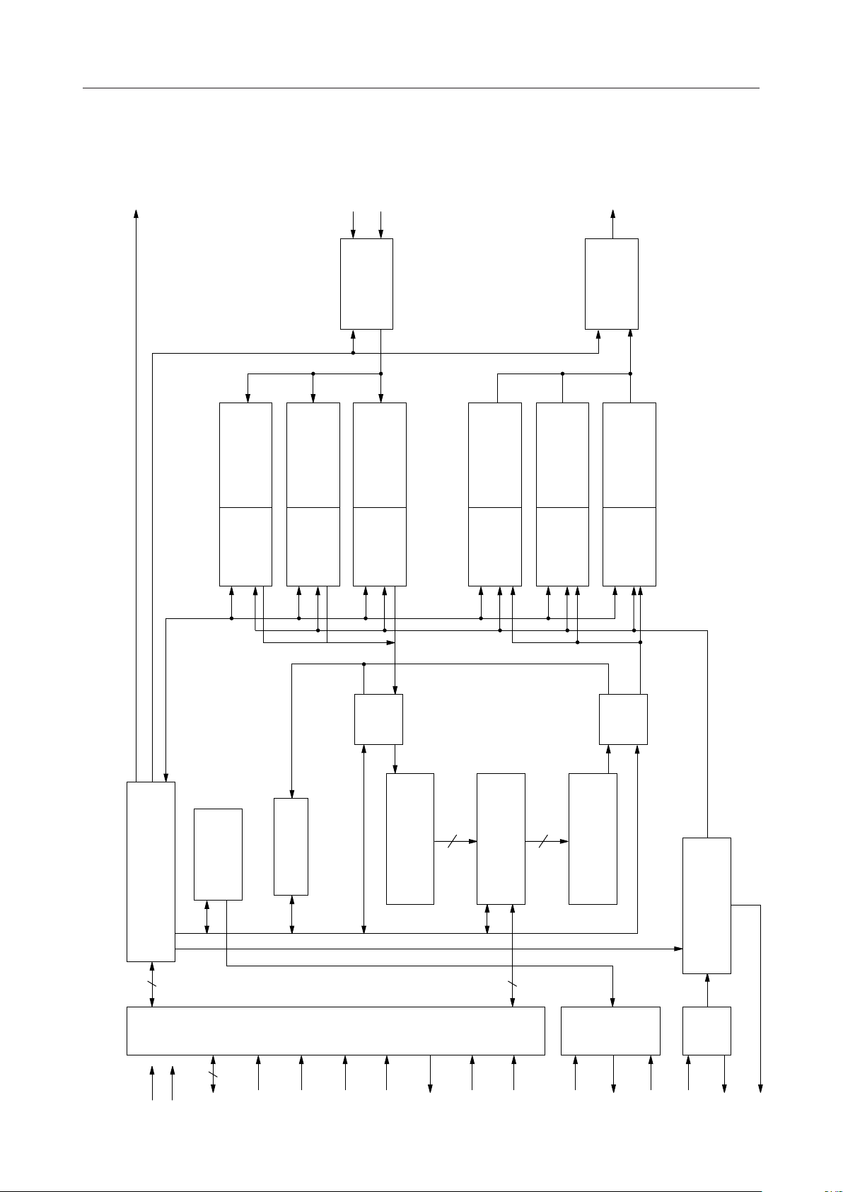
BLOCK DIAGRAM
SD
IRIN-A
IRIN-B
MSM9405¡ Semiconductor
IROUT
DEC
UART
Flag Detection/
Removal Circuit
IrDA
Flag Detection/
Removal Circuit
DEC
HDLC-
Demodulator
Removal Circuit
Preamble/Flag Detection/
DEC
4 PPM-
ENC
UART
Circuit
Flag Insertion
IrDA
Modulator
Flag Insertion Circuit
ENC
HDLC-
Preamble/Flag/
4 PPM-
Insertion Circuit
ENC
Register
Control/Status
8
DD
V
GND
DMA
Control Circuit
8
0-7
D
TCC/RCC
Microcontroller I/F
0-3
A
CS
RD
RX_
CRC
WR
Receive Shift
Register (RSR)
INTR
8
(32¥8bit)
Transmit-Receive FIFO
8
PWDN
RESET
8
(TSR)
Transmit Shift Register
DMA
TC
TX_
I/F
DREQ
CRC
DACK
Generator
Baud Rate
OSC
XIN
XOUT
TEST
2/30
Page 3
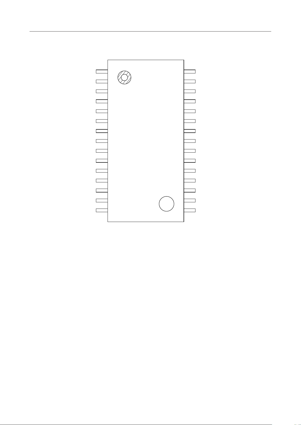
PIN CONFIGURATION (TOP VIEW)
MSM9405¡ Semiconductor
V
DD
D
D
D
D
D
D
D
D
A
A
A
A
CS
RD
1
2
7
3
6
4
5
5
4
6
3
7
2
8
1
9
0
10
3
11
2
12
1
13
0
14
15
30
XIN
29
XOUT
28
TEST
27
IRIN-A
26
IRIN-B
25
IROUT
24
SD
23
TC
22
DREQ
21
DACK
20
PWDN
19
RESET
18
INTR
17
WR
16
GND
30-Pin Plastic SSOP
3/30
Page 4

PIN DESCRIPTIONS
MSM9405¡ Semiconductor
Transceiver
Module Interface
Microcontroller
Interface
DMA Controller
Interface
Others
27
26
25
9-2
13-10
14
15
17
18
22
21
23
20
19
Type
IRIN-A I
IRIN-B I
IROUT O
SD O24
D0-D
A0-A
I/O
7
3
CS
RD I
WR I
INTR O
DREQ O
DACK
TC I
PWDN I
RESET I
DescriptionSymbolPinFunction
Receive signal input A. (2.4 kbps to 4 Mbps)
*1
Receive signal input B. (0.576 to 4 Mbps)
When connecting this device to a transceiver module,
tie this pin high or low if the number of the receive signal
output pins that the module has is only one.
*1
Transmit signal output. Active high.
Transceiver module control signal output.
Becomes active when PWDN is set low.
*1
This pin must be left open if connecting this device to a
transceiver module having no shutdown pins.
Data input-output.
I
Register address inputs.
I
Chip select input. Active low.
When low, read and write signals are enabled.
Read signal input. Active low.
Write signal input. Active low.
Interrupt request signal output. Active low.
DMA Request signal output.
I
DMA acknowledge signal input.
*1
*1
DMA transfer end signal input. Active low.
Power down control. Active low.
When set low, oscillation stops and the device enters power
down (low supply current) mode.
System reset input. Active low.
When set low, the internal registers are initialized.
28
30
29
1
16
TEST O
XIN I
XOUT O
V
DD
—
GND —
Test. Must be left open.
Crystal connect.
Crystal connect.
Power supply.
Ground.
*1 Either active high or active low can be selected depending on the register setting.
4/30
Page 5
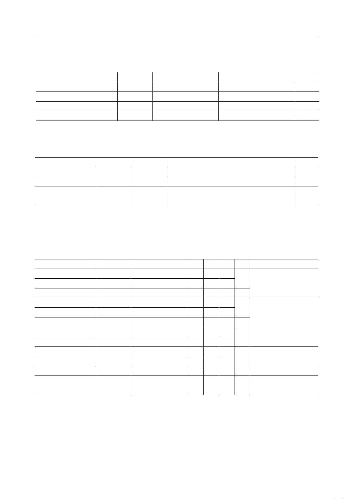
ABSOLUTE MAXIMUM RATINGS
Parameter Symbol Condition Rating Unit
Supply Voltage V
Input Voltage V
Power Dissipation P
Storage Temperature T
DD
I
D
STG
— –0.5 to +4.0 V
— –0.5 to +6.0 V
— 230 mW
— –55 to +150 °C
RECOMMENDED OPERATING CONDITIONS
Parameter Symbol Condition Range Unit
Supply Voltage V
Operating Temperature T
Crystal Oscillation
Frequency
f
OSC
DD
op
— 2.7 to 3.6 V
— –20 to +70 °C
— 18.432 MHz ±200 ppm or 48 MHz ±100 ppm —
MSM9405¡ Semiconductor
ELECTRICAL CHARACTERISTICS
DC Characteristics
= 2.7 to 3.6 V, Ta = –20 to +70°C)
(V
DD
Parameter Symbol Condition Applicable Pin
"H" Input Voltage V
"L" Input Voltage V
Input Leakage Current I
"H" Input Voltage V
"L" Input Voltage V
Input Leakage Current I
"H" Output Voltage V
"L" Output Voltage V
"H" Output Voltage V
"L" Output Voltage V
Supply Current I
IH
IL
LI
IH
IL
LI
OH
OL
OH
OL
DD
— IRIN-A, IRIN-B, PWDN
—A
VI = VDD/0 V TC, RESET, DACK
—
—
VI = VDD/0 V
IO = –4 mA
IO = 4 mA — — 0.4
IO = –4 mA 2.4 — —
IO = 4 mA — — 0.4
———20 V
Supply Current
(during Power Down)
I
DPN
When PWDN = "L" — — — V
Min.
2.2
0
—
2.2
0
—
2.4
Typ.
—
—
—
—
—
—
—
Max.
5.5
*1
0.8
±1
5.5
*1
0.8
±10—mA
Unit
V
mA
V
V
V
mA
mA
0-A3
IROUT, INTR, DREQ
, CS, RD, WR,
D
0-D7
DD
DD
*1 1.0 V when V
= 3.0 to 3.6 V
DD
5/30
Page 6

AC Characteristics
Parameter Symbol Condition Note
Read Pulse Width t
Read Data Delay Time t
Read Data Hold Time t
Read/Write Recovery Time t
CS Setup Time t
CS Hold Time t
Write Address Hold Time t
Write Pulse Width t
Write Data Setup Time t
Write Data Hold Time t
Write Address Setup Time t
Interrupt Clear Time t
DACK Pulse Width t
DACK Setup Time t
DREQ Clear Time t
DACK Hold Time (during Read) t
DACK Hold Time (during Write) t
TC Pulse Width t
TC Setup Time t
TC Hold Time t
SIR Pulse Width t
SIR Data Rate Tolerance SDRT
MIR Pulse width t
MIR Data Rate Tolerance MDRT
FIR Single Pulse Width t
FIR Data Rate Tolerance FDRT
FIR Double Pulse Width t
Reset Pulse Width t
rpw
rdd
rdh
rcv
css
csh
wah
wpw
wds
wdh
was
intr
dak
acs
drqr
achr
achw
tcw
tcs
tch
spw
mpw
fpw
fdpw
rstw
= 2.7 to 3.6 V, Ta = –20 to +70°C)
(V
DD
Min.
—
— *2
— *3
120/70
—
0
Typ.
—
—
—
Max.
—
60
20
Unit
ns
ns
ns
—ns——60
—ns——60
—ns——0
—ns——0
—ns——120/70
—ns——60
—ns——–10
—ns——–10
—ns120/70——
—ns——60
—ns——10
—ns120/70——
—ns——–5
—ns——10
—ns——50
—ns——0
—ns——0
Transmitter ms—1.63—
Receiver ms——0.9
Transmitter %±0.87——
Receiver %±2.0——
Transmitter ns—218—
Receiver ns——100
Transmitter %±0.1——
Receiver %±0.2——
Transmitter ns—125—
Receiver ns165—70
Transmitter %±0.01——
Receiver %±0.1——
Transmitter ns—250—
Receiver ns285—195
—ns——70
MSM9405¡ Semiconductor
*1
*1
*1
*1
*1 120 ns when crystal oscillation frequency = 18.432 MHz,
70 ns when crystal oscillation frequency = 48 MHz
*2 That which occurs latest of the following is to be used for the data delay time (t
the change of the state of A0-A3, the change from CS high to low, and the change from
RD high to low.
*3 That which occurs first of the following is to be used for the read data hold time (t
the change of the state of A0-A3, the change from CS low to high, and the change from
RD low to high.
rdd
rdh
6/30
) :
) :
Page 7

• Read timing
MSM9405¡ Semiconductor
t
rdd
CS
A
RD
D
0-A3
-D
0
t
rpw
t
rdd
t
rpw
t
rpw
t
rdd
7
t
rdh
t
rdh
t
rdh
t
rcv
INTR
t
intr
7/30
Page 8
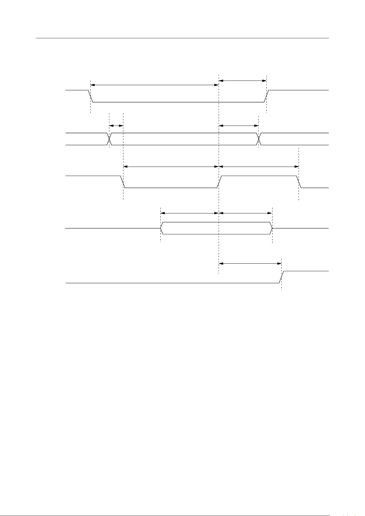
• Write timing
CS
t
css
t
MSM9405¡ Semiconductor
csh
A
0-A3
WR
D
0-D7
INTR
t
was
t
wpw
t
wds
t
wah
t
wdh
t
intr
t
rcv
8/30
Page 9
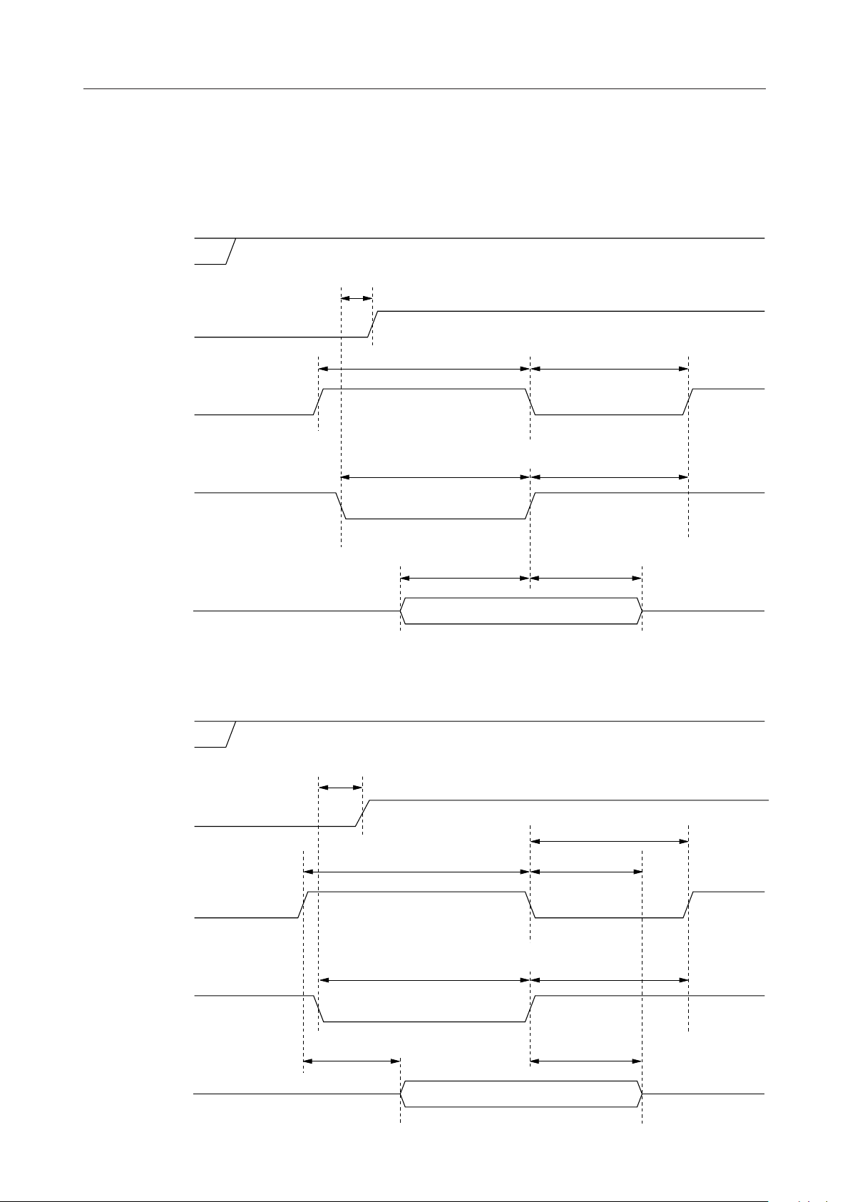
• DMAC access timing 1
DMA_EN = "1", DMA_SL1 = "0", DMA_SL0 = "0"
MemoryÆM9405
CS
DREQ
(Active low)
DACK
t
drqr
MSM9405¡ Semiconductor
t
dak
t
rcv
RD
D
0-D7
M9405ÆMemory
CS
DREQ
(Active low)
t
drqr
t
t
rpw
dak
t
wds
t
wdh
t
rdh
t
rcv
t
rcv
DACK
WR
D
0-D7
t
wpw
t
rdd
t
rcv
t
rdh
9/30
Page 10
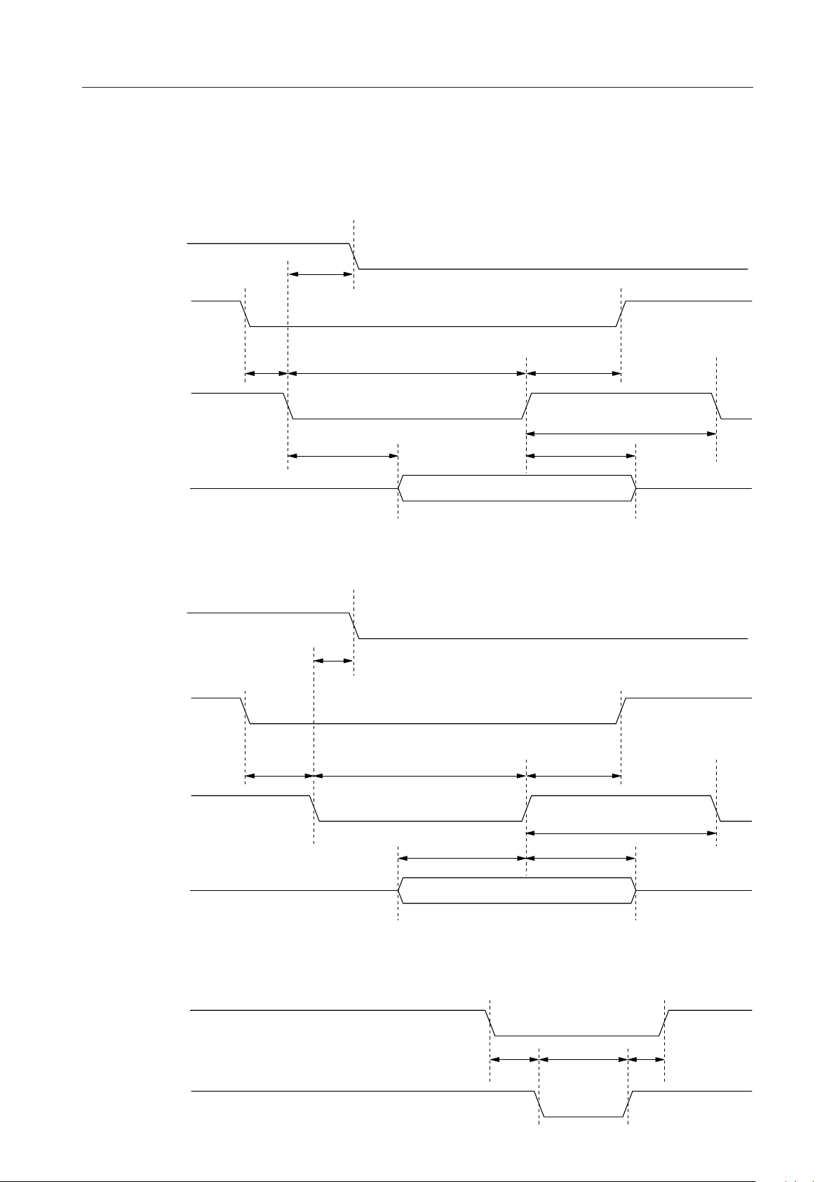
• DMAC access timing 2
DMA_EN = "1", DMA_SL1 = "0", DMA_SL0 = "1"
M9405ÆMemory
MSM9405¡ Semiconductor
DREQ
(Active high)
DACK
RD
D
0-D7
MemoryÆM9405
DREQ
(Active high)
t
acs
t
drqr
t
t
drqr
rdd
t
rpw
t
achr
t
rcv
t
rdh
DACK
WR
D
0-D7
WR
TC
t
acs
t
wpw
t
wds
t
achw
t
rcv
t
wdh
t
tcs
t
tcw
t
tch
10/30
Page 11
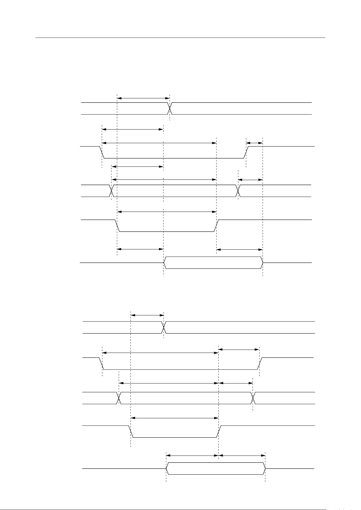
• DMAC access timing 3
DMA_EN = "1", DMA_SL1 = "1", DMA_SL0 = "1" or "0"
M9405ÆMemory
t
drqr
DREQ
t
rdd
CS
t
rdd
A
0-A3
t
t
t
rpw
rpw
rpw
MSM9405¡ Semiconductor
t
rdh
t
rdh
RD
D0-D
7
MemoryÆM9405
DREQ
CS
A
0-A3
t
t
t
wah
rdh
csh
t
rdd
t
drqr
t
css
t
was
WR
D0-D
t
wpw
t
wds
7
t
wdh
11/30
Page 12
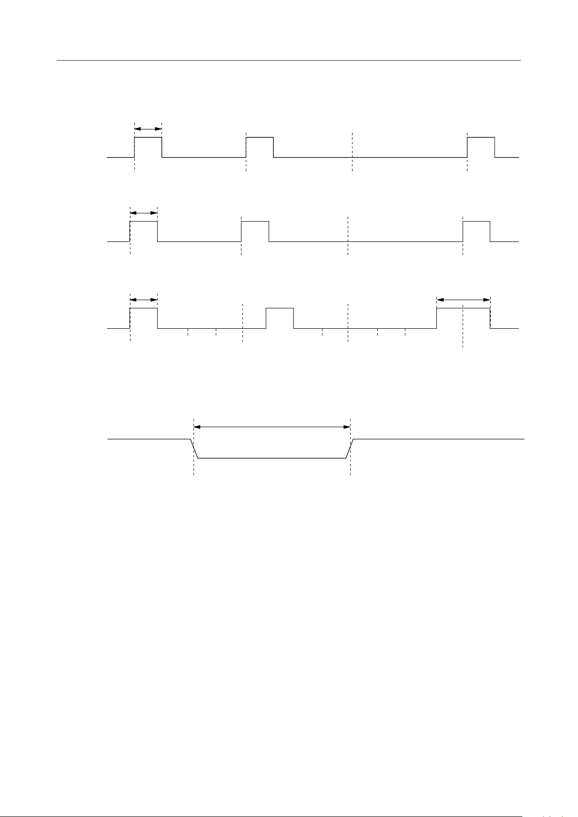
• Infrared interface timing
t
spw
SIR
t
mpw
MIR
MSM9405¡ Semiconductor
FIR
• Reset timing
RESET
t
fpw
t
rstw
t
fdpw
12/30
Page 13
MSM9405¡ Semiconductor
FUNCTIONAL DESCRIPTION
Modes
There are four modes provided by the MSM9405 for IrDA communication. Communication
with IrDA1.0 is in SIR mode or Extended-SIR mode, while communication with IrDA1.1 is in
MIR mode or FIR mode. In SIR mode, the MSM9405 has the necessary UART feature for IrDA
communication. The Extended-SIR mode is an original feature of the MSM9405. In this mode,
BOF/EOF insertion and CRC calculation/check are performed by the MSM9405. Therefore, the
burden to the CPU can be reduced compared with IrDA1.0 communication using ordinary
UART. Moreover, the Extended-SIR mode allows DMA transfer even in IrDA1.0 communication.
In MIR mode, IrDA1.1 communication at up to 1.152 Mbps is possible. The FIR mode supports
4 Mbps transfer for IrDA1.1. Features of each mode are as follows:
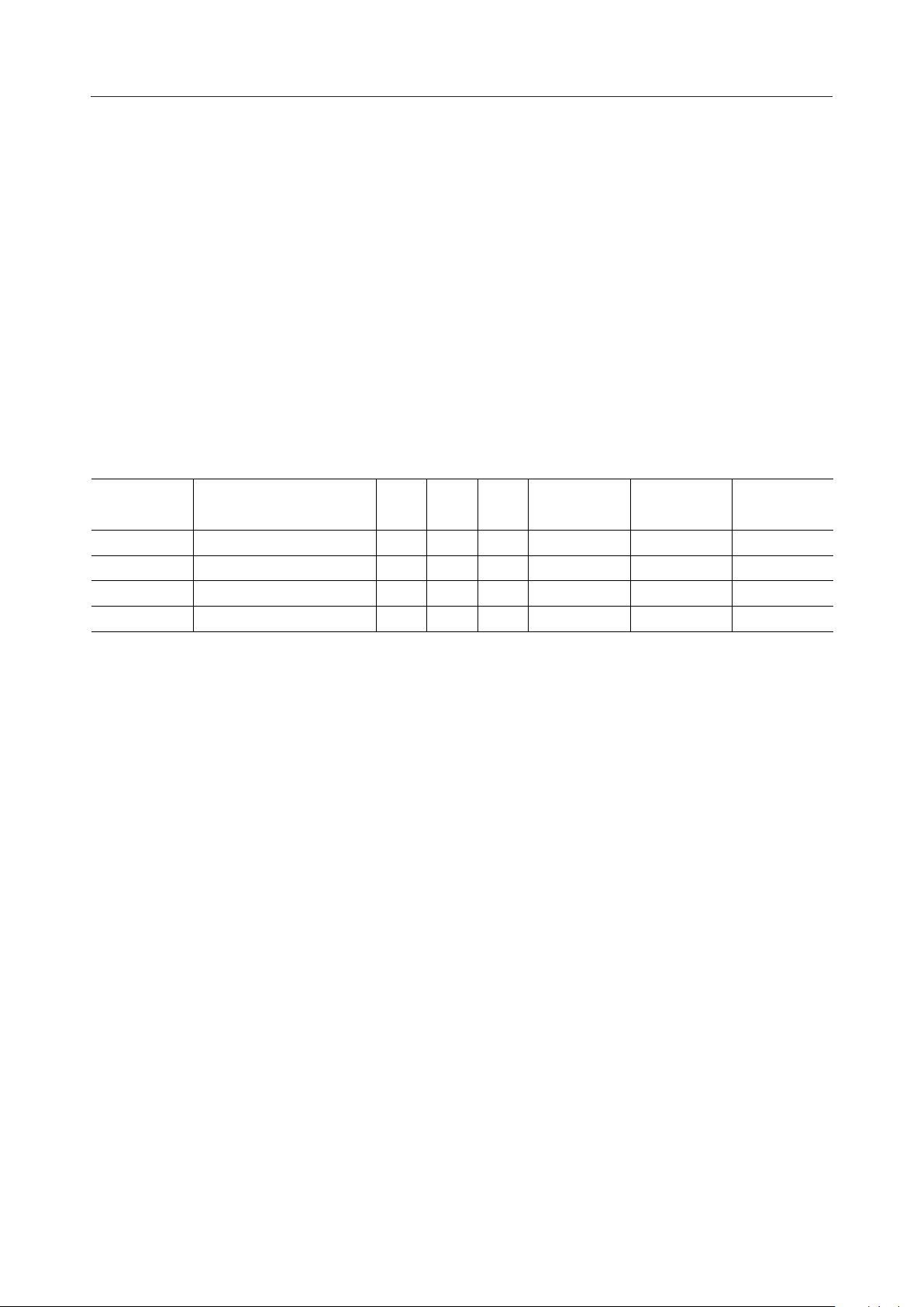
MSM9405 Modes Comparison
mode Transfer rate
EOFCRCBOF
CE insertion/
removal
"0" insertion/
removal
CE : Control Escape Byte
SW : Software
HW : Hardware
Preamble
insertion/removal
——SWSWSWSWSIR 2.4 to 115.2 kbps
——HWHWHWHWExtended-SIR 2.4 to 115.2 kbps
—HW—HWHWHWMIR 0.576, 1.152 Mbps
HW——HWHWHWFIR 4 Mbps
Sending/Receiving Switching Method
Mode switching between sending and receiving is made using the TX_EN and RX_EN bits in
the ICR1 (Infrared Control Register 1). For sending, writing "1" in TX_EN puts the MSM9405
in the sending mode. Writing "1" in RX_EN puts the MSM9405 in the receiving mode. If "0" is
written to both TX_EN and RX_EN bits, the MSM9405 does not perform sending/receiving but
enters the idle state. Each register can be set even during the idle state. Data to be sent can be
written in advance to the FIFO during the idle state.
If "1" is written to both TX_EN and RX_EN, the MSM9405 is put in the receiving mode.
DMA Transfer
The MSM9405 allows DMA transfer. The DMA transfer mode covers the single transfer mode
and demand transfer mode, but not the block transfer mode. When a DMA controller with TC
output is used for sending, the DMA controller and MSM9405 automatically perform highspeed transfer if the maximum frame length is specified for TFL and the transfer data length for
the TC counter of the DMA controller.
The timing when the DREQ signal is asserted is as follows:
During receiving, DREQ is asserted when data in the FIFO is at or above the receiving threshold
level or time-out occurs.
If all of the received data in the FIFO is read, DREQ is deasserted.
During sending, DREQ is asserted when data in the FIFO is lower than the sending threshold
level. Sent data is written and DREQ is deasserted when the FIFO becomes full or TXE_EV
occurs.
13/30
Page 14

MSM9405¡ Semiconductor
Time-out
The MSM9405 outputs an interrupt request or DMA request depending on the register setting
when the following time-out occurs even if the received data is below the receiving threshold
level:
The condition causing time-out in MIR or FIR mode is:
At least 1-byte data is in the receiving FIFO and 69.5 ms has passed after data is written from
the receiving shift register to the FIFO. During this period, the CPU or DMA controller does
not read the FIFO data.
The condition causing time-out in SIR or Extended SIR mode is:
At least 1-byte data is in the receiving FIFO and time (Tout) has passed after data is written
from the receiving shift register to the FIFO. During this period, the CPU or DMA controller
does not read the FIFO data.
Tout = 4 ¥ 8 ¥ 1/baud rate
baud rate: Transfer rate (2.4 to 115.2 kbps)
Register Map
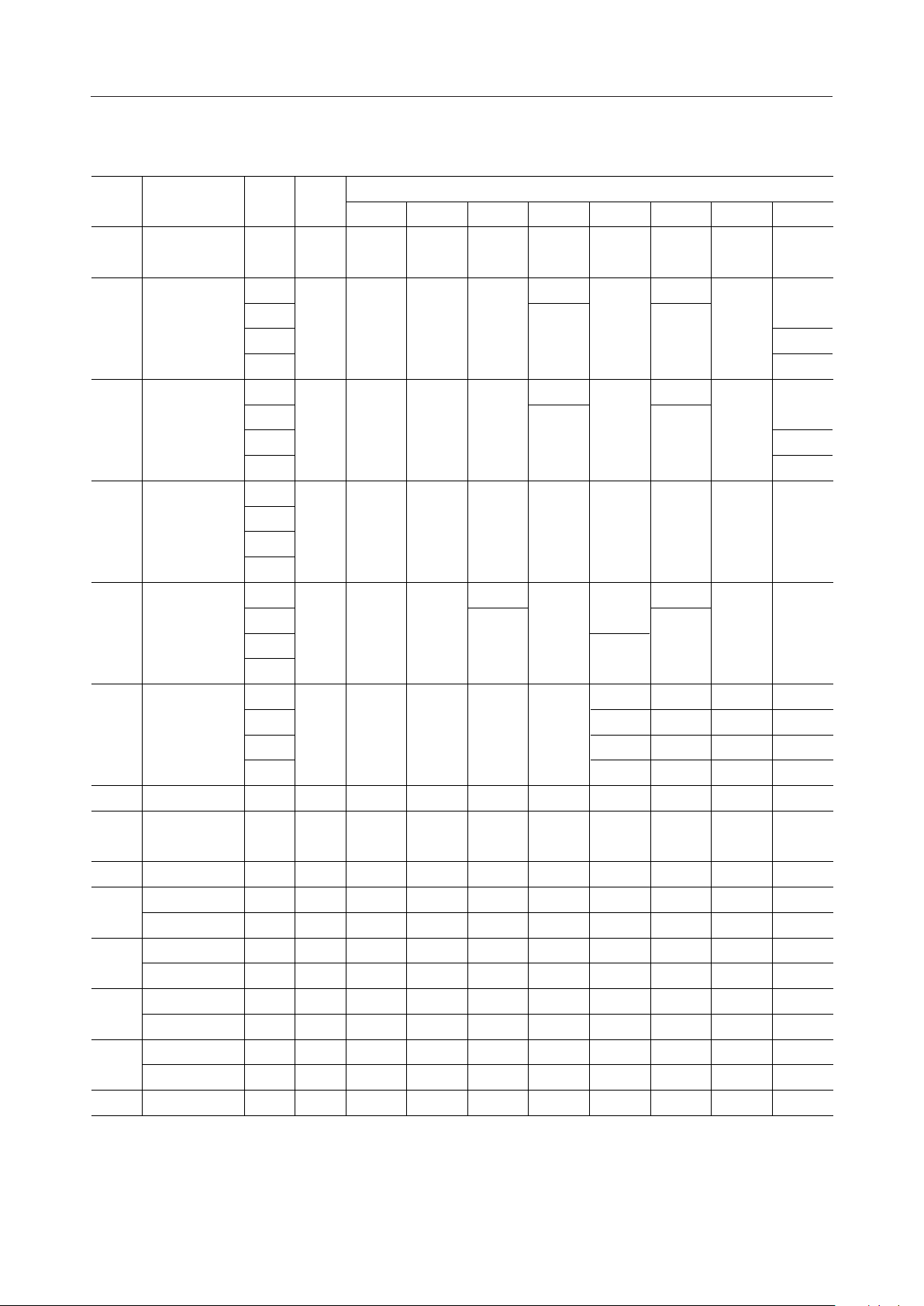
The MSM9405 contains 14 registers, of which 13 are available. Each register can be selected with
the register address assigned from 0h through Ch. Various setting options are provided for each
register to allow optimum communication.
The registers are listed below. The register table is given on the next page.
A3-A
0h
1h R/W ENR Interrupt enable register
2h R EIR Interrupt event and status indication register
3h R LSR Status register
4h R/W ICR1 Transmit-receive control register
5h R/W ICR2 BOF count setting register
6h R/W MSR Register for setting a transfer mode and a data rate and selecting a
7h R/W DSR DMA mode setting register
8h R/W FCR FIFO threshold setting register
9h R/W TFL (L) Transmit frame-length setting register (low-order byte)
Ah R/W TFL (H)
9h R TCC (L) Transmitter current-count register (low-order byte)
Ah R TCC (H)
Bh R/W MDS (L) Maximum data size setting register (low-order byte)
0h R/W MDS (H)
Bh R RST (L) Receiver frame length stack register (low-order byte)
Ch R RST (H)
Fh R/W TEST Used for test.
R/W Register Name
0
R RDR Receive data register
W TDR Transmit data register
Description
crystal to be used
1
*
Transmit frame-length setting register (high-order byte)
1
*
1
*
Transmitter current-count register (high-order byte)
*1
*2
Maximum data size setting register (high-order byte)
*2
*2
Receiver frame length stack register (high-order byte)
*2
*1 Whether TFL or TCC is read depends on the setting of the CTEST bit in the MSR
register.
*2 Whether MDS or RST is read depends on the setting of the CTEST bit in the MSR
register.
14/30
Page 15
Register Table
MSM9405¡ Semiconductor
Register
name
R/WModeAdd
R/Wall0 TDR/RDR
/RDR
TDR
TDR
7
/RDR
7
SIR
Ex-SIR
1 ENR TXL_IE
TXE_IER/W
MIR
FIR
SIR
Ex-SIR
2 EIR TXL_EV
TXE_EVR
MIR
FIR
SIR
Ex-SIR
FLV
3 LSR
MIR
R
FLV
5
4
FIR
SIR
Ex-SIR
4 ICR1
MS_ENR/W
TCC_EN
MIR
FIR
SIR
Ex-SIR
5 ICR2
CTESTR/W
SD_INV
MIR
FIR
R/W6 MSR all DRS
DRS
2
*R/W7 DSR all ****
R/W8 FCR all RXTH2RXTH1RXTH0TXTH3TXTH2TXTH1TXTH
TFL (L) all TFL
R/W
9
TFL (H) all ***TFL11TFL
RXTH
3
TFL
7
TCC
RTCC (L) all TCC
7
*R/W
6
A
*RTCC (H) all * * * TCC
MDS (L) all
R/W
MDS
B
RST
RRST (L) all
MDS (H) all ***MDS11MDS
MDS
7
RST
7
*R/W
C
*RRST (H) all * * * RST
F
R/WTEST all TEST6TEST5TEST4TEST3TEST2TEST1TEST
TEST
7
Function of each bit
TDR
6
/RDR
6
TDR
5
/RDR
5
*
TDR
4
/RDR
4
TDR
3
/RDR
3
TDR
2
/RDR
2
*
RXH/T
_IE
EOF_IE CE_IE
MLE_IE
*
OE_IE
*
RXH/T
_EV
FLV
EOF_EV CE_EV
MLE_EV
FLV
3
FLV
2
*
FLV0IR_DET TOUT
1
OE_EV
*
*
CRC_
INV
FCLR
S_EOT
IR_PLS
RX_EN TX_EN
****
IRIN
_SL
RXINV
SBF
MBF
SBF
3
MBF
3
SBF
2
MBF
2
****
DRS0XT_SL * * IRSL1IRSL
1
DMA_
SL
TFL
TCC
6
MDS5MDS4MDS3MDS2MDS1MDS
6
RST
6
TFL
5
TCC
5
RST
5
TFL
4
TCC
4
RST
4
3
11
11
TFL
TCC
3
TCC
RST
3
RST
DMA_
1
TFL
2
TCC
2
TFL
10
TCC
10
RST
2
MDS9MDS
10
RST
10
SL
0
1
1
1
1
1
1
9
9
1
9
Bit0Bit1Bit2Bit3Bit4Bit5Bit6Bit7
TDR
/RDR
FE_IE
AS_IE
ECE_IE
FE_EV
AS_EV
ECE_EV
SBF
0
MBF
DMA_
EN
TFL
0
TCC
0
TFL
8
TCC
8
RST
0
RST
8
0
0
0
0
0
0
8
0
15/30
Page 16
MSM9405¡ Semiconductor
(
)
Registers
• TDR: Transmit Data Register (Write Only)
RDR: Receive Data Register (Read Only) (Address = 0h)
The TDR (Transmit Data Register) and RDR (Receive Data Register) are used to read/write data
directly upon receiving/sending the data. The TDR and RDR share the same address. When
data is written in the sending mode or during the idle state, the TDR works as the top of the FIFO
and 1-byte data can be written to the FIFO. When data is read in the receiving mode, the RDR
works as the bottom of the FIFO and 1-byte data in the FIFO can be read. Serial-to-parallel
conversion is performed by the RSR. Parallel-to-serial conversion is performed by the TSR.
Reading from the TDR or writing to the RDR is invalid. The contents of the FIFO and TDR/RDR
are cleard by writing "1" to FCLR in the ICR1 register. The TSR and RSR cannot be cleared.
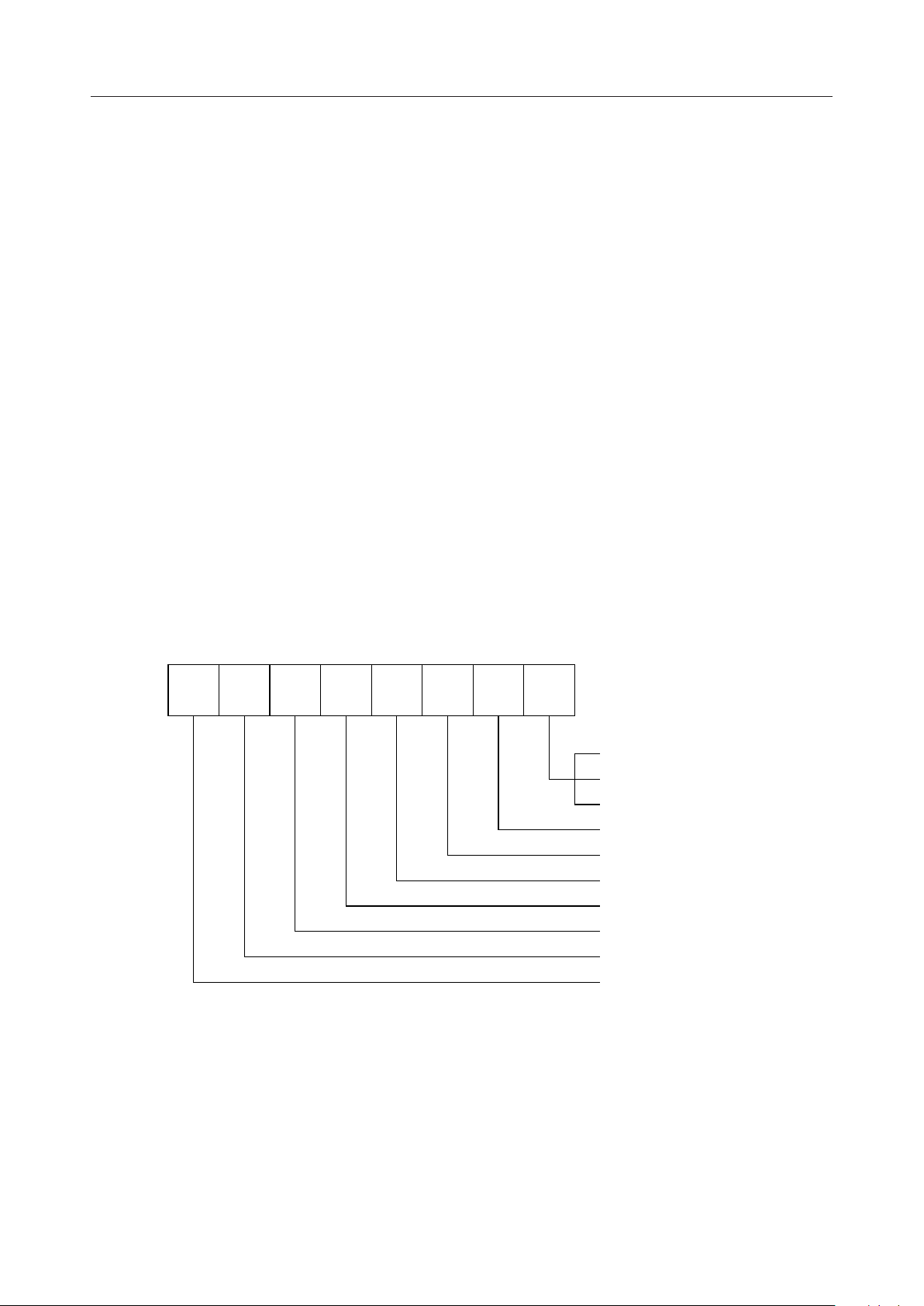
• ENR: Enable Register (Address = 1h)
The ENR (Enable Register) is used to control enabling/disabling various interrupts on the
MSM9405. Each of eight bits corresponds to each of eight interrupts provided on the MSM9405.
Each of eight interrupts can be independently controlled by each bit. When the system is reset,
all bits are reset to "0". By writing "1" to the bit corresponding to the desired interrupt, the
specified interrupt is enabled.
ENR7ENR6ENR5ENR4ENR3ENR2ENR1ENR
0
FE_IE (Enable = "1")
AS_IE (Enable = "1")
ECE_IE (Enable = "1")
OE_IE (Enable = "1")
CE_IE (Enable = "1")
MLE_IE (Enable = "1")
EOF_IE (Enable = "1")
RXH/T_IE (Enable = "1")
TXL_IE (Enable = "1")
TXE_IE
Enable = "1"
16/30
Page 17

MSM9405¡ Semiconductor
ENR bit
ENR[0]
ENR[1]
ENR[2]
ENR[3]
ENR[4]
ENR[5]
ENR[6]
ENR[7]
Table bit
This bit works as FE_IE in SIR or Extended-SIR mode, as AS_IE in MIR mode, and as ECE_IE in FIR
mode.
- FE_IE (Framing Error Interrupt Enable) (SIR mode/Extended-SIR mode): This bit enables/disables
interrupt when an FE (Framing Error : Stop bit not detected) has occurred.
- AS_IE (Abort Sequence Interrupt Enable) (MIR mode): This bit enables/disables interrupt when
an abort sequence has been received.
- ECE_IE (Encode Error Interrupt Enable) (FIR mode): This bit enables/disables interrupt when an
encode error has occurred.
OE_IE (Overrun Error Interrupt Enable) : This bit enables/disables interrupt when an OE (Overrun
error : Error that occurs when the FIFO is full upon receiving and the next character is completely
received by the RSR) has occurred.
CE_IE (CRC Error Interrupt Enable) : This bit enables/disables interrupt when a CE (CRC Error) has
occurred. This bit is valid in either Extended-SIR, MIR, or FIR mode. In SIR mode, this bit must
be set to "0" (disable).
MLE_IE (Maximum Length Error Interrupt Enable) : This bit enables/disables interrupt when an MLE
(Maximum Length Error: Error that occurs when a frame exceeding the maximum data size set by
the MDS is received) has occurred.
EOF_IE (End Of Frame Interrupt Enable) : This bit enables/disables interrupt when the last byte in
the frame's data field has been detected in either Extended-SIR, MIR, or FIR mode. In SIR mode,
this bit must be set to "0" (disable).
RXH/T_IE (Receiver High-Data-Level/Timeout Interrupt Enable) : This bit enables/disables interrupt
when the received data is at or above the receiving threshold level or time-out has occurred.
TXL_IE (Transmitter Low-Data-Level Interrupt Enable) : This bit enables/disables interrupt when the
sent data is below the sending threshold level.
TXE_IE (Transmitter Empty Interrupt Enable) : This bit enables/disables interrupt when both the
FIFO and the TSR have become empty upon sending.
17/30
Page 18
MSM9405¡ Semiconductor
(
)
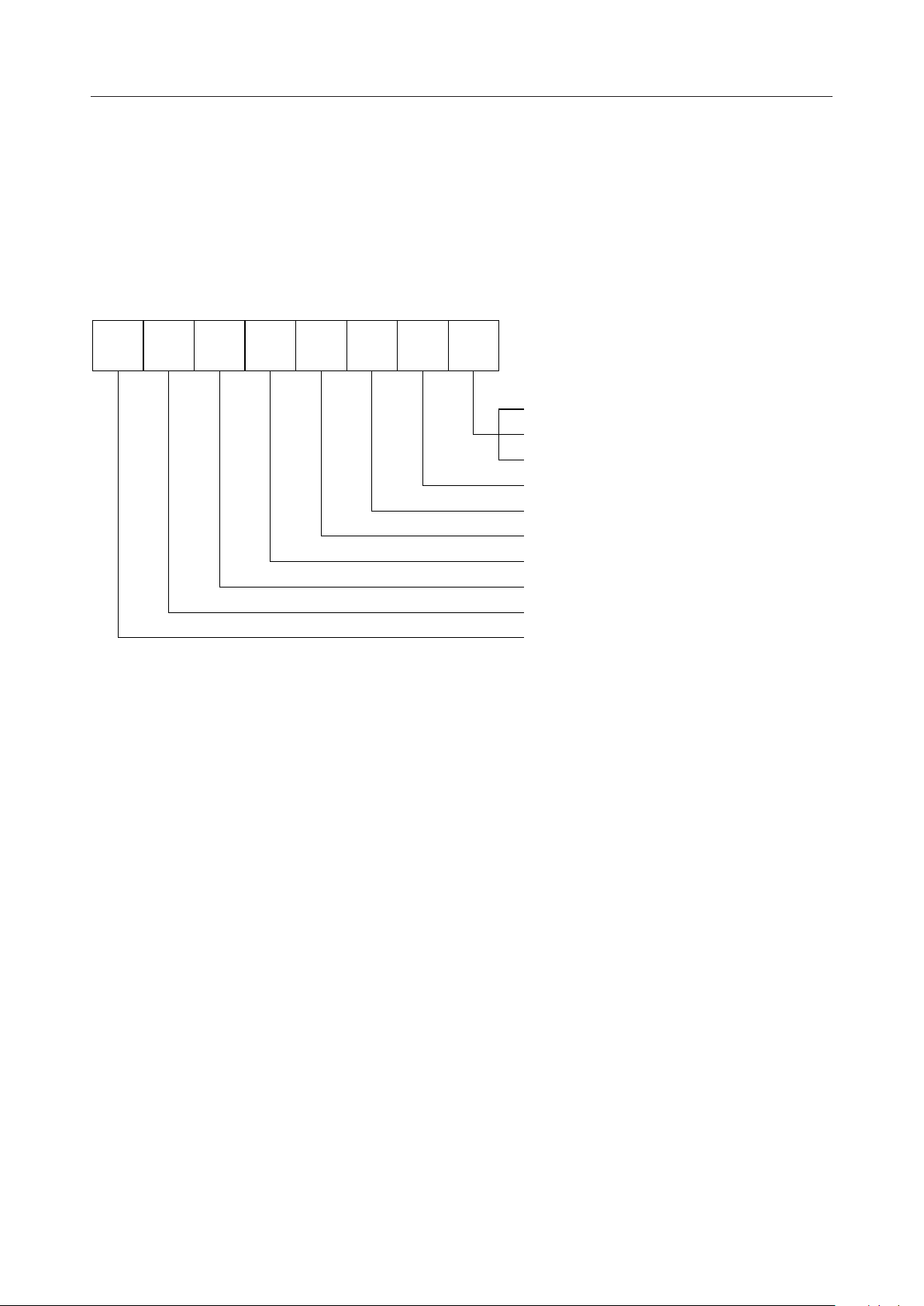
• EIR: Event Identification Register (Read Only) (Address = 2h)
The EIR (Event Identification Register) indicates factors of various interrupts on the MSM9405.
Each of eight bits corresponds to each interrupt bit assignment set on the ENR. The EIR works
as the status register even if the interrupt is disabled. When an event occurs, each corresponding
bit is set to "1". When the system is reset, all bits are reset to "0".
EIR7EIR6EIR5EIR4EIR3EIR2EIR1EIR
0
FE_EV (Framing Error = "1")
AS_EV (Abort Sequence = "1")
ECE_EV (Encode Error = "1")
OE_EV (Overrun Error = "1")
CE_EV (CRC Error = "1")
MLE_EV (Maximum Length = "1")
EOF_EV (EOF = "1")
RXH/T_EV (RX High-Data-Level/Timeout = "1")
TXL_EV (TX Low-Data-Level = "1")
TXE_EV
TX Empty = "1"
18/30
Page 19

MSM9405¡ Semiconductor
EIR bit
EIR[0]
EIR[1]
EIR[2]
EIR[3]
EIR[4]
EIR[5]
Description
This bit works as FE_EV in SIR or Extended-SIR mode, as AS_EV in MIR mode, and as ECE_EV in
FIR mode. When the CPU reads the EIR contents, this bit is set to "0".
- FE_EV (Framing Error Event) (SIR mode/Extended-SIR mode): The bit is set to "1" when FE occurs.
- AS_EV (Abort Sequence Event) (MIR mode): The bit is set to "1" when an abort sequence is received.
- ECE_EV (Encode Error Event) (FIR mode): The bit is set to "1" when ECE occurs.
OE_EV (Overrun Error Event): When OE occurs, this bit is set to "1". When the CPU reads the EIR
contents, OE_EV is set to "0". The RSR characters are not transferred to the FIFO but overwritten.
CE_EV (CRC Error Event): When a CRC error occurs, this bit is set to "1". When the CPU reads the
EIR, this bit is set to "0". This bit is valid in either Extended-SIR, MIR, or FIR mode.
This bit is not used in SIR mode.
MLE_EV (Maximum Length Error Event): When MLE occurs, this bit is set to "1". When the CPU
reads the EIR, this bit is set to "0".
EOF_EV (End Of Frame Event): This bit is valid in either Extended-SIR, MIR, or FIR mode. When the
last byte in the frame's data field reaches the bottom of the FIFO in receiving mode, EOF_EV
is set to "1". When the CPU reads the EIR, this bit is set to "0". In SIR mode, this bit is not used.
RXH/T_EV (Receiver High-Data-Level/Timeout Event): When received data in the FIFO is at or above
the receiving threshold level or time-out occurs, RXH/T_EV is set to "1".
The condition for setting RXH/T_EV to "0" depends on the following two cases :
If received data in the FIFO is at or above the receiving threshold level : Received data is read.
When received data in the FIFO is below the threshold level, this bit is set to "0".
If time-out occurs :
After received data in the FIFO is read, this bit is set to "0".
EIR[6]
EIR[7]
TXL_EV (Transmitter Low-Data-Level Event): When sent data in the FIFO is below the sending
threshold level, this bit is set to "1". When sent data is written and sent data in the FIFO is at or
above the threshold level, this bit is set to "0".
TXE_EV (Transmitter Empty Event): When both FIFO and TSR are empty in sending mode, this bit
is set to "1". When the CPU reads the EIR, this bit is set to "0".
19/30
Page 20
MSM9405¡ Semiconductor
(By
)
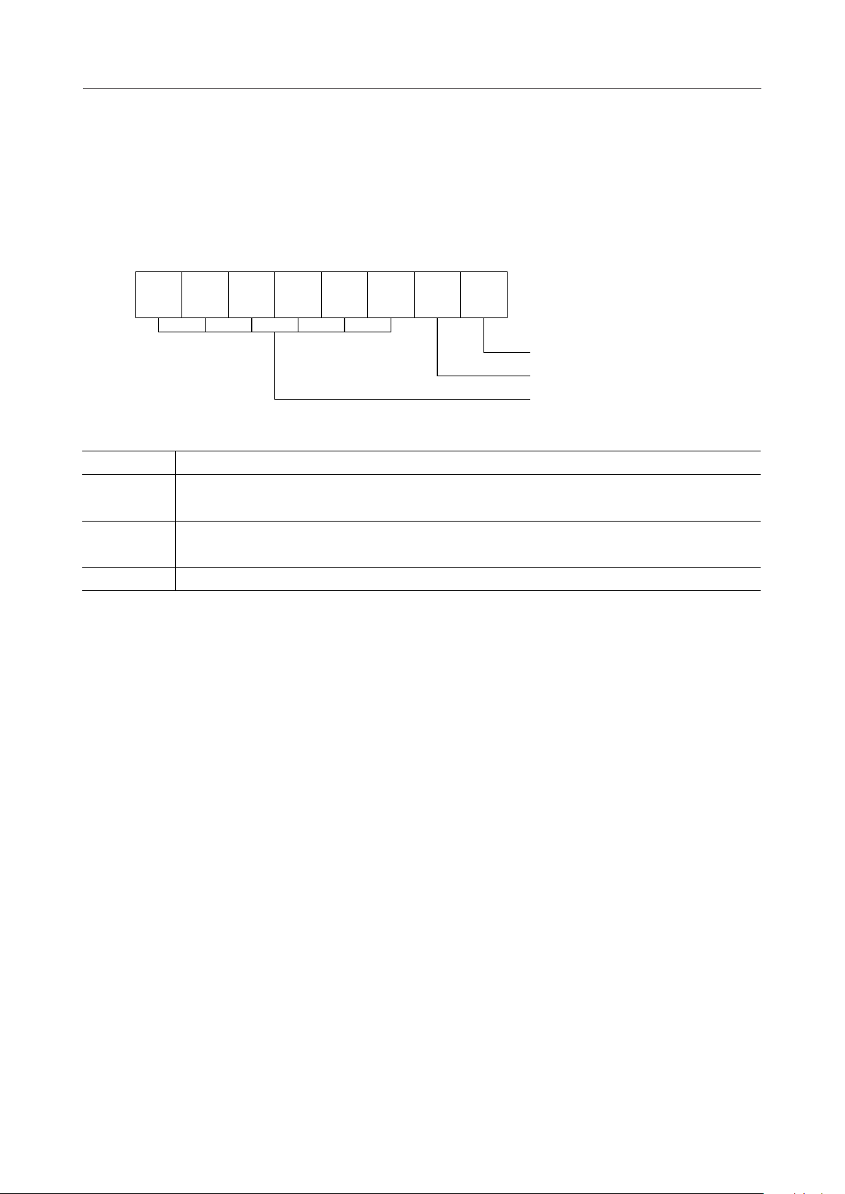
• LSR: Line Status Register (Read Only) (Address = 3h)
The LSR (Line Status Register) indicates various statuses of the MSM9405 that is running. When
the system is reset, all bits of the LSR are set to "0". This register is for read only and cannot be
written.
LSR7LSR6LSR5LSR4LSR3LSR2LSR1LSR
0
TOUT (Timeout = "1")
IR_DET (SIR Pulse detect = "1")
FLV
te number in FIFO
LSR bit
LSR[0]
LSR[1]
Description
TOUT (FIFO Timeout): When time-out occurs in the FIFO during receiving, this bit is set to "1".
When received data is read from the FIFO, TOUT is set to "0".
IR_DET (SIR Pulse detect) : This bit is set to "1" when a pulse having a width of t
upon receiving). It is set to "0" when the CPU reads the LSR.
FLV (FIFO Level): These bits indicate the number of data items in the FIFO with a value of 0 to 32.LSR[2-7]
(SIR pulse width
spw
20/30
Page 21
MSM9405¡ Semiconductor
(
)
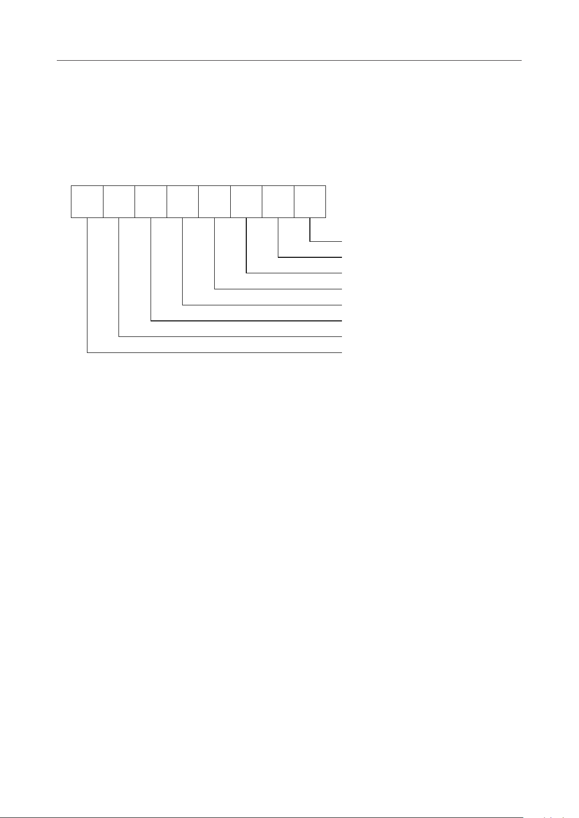
• ICR1: Infrared Control Register 1 (Address = 4h)
The ICR1 (Infrared Control Register 1) is used to set various environment so that the MSM9405
can perform IrDA communication under proper conditions. When the system is reset, all bits
of ICR1 are set to "0".
ICR17ICR16ICR15ICR14ICR13ICR12ICR11ICR1
0
TX_EN ("1": Transmit Enable)
RX_EN ("1": Receive Enable)
S_EOT ("1": Set End Of Transmission)
IR_PLS ("1": Send Interaction Pulse)
FCLR ("1": FIFO Clear)
CRC_INV ("1": Send Inverted CRC Enable)
TCC_EN ("0": TCC off, "1": TCC on)
MS_EN
"1": Automatic mode Select
21/30
Page 22

MSM9405¡ Semiconductor
ICR1 bit
ICR1[0]
ICR1[1]
ICR1[2]
ICR1[3]
ICR1[4]
ICR1[5]
ICR1[6]
ICR1[7]
Description
TX_EN (Transmit Enable): When "1" is written to this bit, the sending mode is selected. When "0" is
written to this bit, sending terminates when data remaining in the FIFO has all been sent. In this
case, the TXE interrupt does not occur.
RX_EN (Receive Enable): When "1" is written to this bit, the receiving mode is selected. When "0" is
written to this bit, the device enters receive end mode.
S_EOT (Set End Of Transmission): This bit is valid in Extended-SIR, MIR, or FIR mode. When "1" is
written to this bit, the data written to the FIFO next time is recognized as the end of frame, and
immediately after it, the data added with CRC and EOF is sent as a frame. After a frame is sent,
this bit is automatically set to "0". To use S_EOT, TFL must be set to the maximum value or TCC
must be unused with TCC_EN = "0". This bit is not used in SIR mode.
IR_PLS (Send Interaction Pulse): This bit is valid in MIR or FIR mode. When "1" is written to
this bit, an approximately 2-ms serial infrared interaction pulse is sent immediately after the frame
being sent. After a frame is sent, this bit is automatically set to "0". This bit is not used in SIR
mode and Extended-SIR mode.
FCLR (FIFO Clear): When "1" is written to this bit, the FIFO (including the TDR and RDR) is made
empty. The FIFO threshold level does not change. The TSR and RSR are not cleared. When the
FIFO is made empty, this bit is automatically set to "0".
CRC_INV (Invert Transmitter CRC): This bit is valid in Extended-SIR, MIR, or FIR mode and is not
used in SIR mode. When "1" is written to this bit, transmission is interrupted if TXE (Transmitter
Empty) occurs. The inverted CRC and EOF are automatically added to the frame that caused TXE,
then the frame is sent. Writing "0" to this bit disables this function.
TCC_EN (TCC Enable): This bit is valid in Extended-SIR, MIR, or FIR mode. When this bit is set to
"1", the TCC is enabled. When TCC_EN is set to "0", the TCC is disabled. To use S_EOT, the TFL
must be set to the maximum value or the TCC must be disabled with TCC_EN = "0".
MS_EN (Mode Select Enable): When "1" is written to this bit, the MSM9405 performs the following
operation depending on the mode. After the operation is completed, this bit is automatically set to
"0".
If the MSM9405 is in FIR mode:
1. The SD pin is set to "H", and the Tx pin to "H".
2. Approximately 300 ns later, the SD pin is set to "L".
3. Approximately 300 ns later, the Tx pin is set to "L".
If the MSM9405 is in SIR, Extended-SIR, or MIR mode:
1. The SD pin is set to "H", and the Tx pin to "L".
2. Approximately 300 ns later, the SD pin is set to "L".
3. The Tx pin is held in the "L" level for approximately 300 ns.
22/30
Page 23
MSM9405¡ Semiconductor
(
)
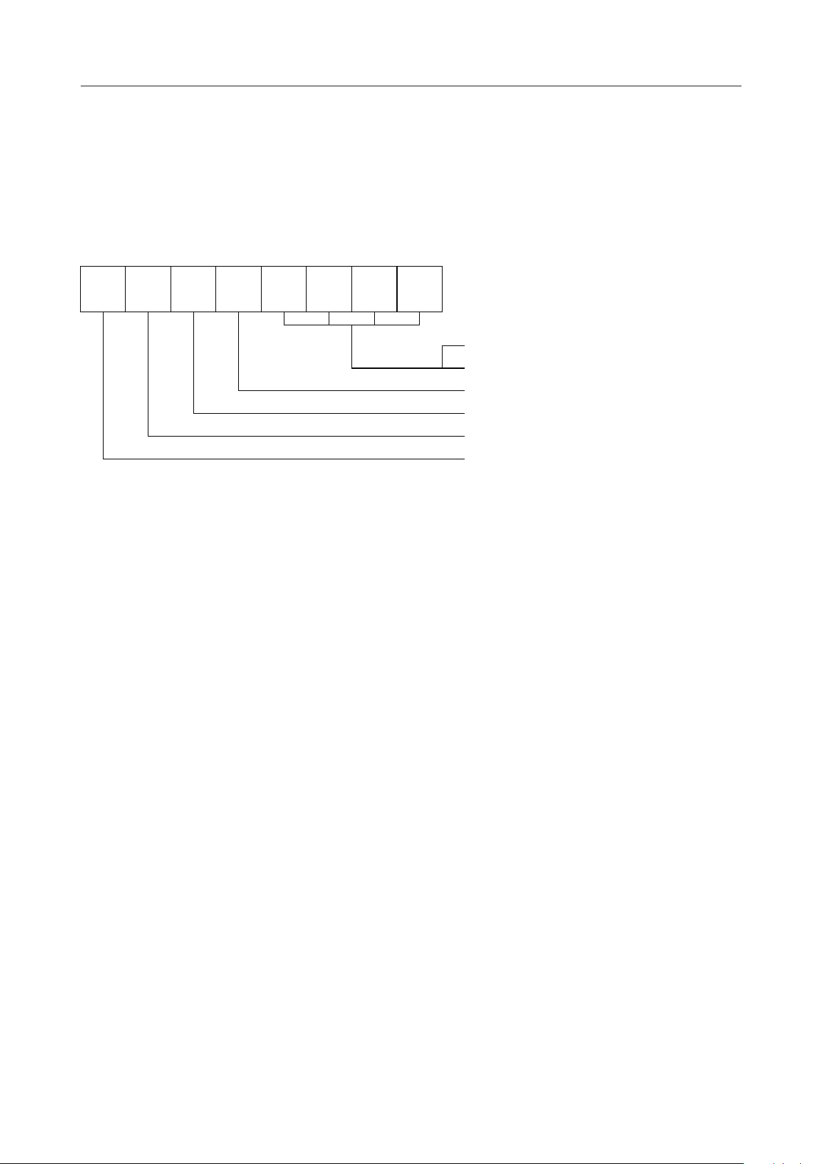
• ICR2: Infrared Control Register 2 (Address = 5h)
The ICR2 (Infrared Control Register 2) is used to set various environment so that the MSM9405
can perform IrDA communication under proper conditions. When the system is reset, all bits
of ICR2 are set to "0".
ICR27ICR26ICR25ICR24ICR23ICR22ICR21ICR2
0
SBF (SIR Beginning Flags)
MBF (MIR Beginning Flags)
RXINV ("1": Signal Invert)
IRIN_SL ("0": Single Input "1": Double Input)
SD_INV ("0": SD Active High "1": SD Active Low)
CTEST
"0": TCC/RST "1": TFL/MDS
23/30
Page 24

MSM9405¡ Semiconductor
IRC2 bit
ICR2[0-3]
Description
These bits work as the SBF when Extended-SIR mode is selected, and as the MBF when the MIR
mode is selected. This function is disabled in SIR mode and FIR mode.
SBF (SIR beginning Flags): These bits determine the number of BOFs to be added during
sending in Extended-SIR mode as shown below.
MBF (MIR Beginning Flags): These bits determine the number of BOFs to be added during
sending in MIR mode as shown below.
Encoding SIR BOFs MIR BOFs
0000 1 2
0001 2 3
0010 3 4
0011 4 5
0100 5 8
0101 7 12
0110 9 16
0111 13 24
1000 17 24
1001 25 24
1010 49 24
1011 49 24
1100
1101
1110
1111
49 24
49 24
49 24
49 24
ICR2[4]
ICR2[5]
ICR2[6]
ICR2[7]
RXINV (IRIN Signal Invert): This bit is used to select active low or active high of the receive signal.
RXINV = "0": Active low
RXINV = "1": Active high
IRIN_SL (IRIN Select): This bit determines how the receive signal input pin is used.
IRIN_SL = "0": Only the input from the IRIN-A pin (2.4 kbps to 4 Mbps) is accepted.
IRIN_SL = "1": An input from IRIN-A or IRIN-B is automatically selected depending on the transfer
rate. (A: 2.4 to 115.2 kbps, B: 0.576 to 4 Mbps)
SD_INV (SD Signal Invert): This bit changes the polarity (active high/low) of the SD pin output on
the MSM9405.
SD_INV = "0": Active high ("H" output during shutdown)
SD_INV = "1": Active low ("L" output during shutdown)
CTEST (Counter Test): Normally this bit is set to "0". When TFL/TCC and MDS/RCC are read after
"1" is written to this bit, the TFL and MDS values can be obtained.
24/30
Page 25
MSM9405¡ Semiconductor
(
)
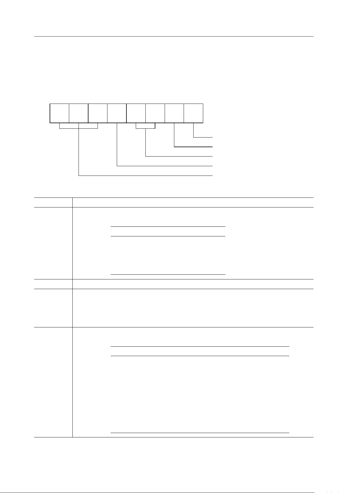
• MSR: Mode Select Register (Address = 6h)
The MSR is used to select various modes of the MSM9405. When the system is reset, each bit
is set to the initial value.
MSR7MSR6MSR5MSR4MSR3MSR2MSR1MSR
0
(IrDA mode Select 0)
IRSL
0
IRSL1 (IrDA mode Select 1)
Not Used
XT_SL ("0": 48 MHz "1": 18.432 MHz)
Data Rate Select
DRS
MSR Bit
IRSL (Infrared Mode Select): These bits are used to select the transfer mode as shown below.
The initial value is set to "00".
IRSL
0 0 SIR
MSR[0-1]
0 1 Extended-SIR
1 0 MIR
1 1 FIR
MSR[2-3] These bits are not used.
XT_SL (Crystal Select): This bit determines the crystal to be used.
The initial value is set to "0".
MSR[4]
XT_SL = "0": 48 MHz crystal is used
XT_SL = "1": 18.432 MHz crystal is used
DRS (Data Rate Select): These bits determine the transfer rate as shown below. The initial value
is set to "001".
Encoding SIR Data Rate MIR Data Rate
000 2400 bps 0.576 Mbps
001 9600 bps 1.152 Mbps 4 Mbps
MSR[5-7]
010 19.2 kbps reserved reserved
011 38.4 kbps
100
101
110
111
Description
1
IRSL
0
mode
FIR Data Rate
reserved
reserved reserved
57.6 kbps
115.2 kbps
reserved
reserved
reserved reserved
reserved reserved
reserved reserved
reserved reserved
25/30
Page 26
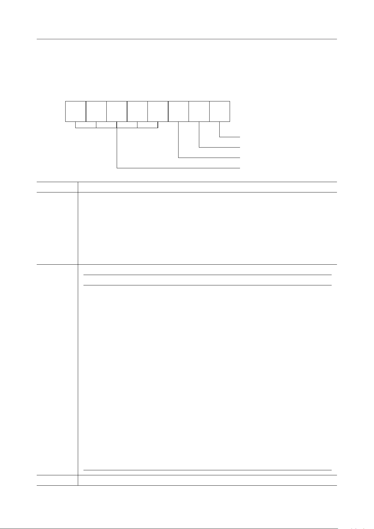
MSM9405¡ Semiconductor
• DSR: DMA Mode Select Register (Address = 7h)
The DSR (DMA Mode Select Register) is used to select the DMA mode for the MSM9405. When
the system is reset, all bits of DSR are set to "0".
DSR7DSR6DSR5DSR4DSR3DSR2DSR1DSR
0
DMA_EN ("1": DMA mode)
DMA_SL0 (DMA Select 0)
DMA_SL
Not Used
(DMA Select 1)
1
DSR Bit
DSR[0]
DSR[1-2]
Description
DMA_EN (DMA Mode Enable): This bit determines whether the DMA is to be used. The initial value
is set to "0".
When "1" is written to this bit, DSR[1-2] (DMA_SL
, DMA_SL1) setting is enabled and the
0
MSM9405 enters the DMA transfer standby mode. (DREQ is asserted when the DREQ assert
condition is met.)
If DMA_EN = "0", DSR[1-2] (DMA_SL
, DMA_SL1) setting is disabled and DMA transfer is not
0
performed. (DREQ is not asserted even if the DREQ assert condition is met.)
DMA_SL (DMA Select): These bits are used to select the method of interfacing with DMAC.
DMA_SL
1
0
FunctionDMA_SL
0 0 DREQ becomes active low and DACK becomes active high.
When the RD signal becomes active while DACK is active,
the DMA read cycle (MemoryÆM9405) is selected. When
the WR signal becomes active while DACK is active, the
DMA write cycle (M9405ÆMemory) is selected. While
DACK is being asserted, address "0" (TDR/RDR) is
accessed regardless of the status of A
to A3.
0
0 1 DREQ becomes active high and DACK becomes active low.
When the WR signal becomes active while DACK is active,
the DMA read cycle (MemoryÆM9405) is selected. When
the RD signal becomes active while DACK is active, the
DMA write cycle (M9405ÆMemory) is selected. While
DACK is being asserted, address "0" (TDR/RDR) is
accessed regardless of the status of A
to A3.
0
1 0 DREQ becomes active low and DACK becomes active high.
DACK is disabled.
1 1 DREQ becomes active high and DACK becomes active low.
DACK is disabled.
These bits are not used.DSR[3-7]
26/30
Page 27
MSM9405¡ Semiconductor
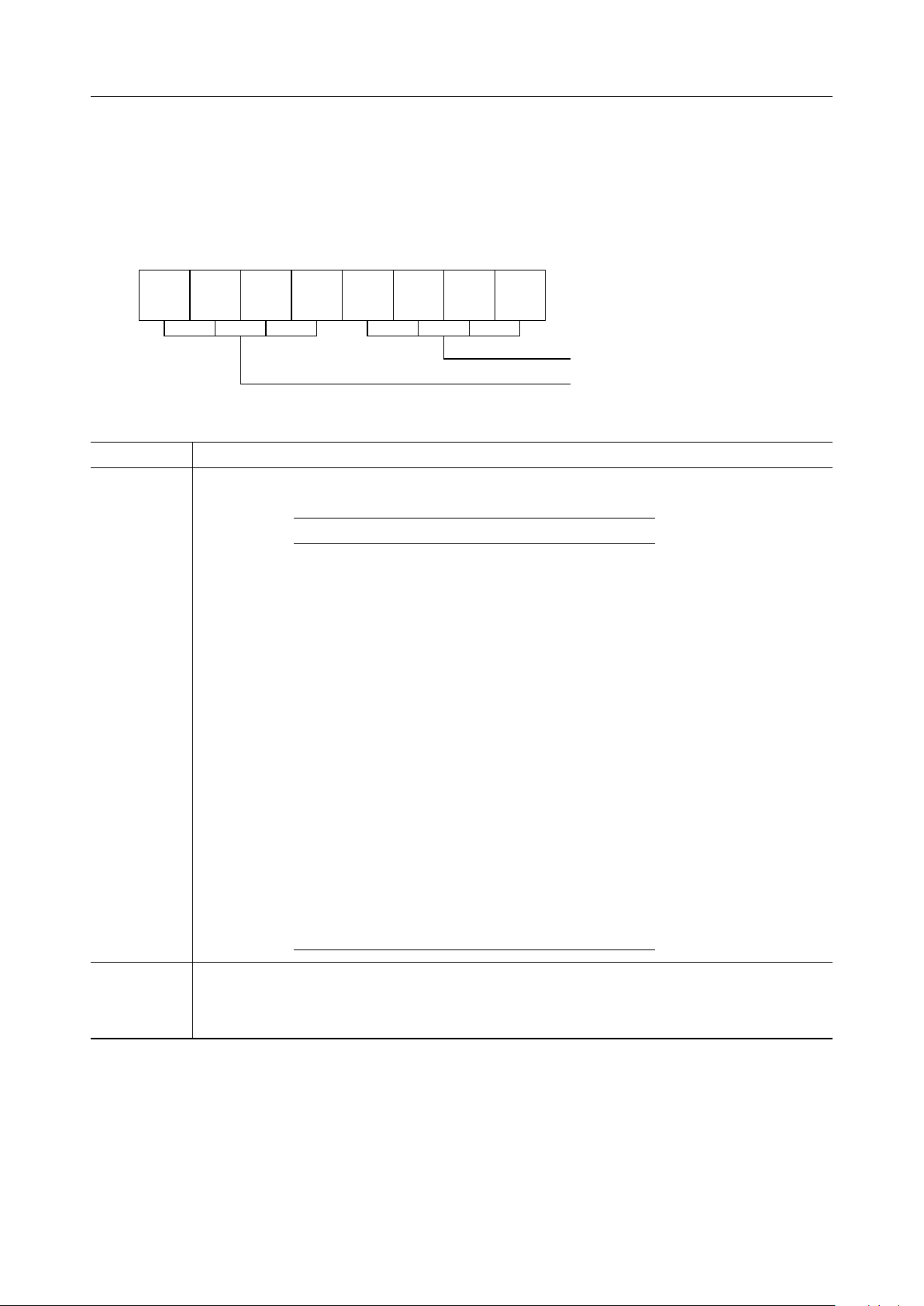
FCR : FIFO Control Register (Address = 8h)
The FCR (FIFO Control Register) is used to set the threshold level of the FIFO to be used by the
MSM9405 upon sending/receiving. The FCR setting is applied to both interrupt and DMA.
When the system is reset, the FCR is set to the initial value.
FCR7FCR6FCR5FCR4FCR3FCR2FCR1FCR
0
TXTH (TX Threshold Select)
RXTH (RX Threshold Select)
FCR bit
FCR[0-3]
Description
TXTH (Transmit Threshold Select): These four bits set the following 16 sending threshold levels.
The initial value is set to "0111".
FCR (0-3) TX Threshold Level (Byte)
0000 01
0001 02
0010 04
0011 06
0100 08
0101 10
0110 12
0111 14
1000 16
1001 18
1010 20
1011 22
1100 24
1101 26
1110 28
1111 30
FCR[4-7]
RXTH (Receive Threshold Select): These four bits set the following 16 receiving threshold levels.
The relationship between the FCR (4-7) value and receiveing threshold level is the same as the
relationship between the FCR (0-3) and sending threshold level. The initial value is set to "0111".
27/30
Page 28

MSM9405¡ Semiconductor
TFL : (Transmitter Frame Length Register
TCC : Transmitter Current-Count Register (Address = 9, Ah)
The TFL (Transmitter Frame Length) and TCC (Transmitter Current-Count Register) are used
to specify the length of the frame to be transferred for sending. The TFL and TCC shares the
same address. Bits 0 to 7 of address 9h and bits 0 to 3 of address Ah (totally 12 bits) are used.
Bit 0 of address 9h is the LSB.
When the TFL/TCC value is read, the CTEST setting is reflected. If CTEST = "0", the TCC
contents can be read. If CTEST = "1", the TFL contents can be read. When the TFL/TCC is
written, the TFL value is rewritten. The TCC cannot be written.
To use the TFL/TCC, write "1" to TCC_EN, and set the frame length in the TFL. The frame length
to be set does not include the CE, FCS, BOF, and EOF. When "1" is written to TX_EN, the TFL
value that has been set as the frame length is loaded to the TCC. When sending is started, the
TCC value is decremented by 1 each time 1 byte is sent. When the TCC value becomes "0", the
end of frame is assumed and the frame is automatically added with the CRC and EOF and sent.
After one frame is sent, the TFL value is loaded again into the TCC when the BOF of the second
frame is sent.
The TFL/TCC initial value is set to 800h.
MDS : Maximum Data Size Register
RST : Receiver Frame Length Stack Register (Address = B, Ch)
The MDS (Maximum Data Size Register) is used to set the maximum data size. The RST
(Receiver Frame Length Stack Register) is used to stack the received frame length. The MDS and
RST share the same address. Bits 0 to 7 of address Bh and bits 0 to 3 of address Ch (totally 12
bits) are used. Bit 0 of address Bh is the LSB.
When the MDS/RST value is read, the CTEST setting is reflected. If CTEST = "0", the RST
contents can be read. If CTEST = "1", the MDS contents can be read. When the MDS/RST is
written, the MDS value is rewritten. The RST cannot be written.
To use the MDS, set the maximum data size in the MDS in advance. The frame length to be set
does not include the CE, FCS, BOF, and EOF in the Extended-SIR, MIR, and FIR modes.
(However, it does include them in the SIR mode.) When receiving is started, the internal counter
value is incremented by 1 each time one byte is received. If the internal counter value exceeds
the MDS value during receiving, MLE occurs. The MDS initial value is set to 800h.
When a frame is fully received and all the data in the received frame is taken out of the FIFO,
the received frame length counted by the internal counter is stacked in the RST. This value is
stored untill the next frame is fully received. The value stacked in the RST is maintained even
if MSM9405 sending/receiving is switched. The RST initial value is set to 0h.
TEST : Test Register (Address = Fh)
This register is used for testing.
28/30
Page 29
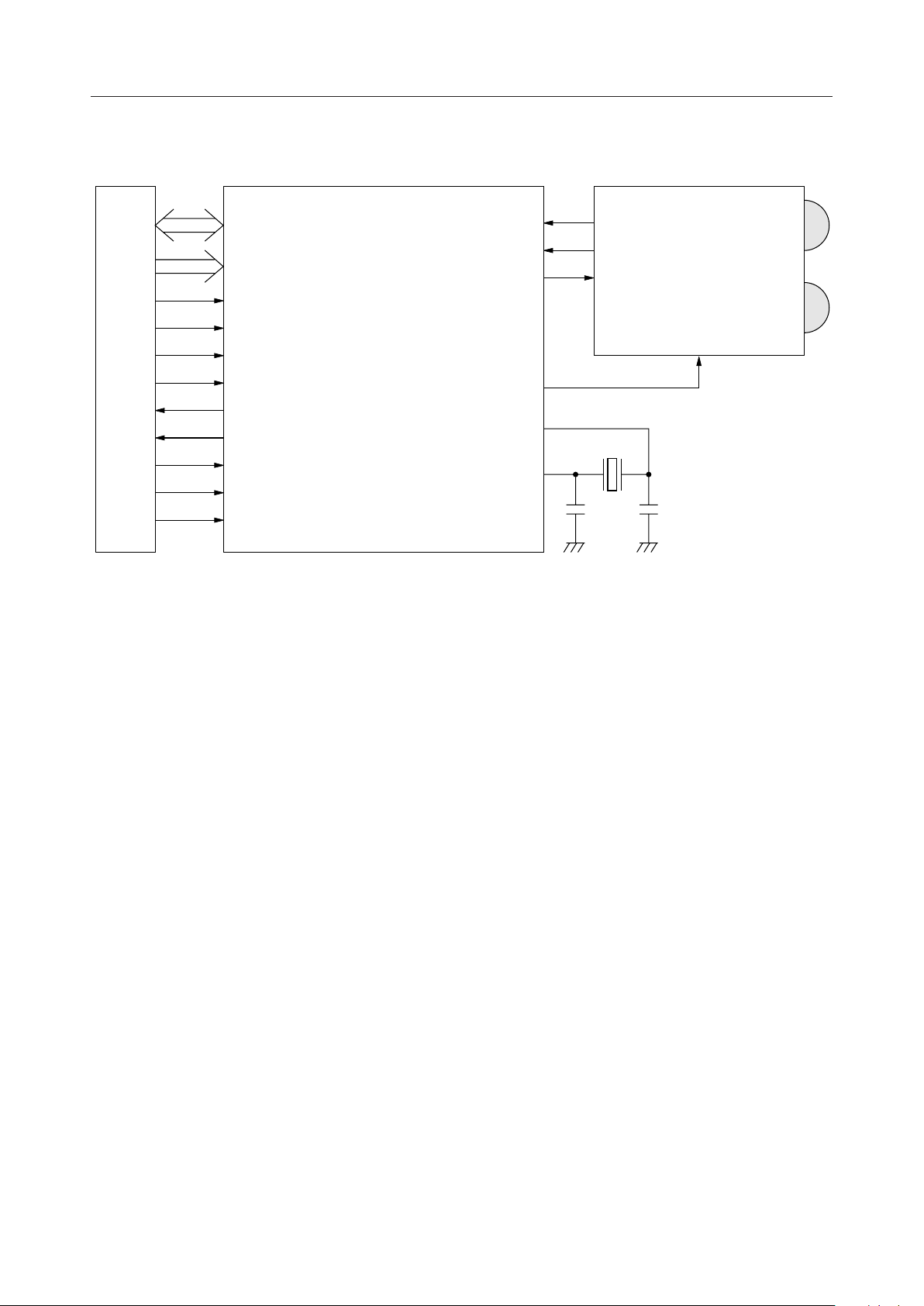
APPLICATION CIRCUIT
MSM9405¡ Semiconductor
Microcontroller
D0-D
A
0-A3
CS
RD
WR
TC
INTR
DREQ
DACK
RESET
PWDN
7
IRIN-B
RXD-AIRIN-A
(RXD-B)
TXDIROUT
Infrared
Transceiver
Module
SD
MSM9405
SD
XIN
XOUT
29/30
Page 30
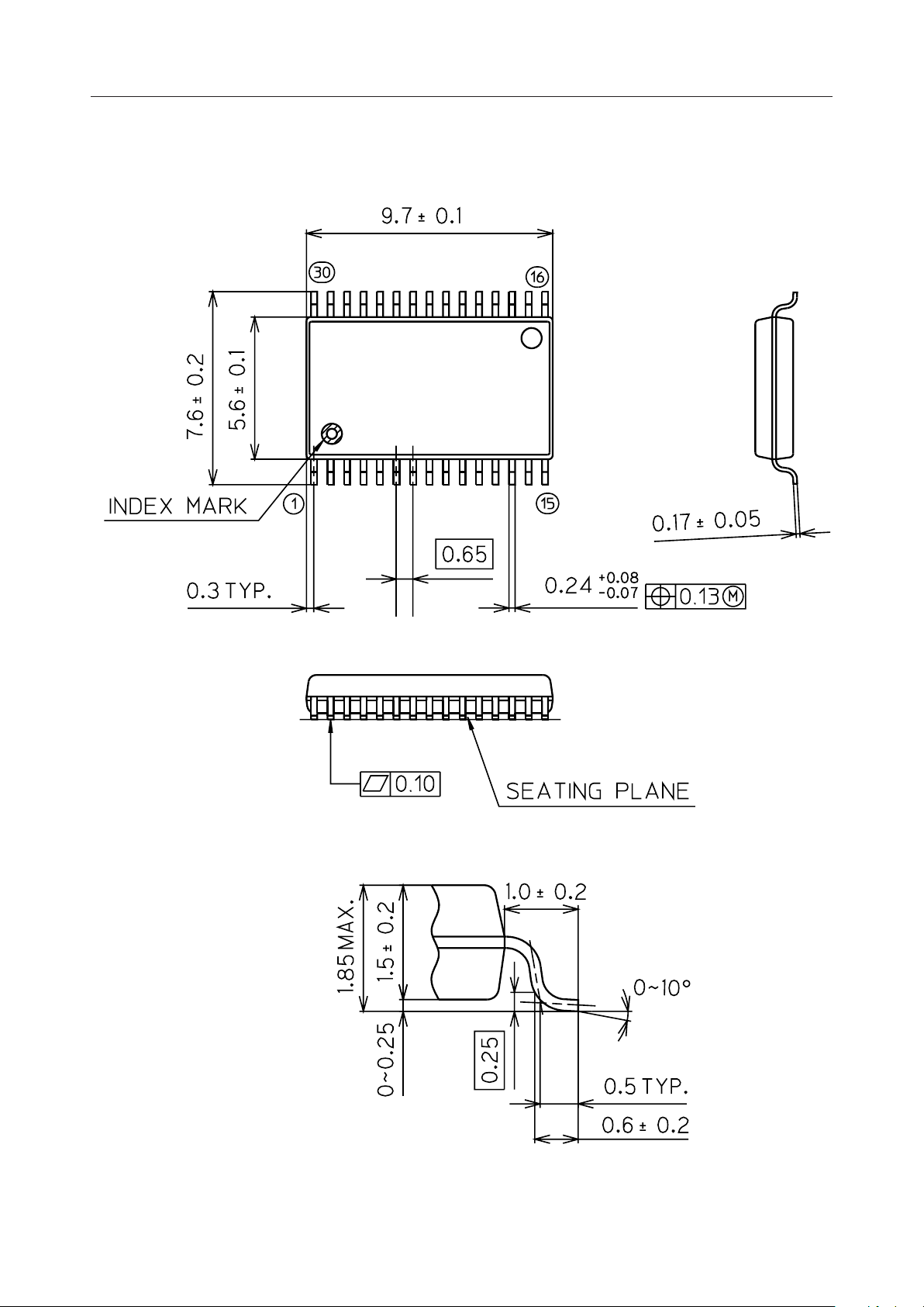
PACKAGE OUTLINES AND DIMENSIONS
MSM9405¡ Semiconductor
(Unit : mm)
Mirror finish
30-Pin Plastic SSOP
30/30
 Loading...