

Page 1

E2D0019-39-92
Preliminary
¡ Semiconductor
This version: Sep. 1999
Previous version: May. 1997
MSM98P05¡ Semiconductor
MSM98P05
Voice Synthesis IC with Built-in 2-Mbit OTP ROM
GENERAL DESCRIPTION
The MSM98P05 is a PCM-based voice synthesis IC with built-in 2-Mbit OTP (One Time PROM).
This IC employs OKI nonlinear PCM algorithm and straight PCM algorithm for playback and
contains a current mode 10-bit D/A converter and a low-pass filter.
External control can be made easily by the built-in edit ROM that can form sentences by linking
phrases. With OKI Voice Analyzing/Editing Tool, the built-in edit ROM can be set up and also
the built-in ROM data can be created and evaluated easily.
With the stand-alone mode/microcontroller interface mode switching pin, the MSM98P05 can
support various applications.
The products with build-in OTP are suited to applications to be produced in small quantities in
a wide variety or in short delivery time. Demand like these, that is, production in small quantities
in a wide variety and delivery with an early deadline is what the MSM9800 family of products
with built-in mask ROM cannot meet.
FEATURES
• 8-bit OKI nonlinear PCM algorithm and 8-bit straight PCM algorithm
• Built-in edit ROM
• Random playback function
• Sampling frequency : 4.0 kHz/5.3 kHz/6.4 kHz/8.0 kHz/10.6 kHz/12.8 kHz/
16.0 kHz
Note: If RC oscillation is selected, 10.6 kHz, 12.8 kHz, and
16.0 kHz cannot be selected.
• Maximum number of phrases : 63 (Microcontroller interface mode)
56 (Stand-alone mode)
• Built-in current mode 10-bit D/A converter
• Built-in low-pass filter (LPF)
• Standby function
• RC oscillation (256 kHz)/ceramic oscillation (4.096 MHz) selectable
• Package options:
20-pin plastic DIP (DIP20-P-300-2.54-W1) (Product name : MSM98P05RS)
24-pin plastic SOP (SOP24-P-430-1.27-K) (Product name : MSM98P05GS-K)
1/13
Page 2
2/13
MSM98P05¡ Semiconductor
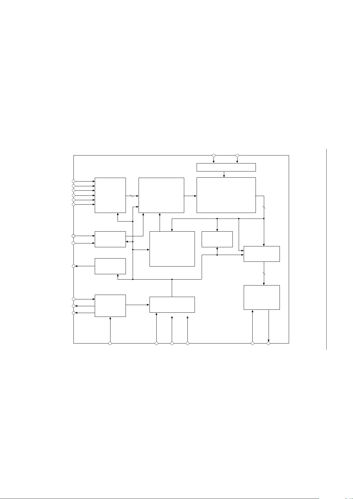
STAND-ALONE MODE (CPU/STD: "L" level)
BLOCK DIAGRAM
2-Mbit OTP ROM
(Including 11 Kbits of
Edit ROM & Address ROM)
18-Bit
Multiplexer
Address &
Switching
Controller
6
PCM
Synthesizer
10
8
10-Bit
DAC
&
LPF
AOUT
DATA
Controller
18-Bit
Address Counter
Timing Controller
GNDV
DD
RESET
Random
Circuit
I/O
Interface
OSC
XT/RC
XT/CR
A2
A1
A0
SW2
SW1
SW0
RND
BUSY
OSC1
OSC2
OSC3/TEST
CPU/STD
V
REF
Program Circuit
V
PP
PGM
Page 3
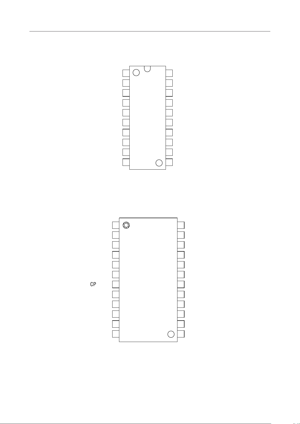
PIN CONFIGURATION (TOP VIEW)
MSM98P05¡ Semiconductor
V
PP
A0
A1
A2
RESET
XT/CR
BUSY
GND
V
REF
1
2
3
4
5
6
7
8
9
10 11AOUT V
20
PGM
19
SW2
18
SW1
17
SW0
16
RND
15
CPU/STD
14
OSC3/TEST
13
OSC2
12
OSC1
DD
20-Pin Plastic DIP
Note: Applies to MSM98P05RS
V
1
DD
NC
NC
RND
2
3
4
5
6
7
8
9
10
11
12
OSC1
OSC2
OSC3/TEST
CPU/STD XT/CR
PGM
SW0
SW1
SW2
24
23
22
21
20
19
18
17
16
15
14
13
NC: No connection
24-Pin Plastic SOP
AOUT
V
REF
GND
NC
BUSY
NC
RESET
V
PP
A2
A1
A0
Note: Applies to MSM98P05GS-K
3/13
Page 4
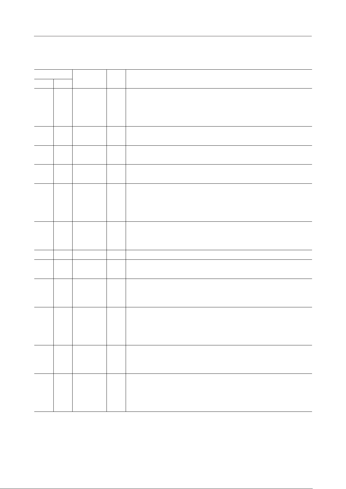
PIN DESCRIPTIONS
MSM98P05¡ Semiconductor
DIP
5
7
6
15
9
10
8
11
12
13
14
16
Pin
SOP
17
20
18
7
23
24
22
1
2
3
5
8
Symbol Type Description
The IC enters the standby state if this pin is set to "L" level. At this time,
oscillation stops and AOUT drives a current of 0mA and becomes GND level,
RESET I
then the IC returns to the initial state. Apply a "L" pulse during power-on.
This pin has an internal pull-up resistor.
Outputs "L" level while voice is being played back.
BUSY O
In "H" level when power is turned ON.
XT/RC switching pin. Set to "H" level if ceramic oscillation is used. Set to "L"
XT/CR I
level if RC oscillation is used.
Microcontroller interface/stand-alone mode switching pin. Set to "L" level if
CPU/STD I
the IC is used in stand-alone mode.
Volume setting pin. If this pin is set to GND level, the maximum amplitude is
V
REF
I
This pin is internally connected to a pull-down resistor of approx. 10 kW
delivered. If this pin is set to V
level, the minimum amplitude is delivered.
DD
during IC operation.
Voice output pin.
AOUT O
The voice signals are output as current changes. A logic "L" is output from
this pin in standby state.
GND —
Ground pin.
Power supply pin. Insert a bypass capacitor of 0.1 mF or more between V
V
DD
—
and GND pins.
Ceramic oscillator connection pin when ceramic oscillation is selected.
OSC1 I
RC connection pin when RC oscillation is selected.
Input from this pin if external clock is used.
Ceramic oscillator connection pin when ceramic oscillation is selected.
RC connection pin when RC oscillation is selected.
OSC2 O
Leave this pin open if external clock is used.
Outputs "L" level in standby state.
Leave this pin open when ceramic oscillation is used.
OSC3/TEST O
RC connection pin when RC oscillation is selected.
Outputs "H" level in standby state when RC oscillation is selected.
Random playback starts if RND pin is set to "L" level.
Fetches addresses from random address generation circuit in the IC at the
RND I
falling edge of RND. Set to "H" level when the random playback function is
not used. This pin has internal pull-up resistor.
DD
4/13
Page 5

MSM98P05¡ Semiconductor
DIP
17-19
2-4
1
20
Pin
SOP
10-12
13-15
16
9
Symbol Type Description
Phrase input pins corresponding to playback sound.
SW0 - SW2 I
A0 - A2 I
V
PP
PGM I
If input changes, SW0 to SW2 pins fetch addresses after 16 ms and start voice
synthesis. Each of these pins has internal pull-down resistor.
Phrase input pins corresponding to playback sound.
Logic input to A0 pin becomes invalid if the random playback function is used.
Power supply pin for writing to the built-in OTP. This pin should be set to "H"
—
level or be open during playback.
Interface pin for writing to the built-in OTP. This pin should be set to "L"
level or be open during playback.
5/13
Page 6
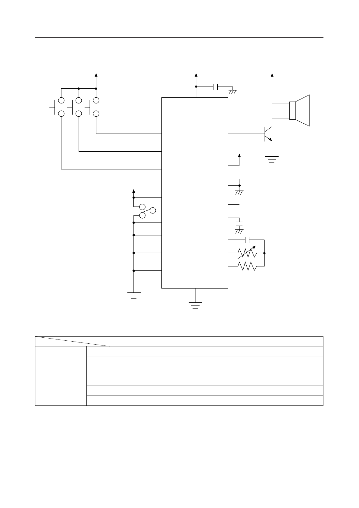
APPLICATION CIRCUITS
S3 S2 S1
MSM98P05¡ Semiconductor
V
DD
S4
SW0
SW1
SW2
RND
A0
A1
A2
XT/CR
CPU/STD
GND
AOUT
V
PP
PGM
V
REF
BUSY
RESET
OSC3
OSC2
OSC1
S4="L"
S4="H"
Address [HEX]SW0SW1SW2A0A1A2
100000S1
010000S2
001000S3
100100S1
010100S2
001100S3
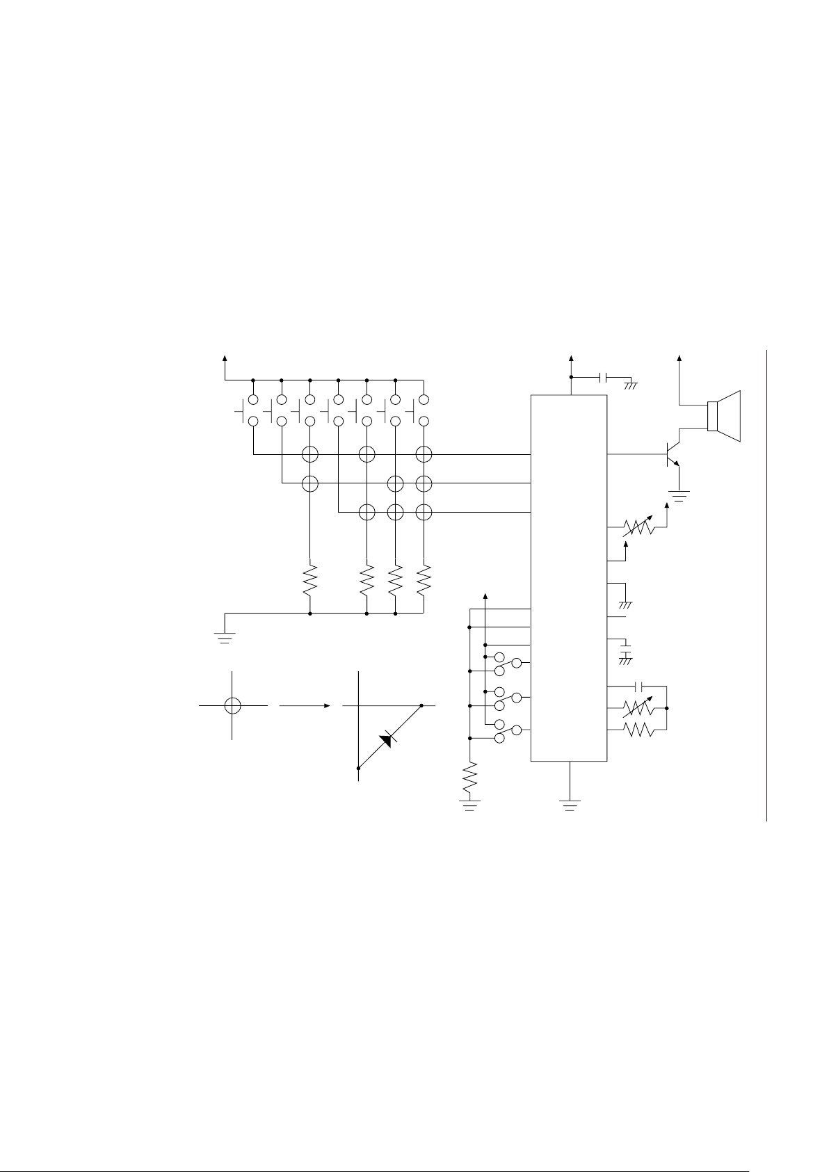
Application Circuit for Playing Six Phrases Using Four Switches
01
02
04
09
0A
0C
6/13
Page 7
7/13
MSM98P05¡ Semiconductor
1234567
SW0
SW1
SW2
AOUT
V
DD
XT/CR
CPU/STD
RND
A0
A1
A2
GND
OSC3
OSC2
OSC1
V
REF
V
PP
PGM
BUSY
RESET
Application Circuit Using Switches
Page 8
8/13
MSM98P05¡ Semiconductor
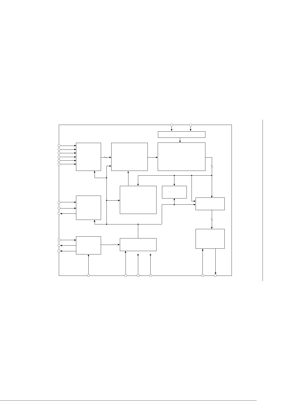
MICROCONTROLLER INTERFACE MODE (CPU/STD: "H" level)
BLOCK DIAGRAM
2-Mbit OTP ROM
(Including 11 Kbits of
Edit ROM & Address ROM)
18-Bit
Multiplexer
Address
Controller
6
PCM
Synthesizer
10
8
10-Bit
DAC
&
LPF
AOUT
DATA
Controller
18-Bit
Address Counter
Timing Controller
GNDV
DD
RESET
I/O
Interface
OSC
XT/RC
XT/CR
I5
I4
I3
I2
I1
I0
ST
NAR
OSC1
OSC2
OSC3/TEST
CPU/STD
V
REF
Program Circuit
V
PP
PGM
Page 9
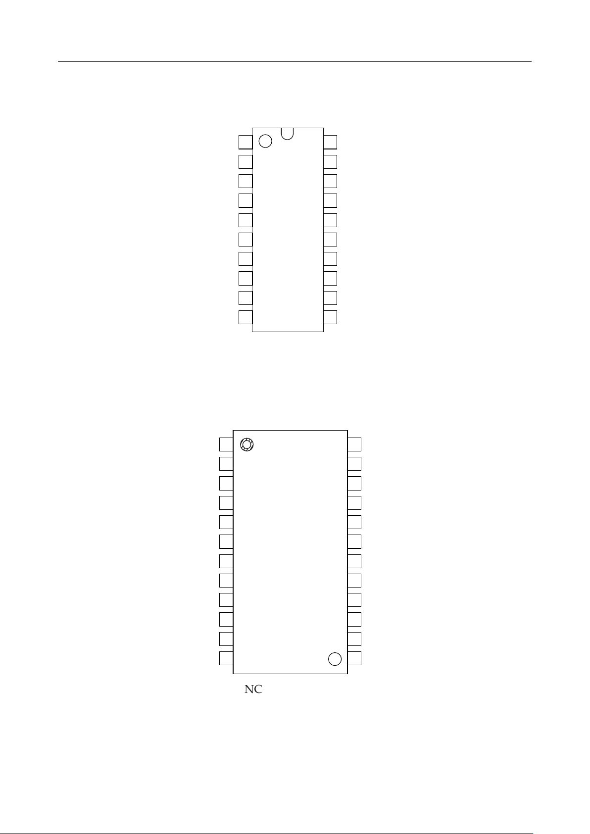
PIN CONFIGURATION (TOP VIEW)
MSM98P05¡ Semiconductor
V
PP
I3
I4
I5
RESET
XT/CR
NAR
GND
V
REF
1
2
3
4
5
6
7
8
9
20
PGM
19
I2
18
I1
17
I0
16
ST
15
CPU/STD
14
OSC3/TEST
13
OSC2
12
OSC1
10 11AOUT V
20-Pin Plastic DIP
Note: Applies to MSM98P05RS
DD
V
DD
OSC1
OSC2
NC
OSC3/TEST
NC
CPU/STD
ST
PGM
I0
I1
I2
1
2
3
4
5
6
7
8
9
10
11
12
NC: No connection
24-Pin Plastic SOP
24
23
22
21
20
19
18
17
16
15
14
13
AOUT
V
REF
GND
NC
NAR
NC
XT/CR
RESET
V
PP
I5
I4
I3
Note: Applies to MSM98P05GS-K
9/13
Page 10
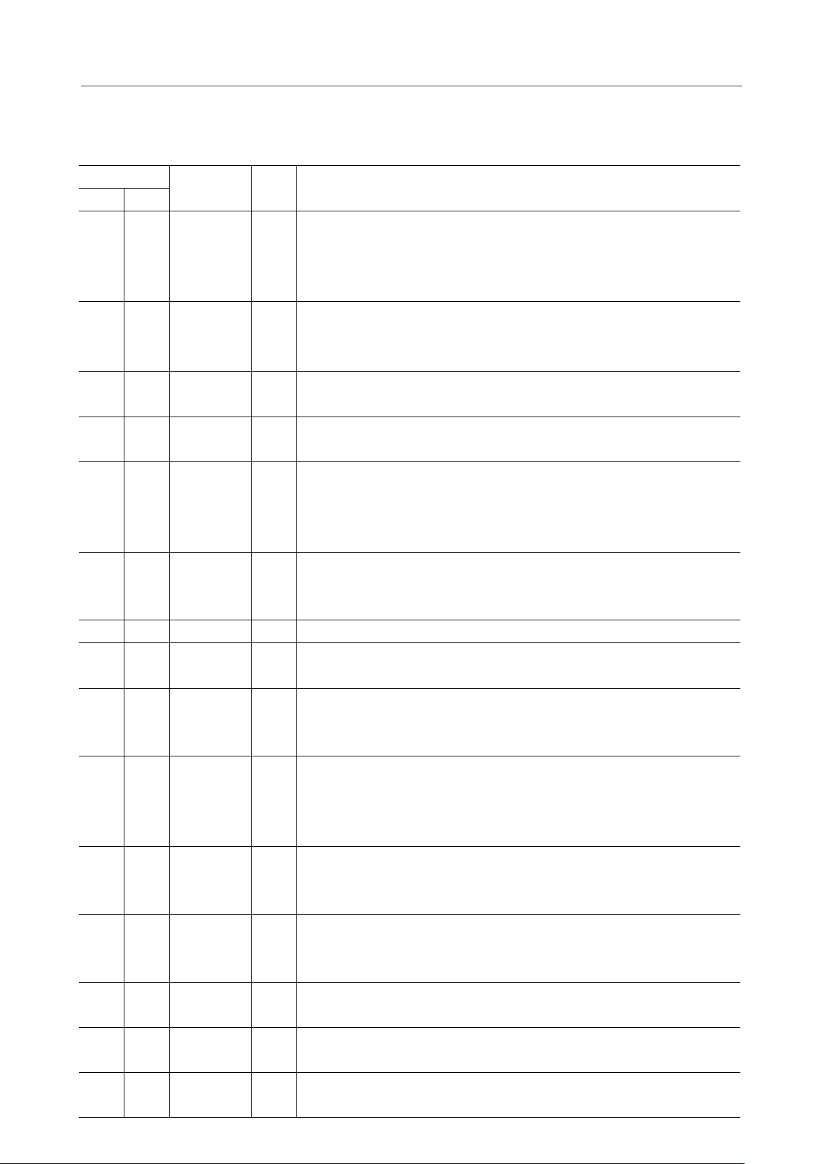
PIN DESCRIPTIONS
MSM98P05¡ Semiconductor
DIP
5
7
6
15
9
10
8
11
12
13
14
16
17-19
2-4
1
20
Pin
SOP
17
20
18
7
23
24
22
1
2
3
5
8
10-15
16
9
Symbol Type Description
The IC enters the standby state if this pin is set to "L" level. At this time,
oscillation stops and AOUT drives a current of 0mA and becomes GND level,
RESET I
then the IC returns to the initial state. If the power cannot be applied within 1ms,
apply an "L" pulse during power-on. This pin has an internal pull-up resistor.
Signal output pin that indicates whether the register in the address controller
NAR O
to latch the 10-15 addresses (see Block Diagram) is idle. NAR at "H" level
indicates that the LATCH is empty and ST input is enabled.
XT/RC switching pin. Set to "H" level if ceramic oscillation is used. Set to "L"
XT/CR I
level if RC oscillation is used.
Microcontroller interface/stand-alone mode switching pin. Set to "H" level if
CPU/STD I
the IC is used in microcontroller interface mode.
Volume setting pin. If this pin is set to GND level, the maximum amplitude is
V
REF
I
This pin is internally connected to a pull-down resistor of approx. 10 kW
delivered. If this pin is set to V
level, the minimum amplitude is delivered.
DD
during IC operation.
Voice output pin.
AOUT O
The voice signals are output as current changes. A logic "L" is output from
this pin in standby state.
GND —
Ground pin.
Power supply pin. Insert a bypass capacitor of 0.1 mF or more between this
V
DD
—
pin and the GND pin.
Ceramic oscillator connection pin when ceramic oscillation is selected.
OSC1 I
RC connection pin when RC oscillation is selected.
Input from this pin if external clock is used.
Ceramic oscillator connection pin when ceramic oscillation is selected.
RC connection pin when RC oscillation is selected.
OSC2 O
Leave this pin open if external clock is used.
Outputs "L" level in standby state.
Leave this pin open when ceramic oscillation is used.
OSC3/TEST O
RC connection pin when RC oscillation is selected.
Outputs "H" level in standby state when RC oscillation is selected.
Voice synthesis starts at fall of ST, and addresses I0 to I5 are fetched at rise
ST I
of ST. Input ST when NAR, the status signal, is at "H" level.
This pin has internal pull-up resistor.
Phrase input pins corresponding to vocalized sound.
I0 - I5 I
Power supply pin for writing to the built-in OTP. This pin should be set to "H"
V
PP
—
level or be open.
Interface pin for writing to the built-in OTP. This pin should be set to "L" level
PGM I
or be open.
10/13
Page 11
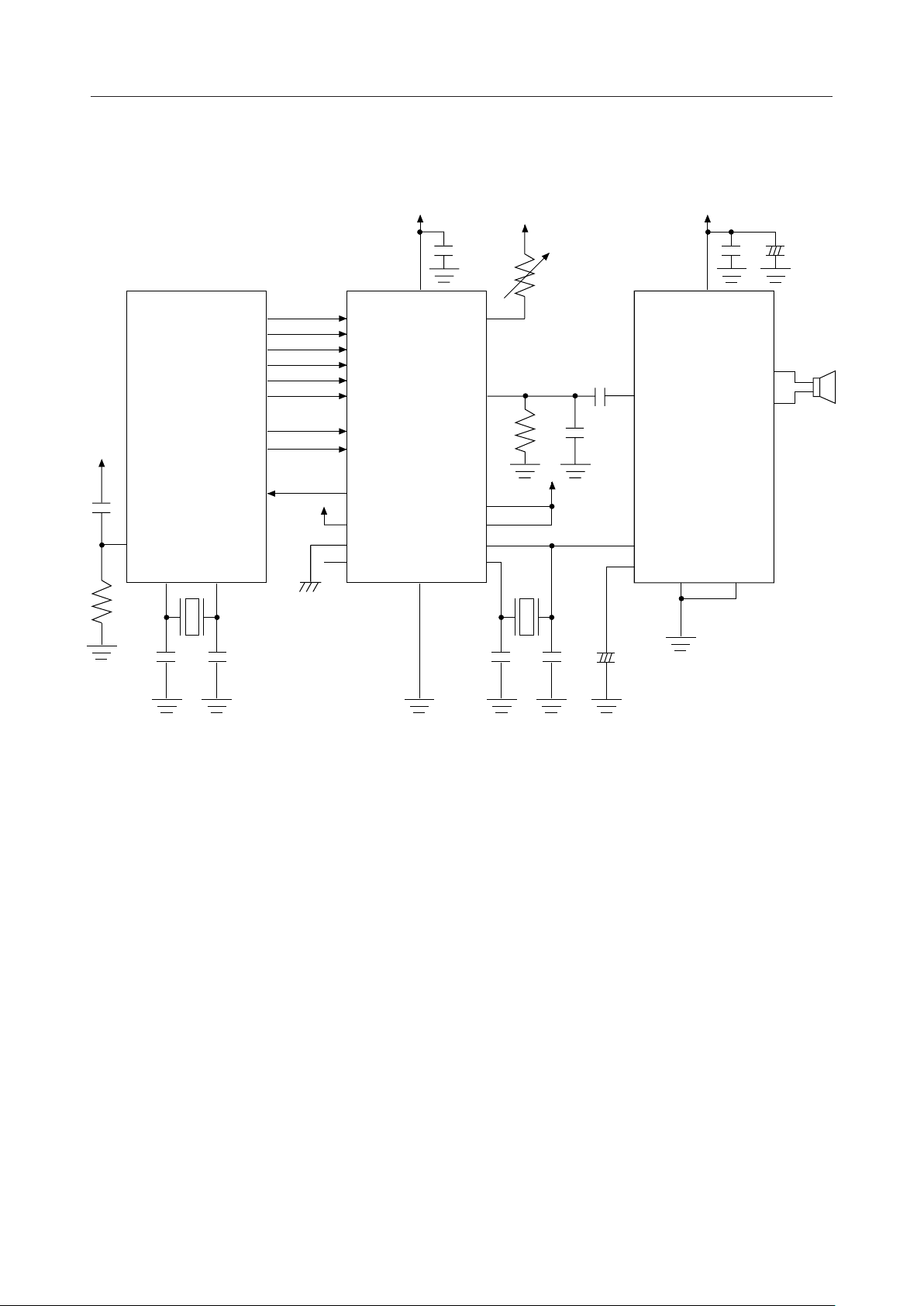
APPLICATION CIRCUIT
MSM98P05¡ Semiconductor
+
–
RESET
P1.5
P1.4
P1.3
P1.2
P1.1
P1.0 I0
P2.2
P2.1
MSM83C154 (MCU)
P3.0 NAR
XTAL2XTAL1
I5
I4
I3
I2
I1
ST
RESET
V
PP
PGM
OSC3
V
DD
MSM98P05
CPU/STD
GND
V
REF
AOUT
XT/CR
OSC2
OSC1
V
CC
SP
A
IN
STBY
VR
GND
+
–
SP
MSC1157 (Speaker AMP)
SEL
Application Circuit when Used as Microcontroller Interface
11/13
Page 12
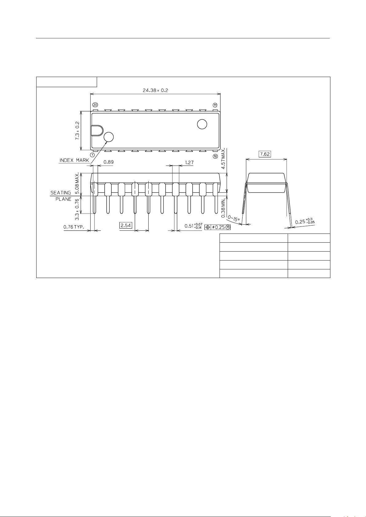
PACKAGE DIMENSIONS
DIP20-P-300-2.54-W1
MSM98P05¡ Semiconductor
(Unit : mm)
Package material
Lead frame material
Pin treatment
Solder plate thickness
Package weight (g)
Epoxy resin
42 alloy
Solder plating
5 mm or more
1.50 TYP.
12/13
Page 13
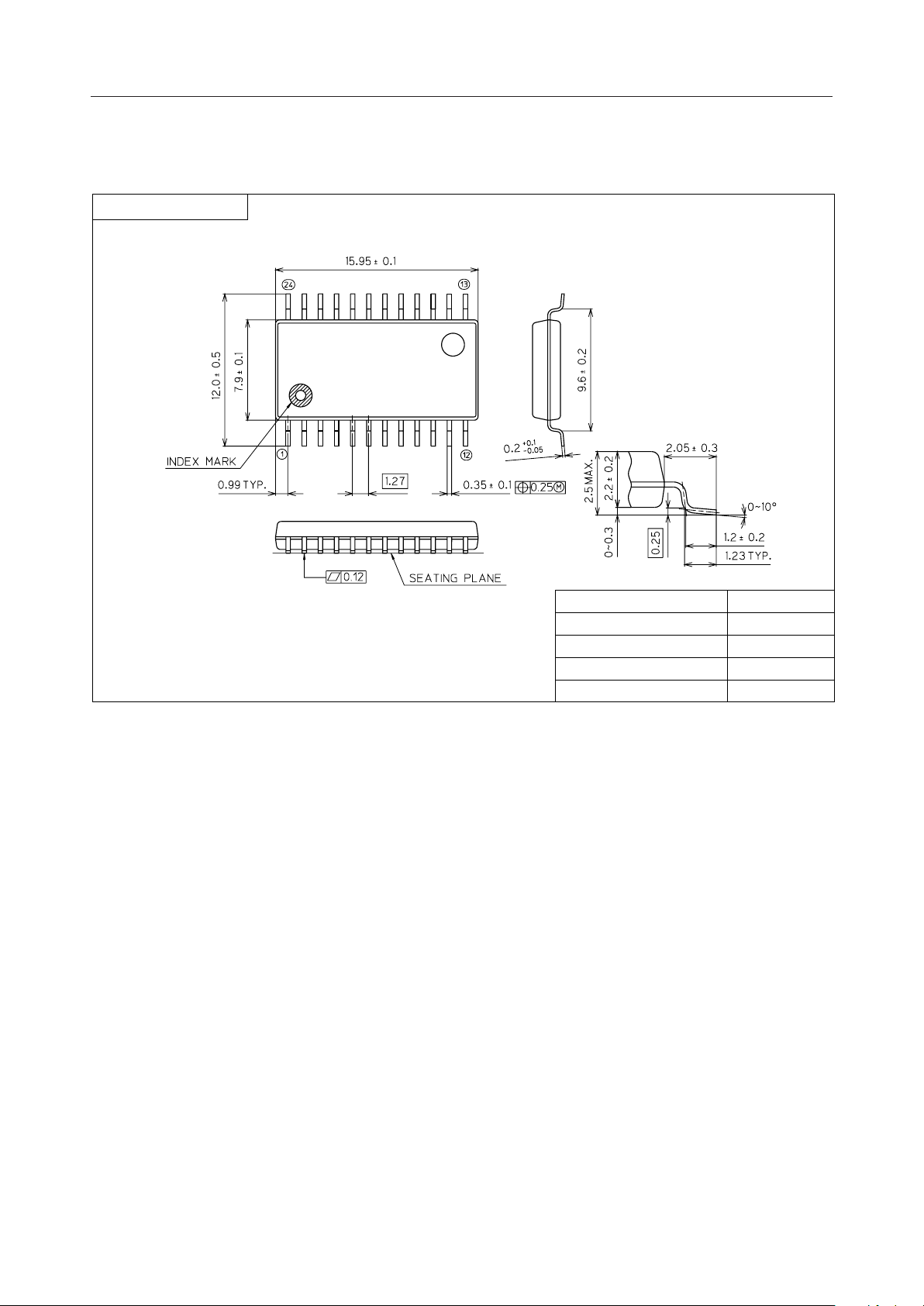
SOP24-P-430-1.27-K
Mirror finish
MSM98P05¡ Semiconductor
(Unit : mm)
Package material
Lead frame material
Pin treatment
Solder plate thickness
Package weight (g)
Epoxy resin
42 alloy
Solder plating
5 mm or more
0.58 TYP.
Notes for Mounting the Surface Mount Type Package
The SOP, QFP, TSOP, SOJ, QFJ (PLCC), SHP and BGA are surface mount type packages, which
are very susceptible to heat in reflow mounting and humidity absorbed in storage.
Therefore, before you perform reflow mounting, contact Oki’s responsible sales person for the
product name, package name, pin number, package code and desired mounting conditions
(reflow method, temperature and times).
13/13
Page 14

E2Y0002-29-62
NOTICE
1. The information contained herein can change without notice owing to product and/or
technical improvements. Before using the product, please make sure that the information
being referred to is up-to-date.
2. The outline of action and examples for application circuits described herein have been
chosen as an explanation for the standard action and performance of the product. When
planning to use the product, please ensure that the external conditions are reflected in the
actual circuit, assembly, and program designs.
3. When designing your product, please use our product below the specified maximum
ratings and within the specified operating ranges including, but not limited to, operating
voltage, power dissipation, and operating temperature.
4. Oki assumes no responsibility or liability whatsoever for any failure or unusual or
unexpected operation resulting from misuse, neglect, improper installation, repair, alteration
or accident, improper handling, or unusual physical or electrical stress including, but not
limited to, exposure to parameters beyond the specified maximum ratings or operation
outside the specified operating range.
5. Neither indemnity against nor license of a third party’s industrial and intellectual property
right, etc. is granted by us in connection with the use of the product and/or the information
and drawings contained herein. No responsibility is assumed by us for any infringement
of a third party’s right which may result from the use thereof.
6. The products listed in this document are intended for use in general electronics equipment
for commercial applications (e.g., office automation, communication equipment,
measurement equipment, consumer electronics, etc.). These products are not authorized
for use in any system or application that requires special or enhanced quality and reliability
characteristics nor in any system or application where the failure of such system or
application may result in the loss or damage of property, or death or injury to humans.
Such applications include, but are not limited to, traffic and automotive equipment, safety
devices, aerospace equipment, nuclear power control, medical equipment, and life-support
systems.
7. Certain products in this document may need government approval before they can be
exported to particular countries. The purchaser assumes the responsibility of determining
the legality of export of these products and will take appropriate and necessary steps at their
own expense for these.
8. No part of the contents contained herein may be reprinted or reproduced without our prior
permission.
9. MS-DOS is a registered trademark of Microsoft Corporation.
Copyright 1999 Oki Electric Industry Co., Ltd.
Printed in Japan
 Loading...