

Page 1

E2C0044-19-96
¡ Semiconductor
¡ Semiconductor
This version: Sep. 1999
Previous version: Aug. 1999
MSM9223
MSM9223
27-Bit Duplex/Triplex VFD Controller/Driver with Digital Dimming, ADC and Keyscan
GENERAL DESCRIPTION
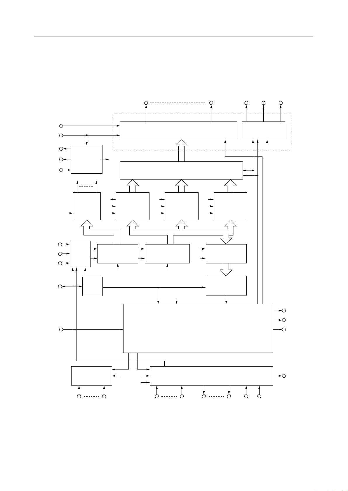
The MSM9223 is a full CMOS controller/driver for Duplex or Triplex vacuum fluorescent
display tube. It conststs of 27-segment driver outputs and 3-grid pre-driver outputs, so that it
can drive directly up to 81-segment VFD.
MSM9223 features a digital dimming function, a 6-ch ADC, a 5 ¥ 5 keyscan circuit and an encoder
type switch interface.
MSM9223 provides an interface with a microcontroller only by three signal lines: DATA I/O,
CLOCK and CS.
FEATURES
• Supply voltage (VDD) : 8 to 18.5V (Built-in 5V regulator for logic)
• Duplex/Triplex selectable
• Applicable VFD tube : 2 Grids ¥ 27 Anodes VFD tube
: 3 Grids ¥ 27 Anodes VFD tube
• 27-segment driver outputs : IOH=–5mA at VOH=VDD–0.8V (SEG1 to 19)
IOH=–10mA at VOH=VDD–0.8V (SEG20 to 27)
• 3-grid pre-driver outputs : IOL=10mA at VOL=2V
• Built-in digital dimming circuit (10-bit resolution)
• Built-in 6-ch A/D converter
• Built-in 5 ¥ 5 keyscan circuit
• Interface circuit for an encoder type rotary switch
• Built-in oscillation circuit (external R and C)
• Built-in Power-On-Reset circuit
• Package:
64-pin plastic QFP (QFP64-P-1420-1.00-BK) Product name: MSM9223GS-BK
1/24
Page 2
¡ Semiconductor
BLOCK DIAGRAM
MSM9223
GRID2 GRID3GRID1SEG27SEG1
D-GND
V
V
(5V)
VREG
(5V)
L-GND
CS
CLOCK
DATA I/O
OSCO
DD
CC
POR
5V
Regulator
&
Power On
Reset
0H 7H
Mode Select
in1-3
Control
OSC
POR
1H
0H
POR
Out1-27
Segment Latch
1
in1-27
Out1-3
3bit Shift Register
POR
27 Segment Driver
Out1-27
81 to 27 Segment Control
in1-27 in1-27in1-27
2H
0H
POR
Out1-27
Segment Latch
2
in1-27
Out1-27
27bit Shift Register
POR
POR
4H
POR
3H
Segment Latch
0H
POR
Dimming Latch
Out1-10
10bit Digital
Dimming
3 Grid pre Driver
Out1-27
3
in1-27
in1-10
Timing Generator
6ch, 8bit
A/D Converter
7H
5H
6H
5 ¥ 5 Key Scan and Encoder Switch Interface
CH1 CH6 COL1 COL5 ROW1 ROW5 A1 B1
DIM OUT
SYNC OUT1
SYNC OUT2DUP/TRI
INT
2/24
Page 3
¡ Semiconductor
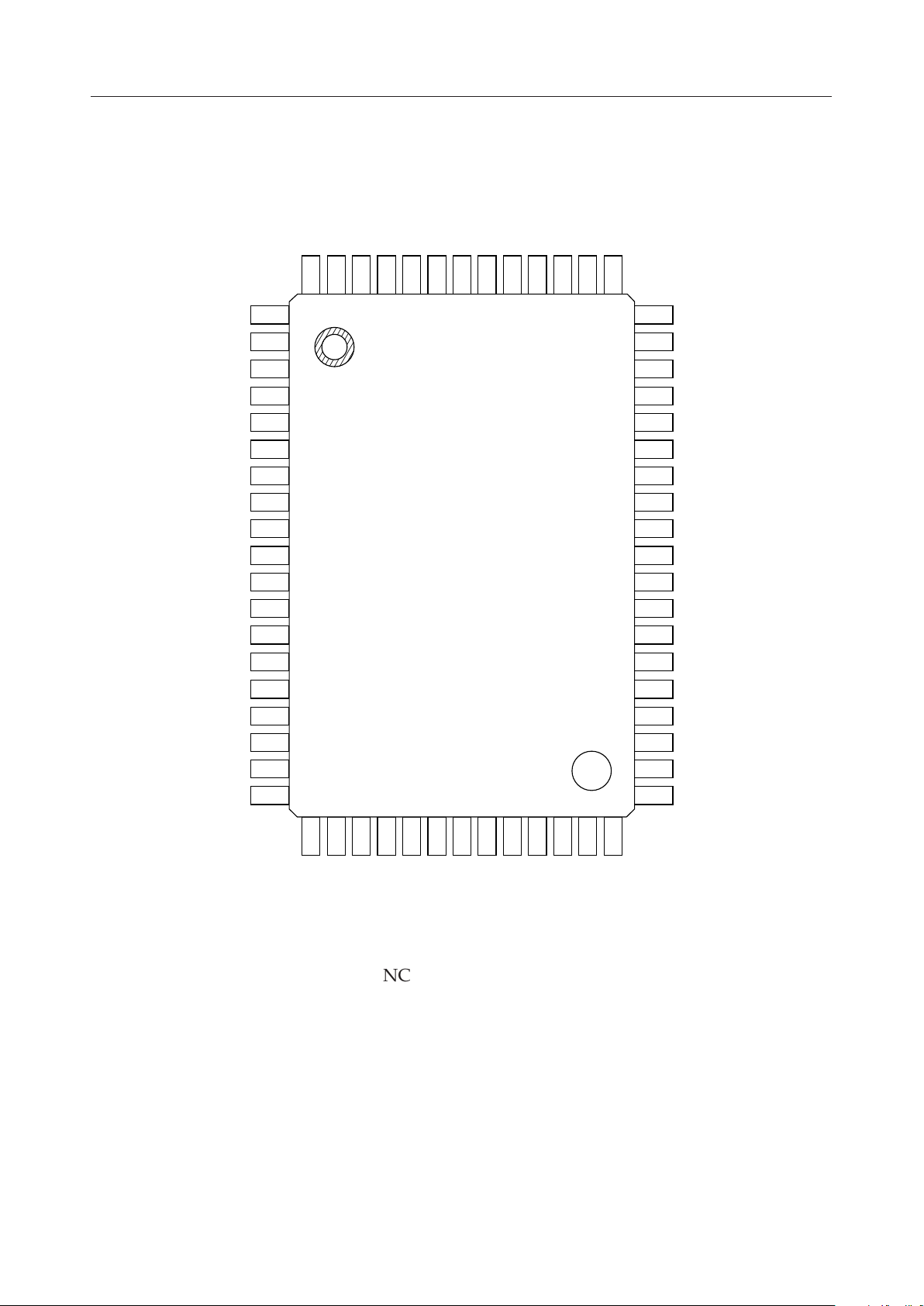
PIN CONFIGURATION (TOP VIEW)
MSM9223
V
DD
SEG25
SEG26
SEG27
GRID1
GRID2
GRID3
D-GND
ROW1
ROW2
ROW3
ROW4
ROW5
COL1
COL2
COL3
COL4
COL5
NC
10
11
12
13
14
15
16
17
18
19
SEG18
SEG21
SEG22
SEG23
SEG24
64
63
62
61
1
2
3
4
5
6
7
8
9
SEG19
SEG20
60
59
58
SEG16
SEG17
57
56
SEG15
SEG14
55
54
SEG13
SEG12
53
52
51
50
49
48
47
46
45
44
43
42
41
40
39
38
37
36
35
34
33
V
DD
SEG11
SEG10
SEG9
SEG8
SEG7
SEG6
SEG5
SEG4
SEG3
SEG2
SEG1
CH6
CH5
CH4
CH3
CH2
CH1
VREG
20A121B122
INT
23
24
25
26
27
28
CC
V
OSCO
DUP/TRI
L-GND
CLOCK
DATA I/O
NC: No connection
64-pin Plastic QFP
29
30
CS
SYNC OUT2
31
32
DIM OUT
SYNC OUT1
3/24
Page 4

¡ Semiconductor
PIN DESCRIPTIONS
MSM9223
Pin Type Description
1, 51 —
8—
26 —
24 OV
33 OV
40 to 50,
52 to 59
Symbol
V
DD
D-GND
L-GND
CC
REG
SEG1 to 19
Power supply pins.
Pin1 and pin51 should be connected externally.
D-GND is ground pin for the VFD driver circuit. L-GND is ground pin for the
logic circuit. Pins 8 and 26 should be connected externally.
5V output pin for internal logic portion and external logic circuit.
Reference voltage (5V) output pin for A/D converter.
Segment (anode) signal output pins for a VFD tube.
These pins can be directly connected to the VFD tube. External circuit is not required.
O
IOH£–5 mA
Segment (anode) signal output pins for a VFD tube.
60 to 64,
These pins can be directly connected to the VFD tube. External circuit is not required.
2 to 4
SEG20 to 27
O
IOH£–10 mA
Inverted Grid signal output pins.
5, 6, 7 O
GRID1 to 3
For pre-driver, the external circuit is requiend.
IOL£10 mA
29 I
CS
Chip Select input pin.
Data input/output operation is valid when this pin is set at a High level.
28 I
27 I/O
CLOCK
DATA I/O
Serial clock input pin.
Data is input and/or output through the DATA I/O pin at the rising edge of the serial clock.
Serial data input/output pin.
Data is input to / comes out from the shift register at the rising edge of the serial clock.
Interrupt signal output to microcontroller. When any key of key matrix is pressed
22 O
INT
or released, key scanning is started. After the completion of the one cycle, this pin
goes to high level and keeps the high level until keyscan stop mode is selected.
Duplex/Triplex operation select input pin.
23 I
DUP/TRI
Duplex (1/2 duty) operation is selected when this pin is set at a V
Triplex (1/3 duty) operation is selected when this pin is set at a GND level.
34 to 39 ICH1 to 6
Analog voltage input pin for the 8-bit A/D converter.
Input pin for the encoder type rotary switch. Each input has chattering
20, 21
A1, B1
O
absorption function of 620ns typical.
CC
level.
14 to 18 I
9 to 13 O
COL1 to 5
ROW1 to 5
Return inputs from the key matrix.
These pins are active low. When key matrix are in the inactive sate, these
pins are at high level through the internal pull-up resistors. All the inputs do
not have the cahttering absorption function for the keyscans.
Key switch scanning outputs.
Normally low level is output through these pin. When any switch of key matrix
is depressed or released, key scanning is started and is continued until
keyscan stop mode is selected. When keyscan stop mode is selected, all
outputs of ROW1 to 5 go back to low level.
4/24
Page 5
¡ Semiconductor
MSM9223
Pin Type Description
32 O
Symbol
DIM OUT
Dimming pulse output.
Connect this pin to the slave side DIM IN pin.
Synchronous signal input.
30, 31 O
SYNC OUT 1, 2
Connect these pins to the SYNC IN1 and SYNC IN2 pins
of a slave side.
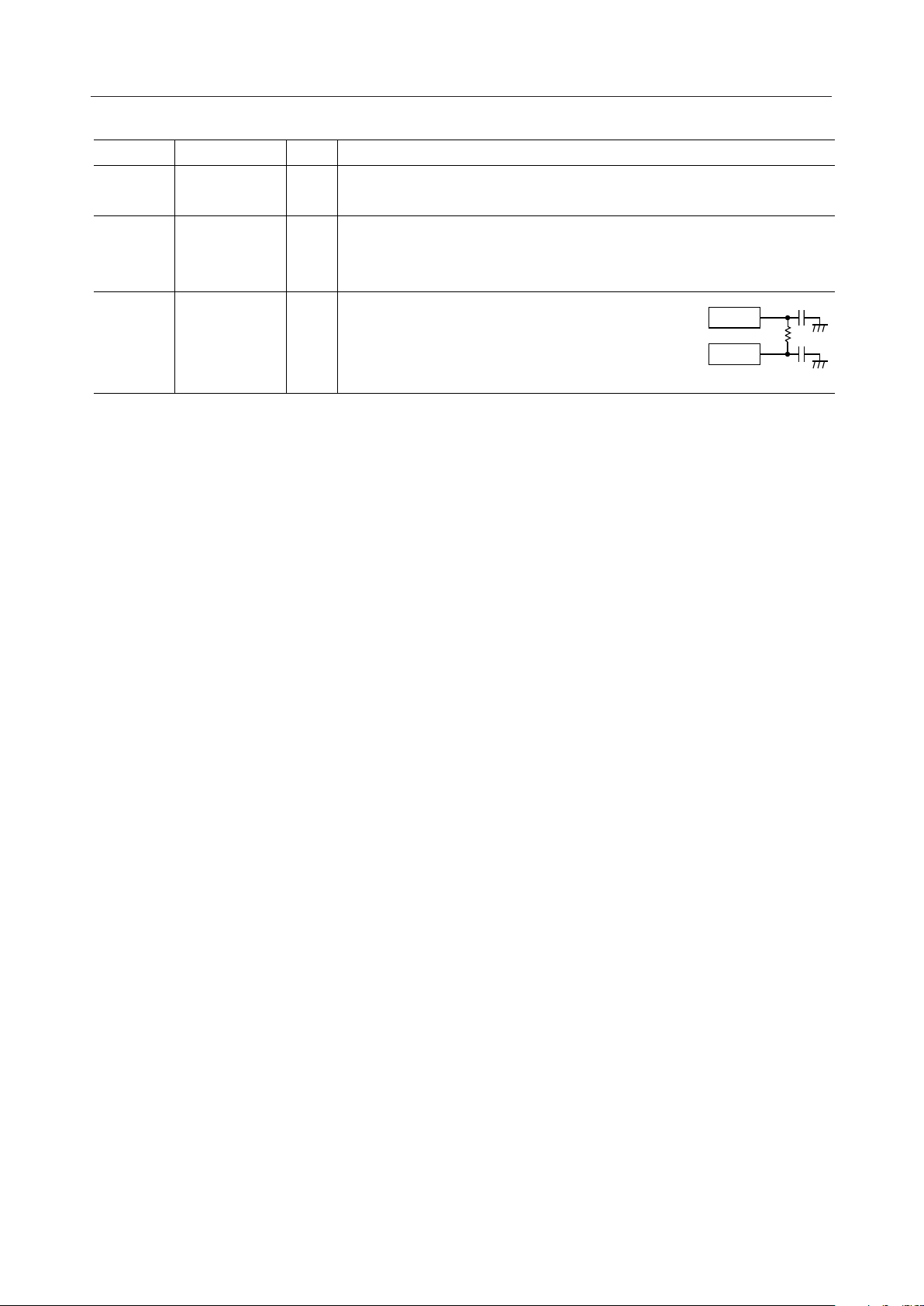
RC oscillator connecting pins.
25 I/O
OSC0
Connect a resistor (R2) between the V
and OSC0 pins,
CC
and a capacitor (C2) between the OSC0 pin and the GND,
and a capacitor (C3) between the V
and the GND. C3 is for VCC stabilization.
CC
V
CC
OSC0
C
3
R
2
C
2
5/24
Page 6
¡ Semiconductor
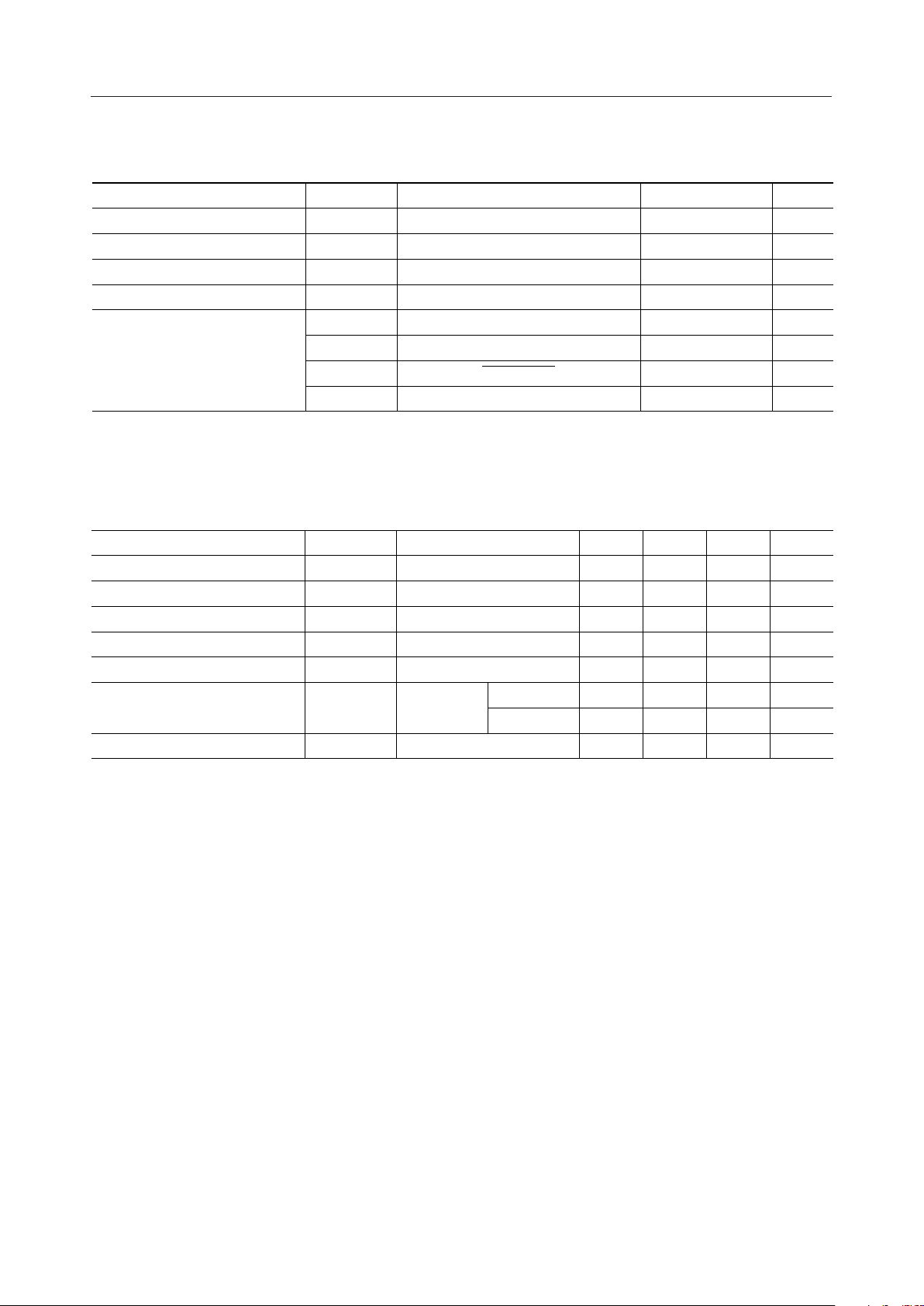
ABSOLUTE MAXIMUM RATINGS
Parameter Symbol Condition Rating Unit
V
DD
V
IN
Ta = 85°C mWPower Dissipation
SEG1 to 19 mA
SEG20 to 27 mA
GRID1 to 3 mA
Output Current
T
P
STG
I
O1
I
O2
I
O3
I
O4
D
DIM OUT, SYNC OUT1, SYNC OUT2 mA
RECOMMENDED OPERATING CONDITIONS
MSM9223
—VSupply Voltage
—VInput Voltage
—°CStorage Temperature
–0.3 to +20
–0.3 to +6.0
590
–55 to +150
–10.0 to +2.0
–20.0 to +2.0
–7.0 to +20.0
–2.0 to +2.0
Parameter Symbol
Driver Supply Voltage
High Level Input Voltage
Low Level Input Voltage
Clock Frequency
Oscillation Frequency
Frame Frequency
Operating Temperature
V
V
V
f
f
OSC
f
T
FR
DD
IH
IL
C
OP
Condition Min. Typ. Max. Unit
— 8.0 13.0 18.5 V
All inputs except OSC0 3.8 — 5.5 V
All inputs except OSC0 0.0 — 0.8 V
— — — 1.0 MHz
R2 = 10kW±5%, C2 = 27pF±5%
R2 = 10kW±5%
= 27pF±5%
C
2
1/3 Duty 211 269 325 Hz
1/2 Duty 317 403 488 Hz
2.6 3.3 4.0 MHz
— –40 — +85 °C
6/24
Page 7
¡ Semiconductor
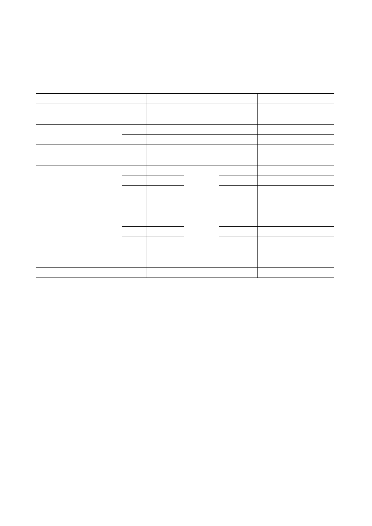
ELECTRICAL CHARACTERISTICS
DC Characteristics
MSM9223
V
V
I
IH1
I
IH2
I
IL1
I
IL2
OH1
OH2
OH3
OH4
OL1
OL2
OL3
OL4
IH
IL
DD
L
Applied pin
*1)
*1)
*2)
*3)
*2)
*3)
SEG1 to 19
SEG20 to 27
GRID1 to 3
*4)
SEG1 to 19
SEG20 to 27
GRID1 to 3
*5)
V
DD
V
CC
V
V
C3=0.01mF±10%, IO=0 to –10mA
Parameter Symbol
High Level Input Voltage
Low Level Input Voltage
High Level Input Current
Low Level Input Current
V
V
High Level Output Voltage
V
V
V
V
Low Level Output Voltage
V
V
Supply Current f
Supply Voltage for Logic
(Ta=–40 to +85°C, V
=8.0 to 18.5V)
DD
Condition Min. Max. Unit
— 3.8 5.5 V
— 0.0 0.8 V
=3.8V –5.0 +5.0 mA
V
IH
VIH=3.8V –100 –5.0 mA
=0.0V –5.0 +5.0 mA
V
IL
=0.0V –300 –70 mA
V
IL
–0.8 V
V
DD
–0.8 V
V
DD
–0.8 V
V
DD
4.0 5.5 V
4.5 5.5 V
— 2.0 V
— 2.0 V
— 2.0 V
— 0.8 V
—10mAI
=9.5V
DD
=9.5V
DD
=3.3MHz, no load
OSC
I
=–5mA
OH1
=–10mA
I
OH2
=–5mA
I
OH3
=–200mA
I
OH4
Output Open
I
=500mA
OL1
=500mA
I
OL2
=10mA
I
OL3
=300mA
I
OL4
4.5 5.5 VV
DD
DD
DD
V
V
V
*1) CS, CLOCK, DATA I/O DUP/TRI, A1, B1, COL1 to 5
*2) CS, CLOCK, DATA I/O DUP/TRI, A1, B1
*3) COL1 to 5
*4) DATA I/O, INT, DIM OUT, SYNC OUT1, SYNC OUT2
*5) DATA I/O, INT, DIM OUT, SYNC OUT1, SYNC OUT2, ROW1 to 5
7/24
Page 8
¡ Semiconductor
MSM9223
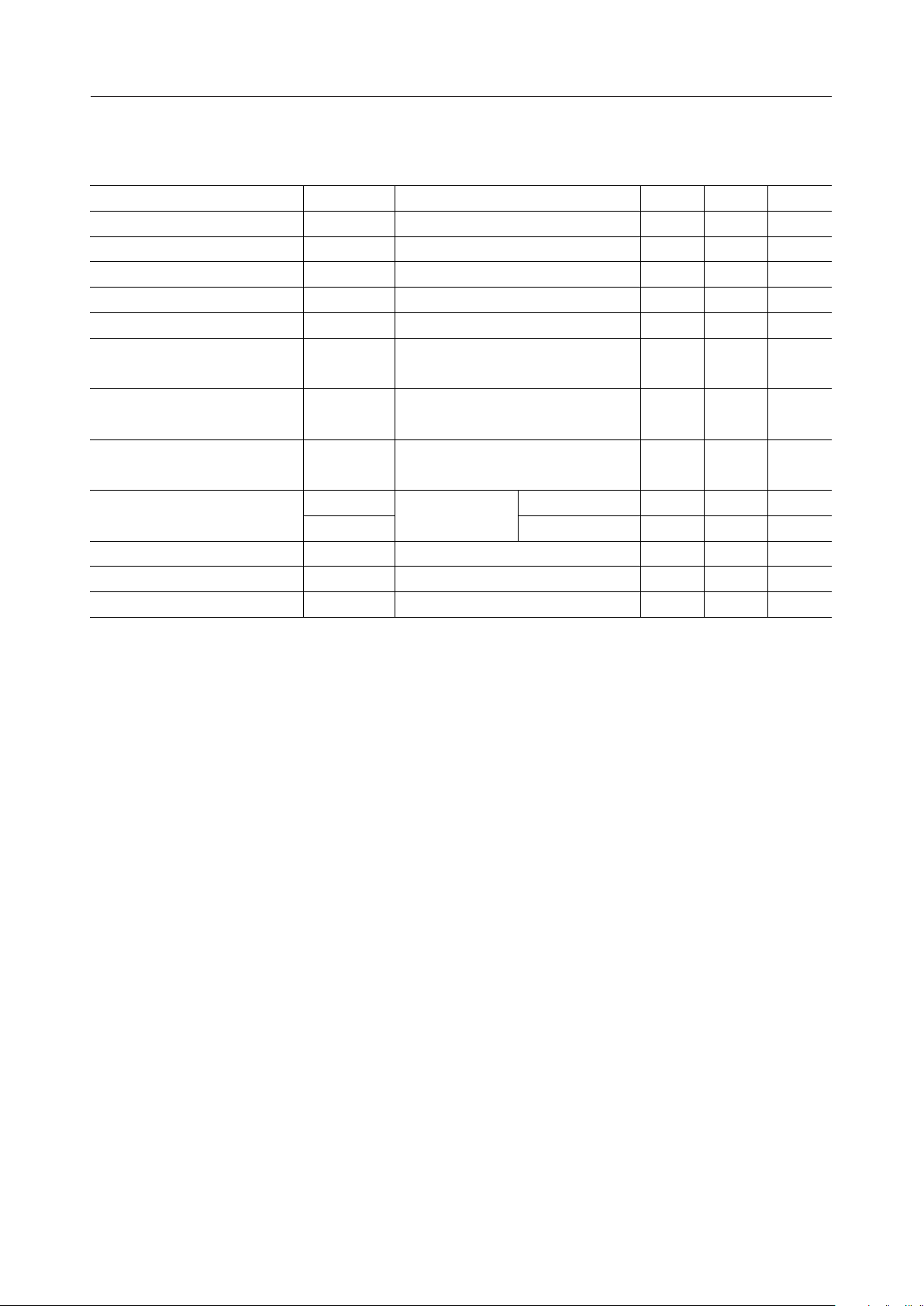
AC Characteristics
(Ta=–40 to +85°C, VDD=8.0 to 18.5V)
Parameter Symbol
Clock Frequency
Clock Pulse Width
Data Setup Time
Data Hold Time
CS Off Time
t
t
t
t
f
C
CW
DS
DH
CSL
R2=10kW±5%, C2=27pF±5% 20 — ms
CS Setup Time
t
(CS-Clock)
CSS
CS Hold Time
t
(Clock-CS)
CSH
DATA Output Delay Time
t
(Clock-DATA I/O)
Output Slew Rate Time
Rise Time
V
DD
V
Off Time Mounted in a unit, VDD=0.0V 5.0 — ms
DD
CS Wait Time — 400 — ms
PD
t
t
t
PRZ
t
POF
t
RSOFF
R
F
C
L
Condition Min. Max. Unit
— — 1.0 MHz
— 400 — ns
— 400 — ns
— 400 — ns
— 400 — ns
— 400 — ns
— — 1.0 ms
=20% to 80% — 4.0 ms
t
=100pF
R
=80% to 20% — 4.0 ms
t
F
Mounted in a unit — 100 ms
8/24
Page 9
¡ Semiconductor
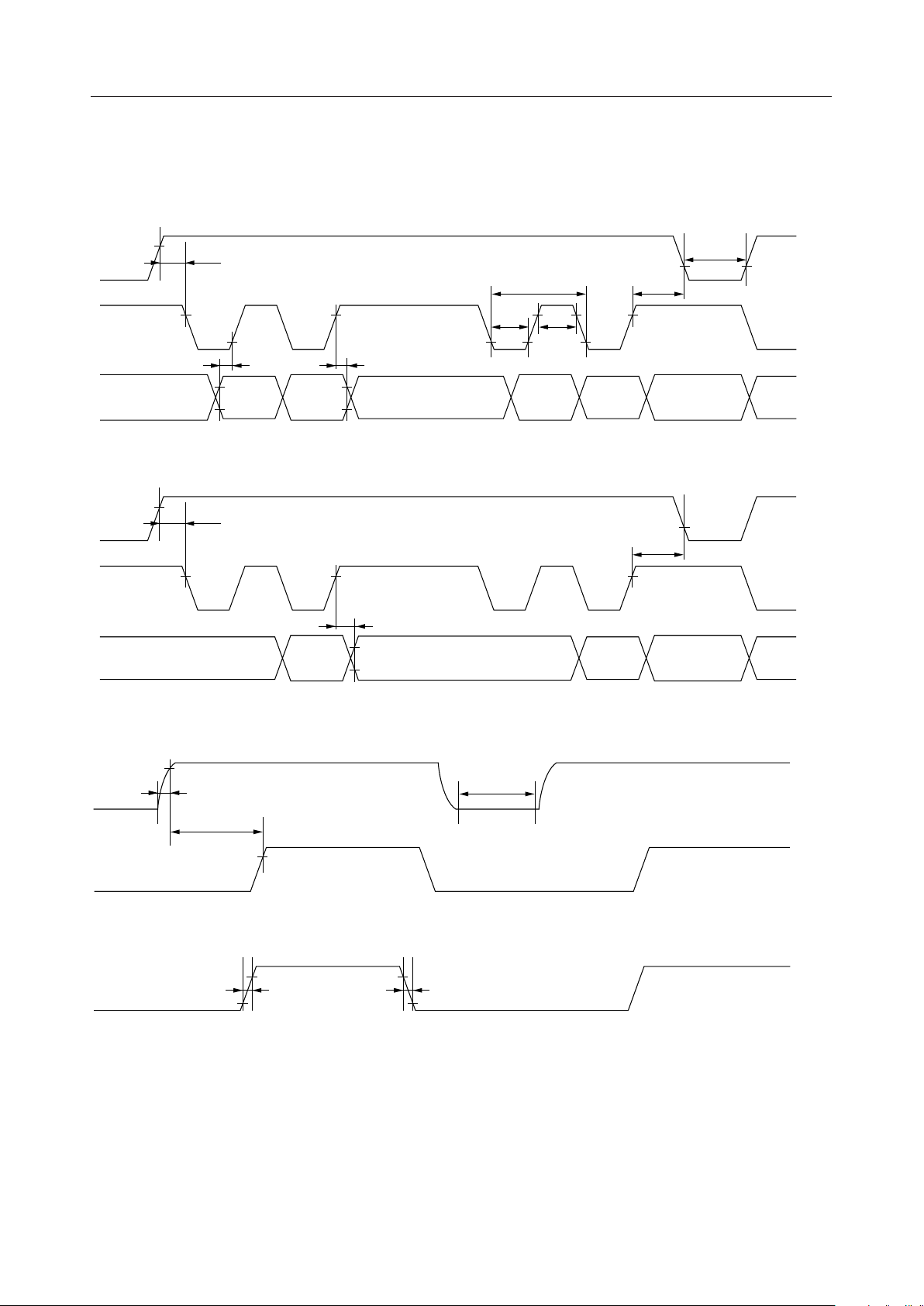
TIMING DIAGRAM
Data Input Timing
MSM9223
t
CS
CSS
CLOCK
t
DS
DATA I/O
(INPUT)
VALID VALID VALID VALID
Data Output Timing
t
CS
CLOCK
DATA I/O
(OUTPUT)
CSS
t
CSL
–3.8V
–0.8V
1/f
C
t
CW
t
CW
t
CSH
–3.8V
–0.8V
t
DH
–3.8V
–0.8V
–3.8V
–0.8V
t
CSH
–3.8V
–0.8V
t
PD
–3.8V
–0.8V
Reset Timing
t
V
DD
PRZ
t
RSOFF
CS
Driver Output Timing
SEG1-27, GRID1-3
–0.8V
t
POF
DD
–0.0V
–3.8V
–0.0V
–0.8V
–0.2V
DD
DD
t
R
t
F
9/24
Page 10
¡ Semiconductor
MSM9223
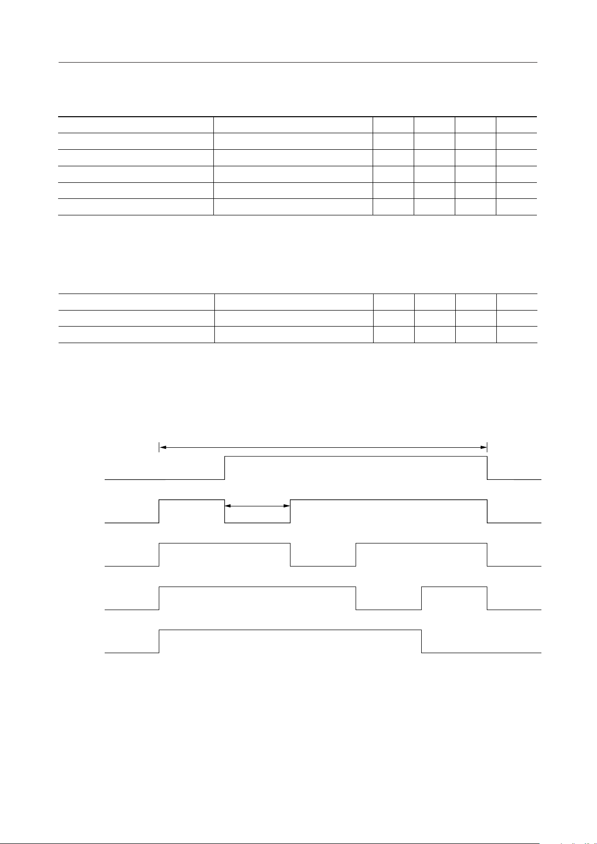
A/D Converter Characteristics
(Ta = –40 to +85°C, V
Parameter
A/D Conversion Accuracy
Reference Voltage (V
) — 5.0 5.5 V
REG
Output Current — — –10 mA
Input Voltage Range — — V
Conversion Time/Channel R2 = 10kW±5%, C2 = 27pF±5% 310
Condition Typ. Max. Unit
— — ±1 LSB
Min.
—
4.5
—
GND
256 394 ms
= 8.0 to 18.0 V)
DD
REG
Keyscan Characteristics
(Ta = –40 to +85°C, V
Parameter
Keyscan Cycle Time
R2 = 10kW±5%, C2 = 27pF±5% 194 246 ms
Keyscan Pulse Width R2 = 10kW±5%, C2 = 27pF±5% 39
Condition Typ. Max. Unit
Min.
160
32 49 ms
= 8.0 to 18.0 V)
DD
V
Keyscan Timing
ROW1
ROW2
ROW3
ROW4
ROW5
Keyscan Cycle Time
Keyscan Pulse
Width
10/24
Page 11
¡ Semiconductor
MSM9223
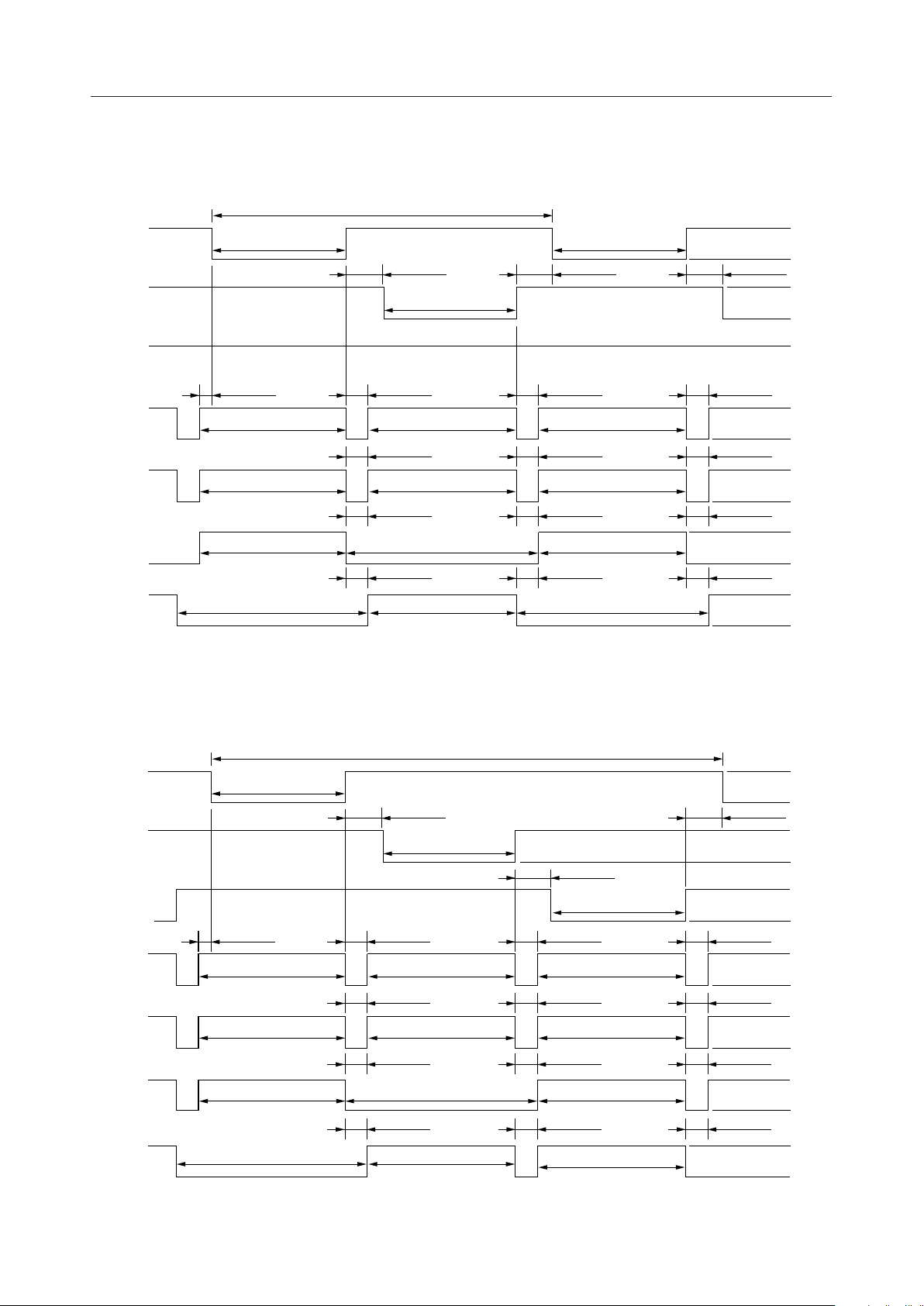
Output Timing (Duplex Operation) *1bit time=4/f
(The dimming data is 1016/1024)
2048bit times (1 display cycle)
GRID1
GRID2
GRID3
SEG1-27
DIM OUT
SYNC OUT1
SYNC OUT2
1016bit times 1016bit times
1016bit times
1019bit times1019bit times 1019bit times
1019bit times1019bit times 1019bit times
1029bit times1019bit times 1019bit times
1019bit times1029bit times 1029bit times
OSC
V
DD
8bit times8bit times8bit times
5bit times5bit times5bit times3bit times
5bit times5bit times5bit times
5bit times5bit times5bit times
5bit times5bit times5bit times
D-GND
V
DD
D-GND
V
DD
D-GND
V
DD
D-GND
5 V
L-GND
5 V
L-GND
5 V
L-GND
Output Timing (Triplex Operation) *1bit time=4/f
(The dimming data is 1016/1024)
3072bit times (1 display cycle)
GRID1
GRID2
GRID3
SEG1-27
DIM OUT
SYNC OUT1
SYNC OUT2
1016bit times
1016bit times
1019bit times1019bit times 1019bit times
1019bit times1019bit times 1019bit times
1029bit times1019bit times 1019bit times
1019bit times1029bit times
OSC
8bit times
1016bit times
1019bit times
V
DD
8bit times8bit times
5bit times5bit times5bit times3bit times
5bit times5bit times5bit times
5bit times5bit times5bit times
5bit times5bit times5bit times
D-GND
V
DD
D-GND
V
DD
D-GND
V
DD
D-GND
5 V
L-GND
5 V
L-GND
5 V
L-GND
11/24
Page 12
¡ Semiconductor
MSM9223
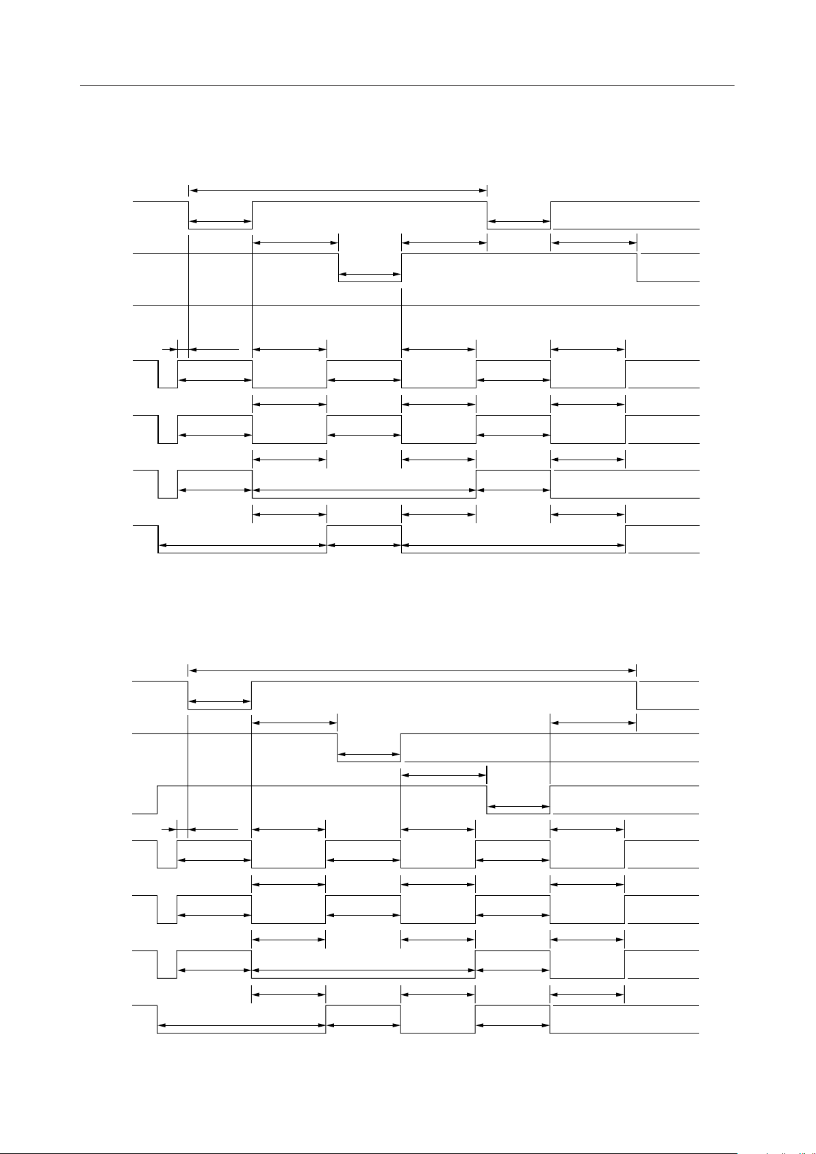
Output Timing (Duplex Operation) *1bit time=4/f
(The dimming data is 64/1024)
2048bit times (1 display cycle)
GRID1
GRID2
GRID3
SEG1-27
DIM OUT
SYNC OUT1
SYNC OUT2
64bit times
960bit times 960bit times 960bit times
64bit times
3bit times
67bit times
67bit times
67bit times
1981bit times 1981bit times
957bit times
67bit times
957bit times
67bit times
957bit times
1981bit times
957bit times
67bit times
957bit times
957bit times
957bit times
957bit times
OSC
64bit times
67bit times
67bit times
67bit times
957bit times
957bit times
957bit times
957bit times
V
DD
D-GND
V
DD
D-GND
V
DD
D-GND
V
DD
D-GND
5 V
L-GND
5 V
L-GND
5 V
L-GND
Output Timing (Triplex Operation) *1bit time=4/f
(The dimming data is 64/1024)
3072bit times (1 display cycle)
GRID1
GRID2
GRID3
SEG1-27
DIM OUT
SYNC OUT1
SYNC OUT2
64bit times
3bit times
67bit times
67bit times
67bit times
1981bit times
960bit times 960bit times
64bit times
960bit times
957bit times
67bit times
957bit times
67bit times
957bit times
1981bit times
957bit times
67bit times 67bit times
957bit times
957bit times
957bit times
957bit times
OSC
64bit times
67bit times
67bit times
67bit times
957bit times
957bit times
957bit times
957bit times
V
DD
D-GND
V
DD
D-GND
V
DD
D-GND
V
DD
D-GND
5 V
L-GND
5 V
L-GND
5 V
L-GND
12/24
Page 13
¡ Semiconductor
MSM9223
FUNCTIONAL DESCRIPTION
Power-on Reset
When power is turned on, MSM9223 is initialized by the internal power-on reset circuit.
The status of the internal circuit after initialization is as follows:
• The contents of the shift registers and latches are set to "0".
• The digital dimming duty cycle is set to "0".
• All segment outputs are set to Low level.
• All grid outputs are set to High level.
• All the ROW outputs are set to Low level.
• INT output is set to Low level.
Data Input and Output
Data input and output through the DATA-I/O pin is valid only when the CS pin is set at a High
level.
The input data to DATA I/O pin is shifted into the shift register at the rising edge of the serial
clock. The data is automatically loaded to the latches when the CS pin is set at a Low level.
10-bit dimming data (D1 to D10) and 27-bit segment data (S1 to S27) are used for inputting of
dimming data and display data. To transfer these two data, the mode data (M0 to M2) must be
sent after each of these data succeddingly.
The output data from the DATA I/O pin is output from the shift register at the rising edge of the
serial clock.
MSM9223 outputs 48-bit (6ch ¥ 8bits) A/D data (A11 to A68) and 29-bit key data (S11 to S55, R1
and Q1 to Q3). To receive these data, the mode data (M0 to M2) mast be sent first and then CS
must be set once to Low level and set again to High level.
Then inputting serial clocks, these data are output from the DATA I/O pin.
When the CS pin is set at a Low level, the DATA I/O pin returns to an input pin.
To stop the keyscan, the only mode data (M0 to M2) must be sent. After the mode data transfer,
the key scanning is stopped immediately.
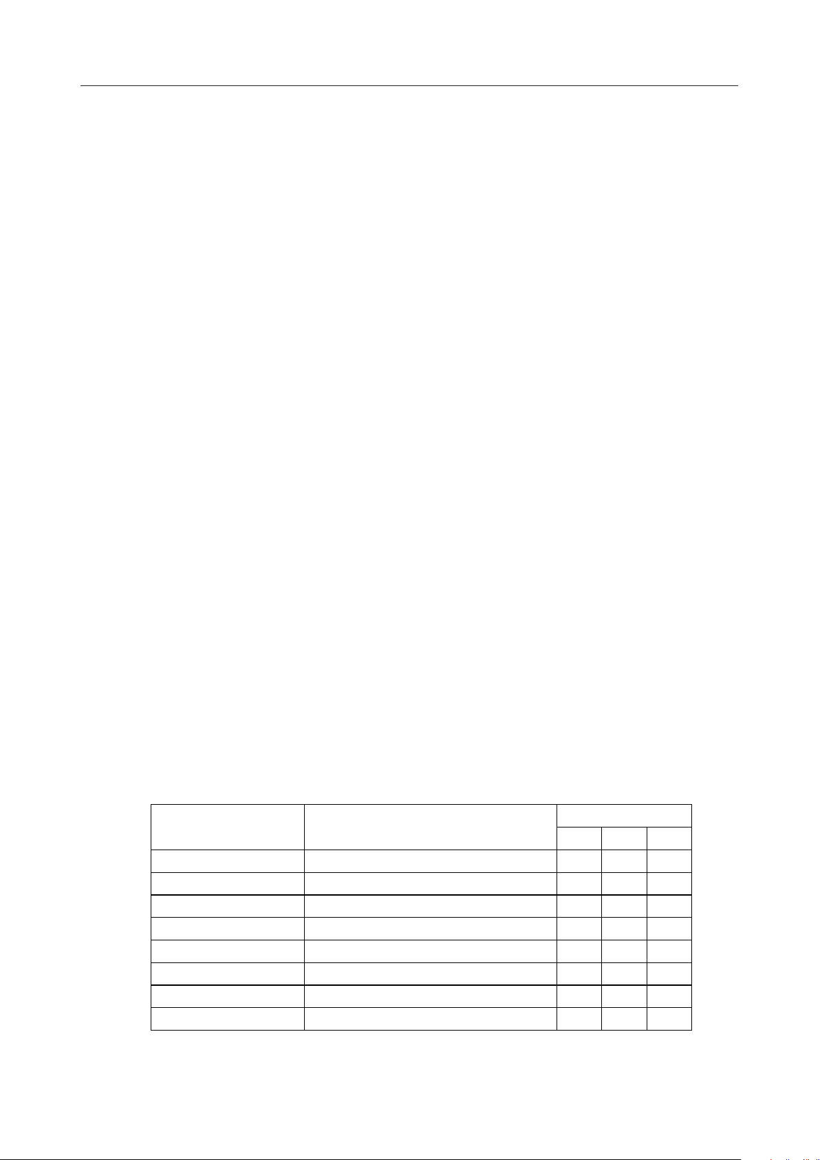
Mode Data
MSM9223 has the seven function modes. The function mode is selected by the mode data (M0 to
M2). The relation between function mode and mode data (M0 to M2) is as follows:
FUNCTION MODE OPERATING MODE
FUNCTION DATA
M0 M1 M2
0000 Segment Data for GRID1-3 Input
1001 Segment Data for GRID1 Input
0102 Segment Data for GRID2 Input
1103 Segment Data for GRID3 Input
0014 Digital Dimming Data Input
1015 Keyscan Stop
0116 Switch Data Output
1117 A/D Data Output
13/24
Page 14
¡ Semiconductor
MSM9223
Segment Data Input [Function Mode: 0 to 3]
• MSM9223 receives the segment data when function mode 0 to 3 are selected.
• The same segment data is transferred to the 3 segment data latch correspond to GRID 1 to 3 at
the same time when the function mode 0 is selected.
• The segment data is transferred to only one segment data latch that is selected by mode data,
when the function mode is 1, 2 or 3 is selected.
• Segment output (SEG1 to 27) becomes High level when the segment data (S1 to 27) is High level.
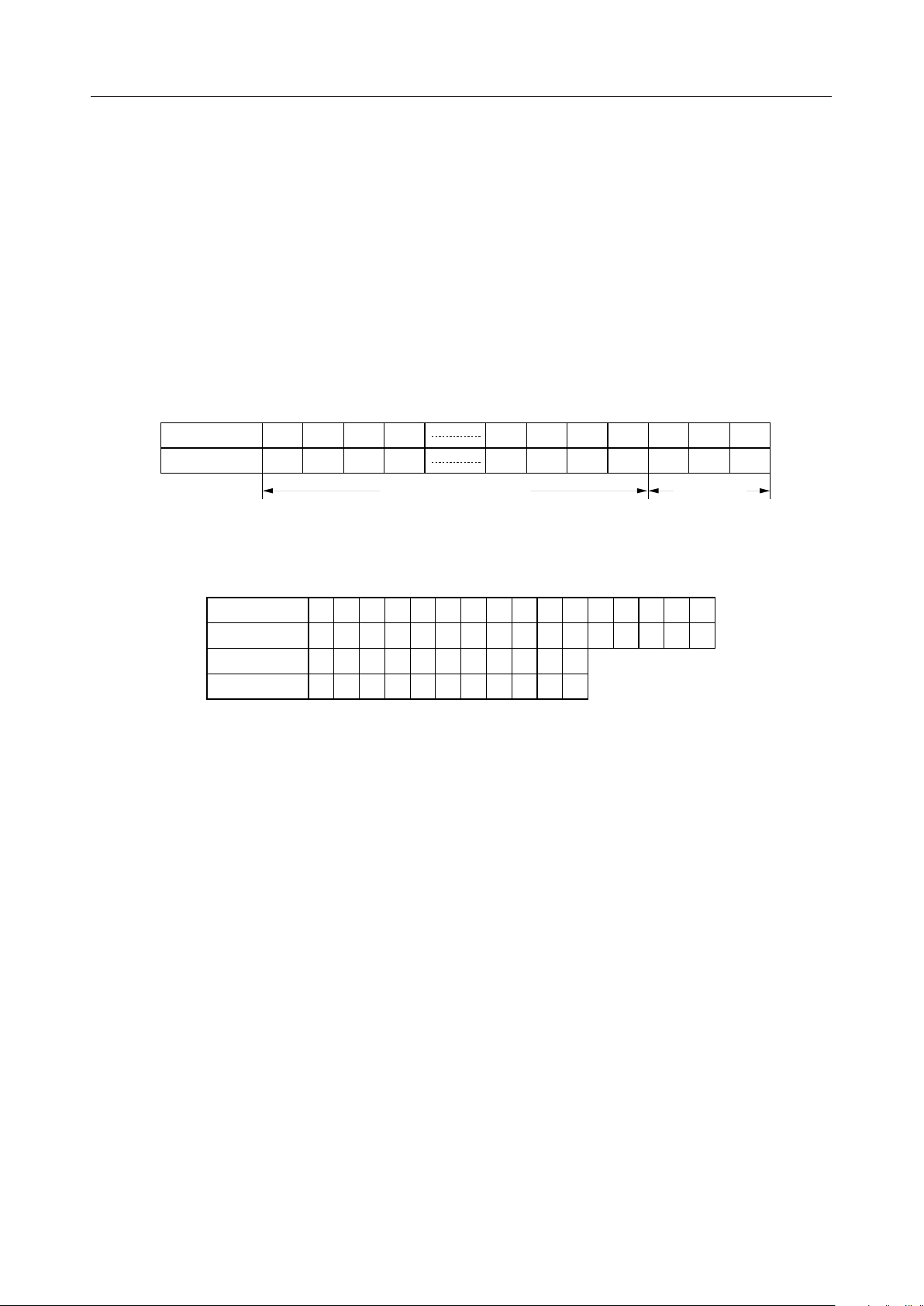
[Data Format]
Input Data : 30 bits
Segment Data : 27 bits
Mode Data : 3 bits
Bit
Input Data
1
S12S23S34S4
24
S2425S2526S2627S2728M029M130M2
Segment Data (27bits) Mode Data
[Bit correspondence between segment output and segment data]
1
2
3
4
5
6
7
8
9
10
S10
26
S26
11
S11
27
S27
SEG n
Segment data
SEG n
Segment data
S1
17
S17
S2
18
S18
S3
19
S19
S4
20
S20
S5
21
S21
S6
22
S22
S7
23
S23
S8
24
S24
S9
25
S25
(3bits)
12
S1213S1314S1415S1516S16
14/24
Page 15
¡ Semiconductor
MSM9223
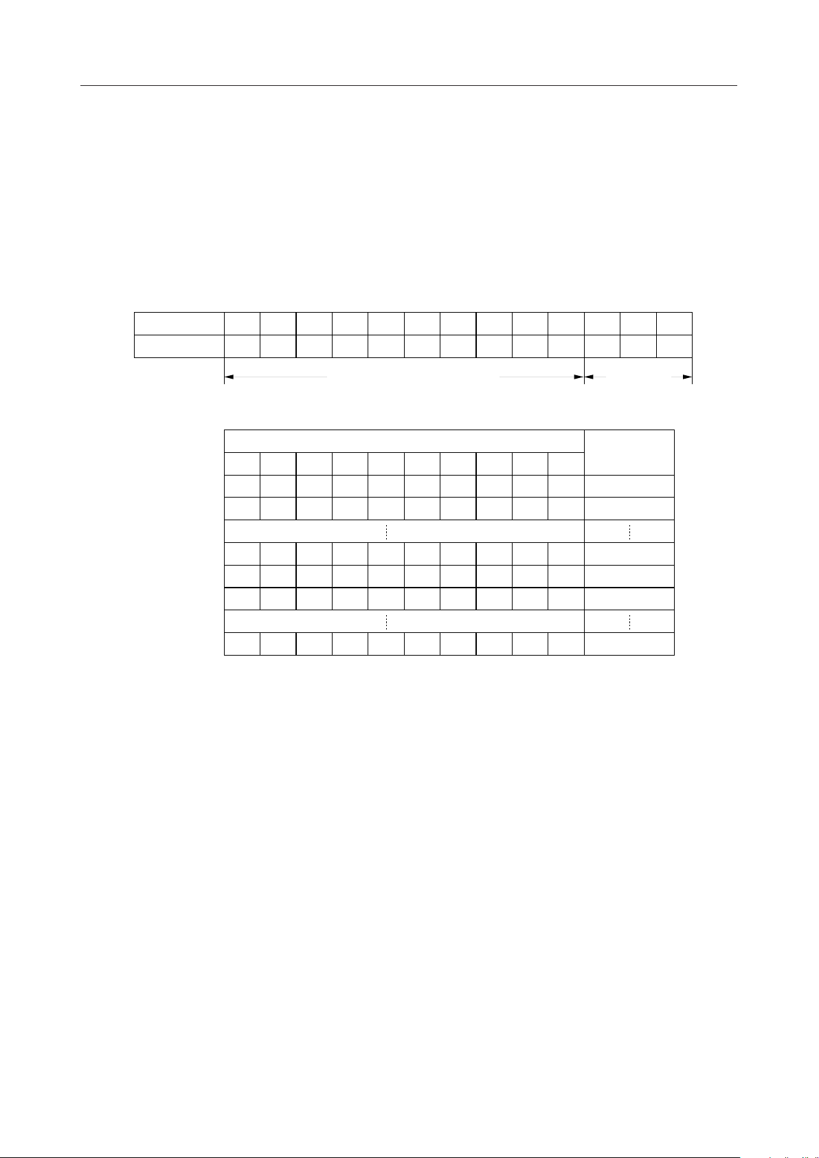
Digital Dimming Data Input [Function Mode: 4]
• MSM9223 receives the digital dimming data when function mode 4 is selected.
• The output duty changes in the range of 0/1024 (0%) to 1016/1024 (99.2%) for each grid.
• The 10-bit digital dimming data is input from LSB.
[Data Format]
Input Data : 13 bits
Digital Dimming Data: 10 bits
Mode Data : 3 bits
Bit
Input Data
1
D12D23D34D4
LSB MSB
D2
D1
0
0
0
1
1
1
0
0
0
1
1
1
Digital Dimming Data (10bits) Mode Data
D3
0
0
1
0
0
1
D4
0
0
0
1
1
1
5
D56D6
Dimming Data (MSB)(LSB)
D5
0
0
1
1
1
1
7
D78D89D910D1011M012M113M2
D10
D9
D8
D7
D6
0
0
0
0
0
0
0
0
0
0
1
1
1
1
1
1
1
1
1
1
1
1
1
1
1
1
1
1
1
1
(3bits)
Duty Cycle
0/1024
1/1024
1015/1024
1016/1024
1016/1024
1016/1024
15/24
Page 16
¡ Semiconductor
MSM9223
Keyscan Stop [Function Mode: 5]
• MSM9223 stops a key scanning when function mode 5 are selected.
• To select this mode, the only mode data (M0 to M2) is needed.
• The actual time lag range between receipt of the keyscan stop command and the ceasing of
scanning is 2.4ms to 3.6ms
[Input Data Format]
Input Data : 3 bits
Mode Data : 3 bits
Bit
Input Data
28M029M130
M2
Mode Data
(3bits)
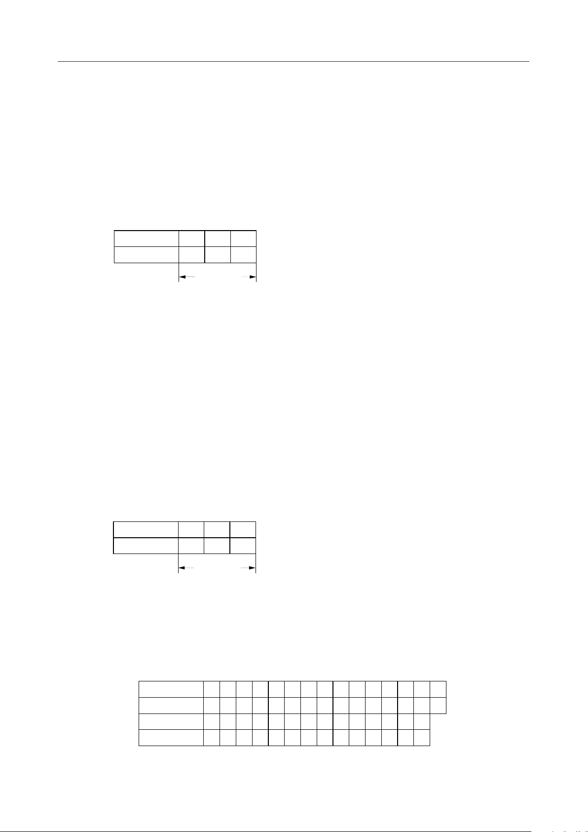
Switch Data Output [Function Mode: 6]
• MSM9223 output the switch data when function mode 6 is selected.
• To select this mode, the only mode data (M0 to M2) is needed.
• When MSM9223 recieves this mode, the DATA I/O pin is changed to an output pin.
• 29-bit switch data come out from the DATA I/O pin synchronizing with the rise edge of the
clock.
• When the CS pin is set at the low level, the DATA I/O pin returns to an input pin.
• R1=0, implies Right rotation of the knob (Clockwise)
• R1=1, implies Left rotation of the knob (Counter Clockwise)
• Contact Count bits are Q1 (LSB) to Q3 (MSB)
[Input Data Format]
Input Data : 3 bits
Mode Data : 3 bits
Bit
28M029M130
Input Data
[Output Data Format]
Output Data : 29 bits
5¥5 push swithc Data : 25 bits
Encoder switch Data : 4 bits
Bit
Output Data
Bit
Output Data
M2
Mode Data
(3bits)
1
2
3
4
5
6
S11
S12
S13
S14
S15
S21
S22
16
17
18
19
20
21
22
S41
S42
S43
S44
S45
S51
S52
Sij : i=ROW1 to 5, j=COL1 to 5
Sij=1 : Switch ON
Sij=0 : Switch OFF
7
8
9
10
11
12
13
14
15
S23
S24
S25
S31
S32
S33
S34
S35
23
24
25
26
27
28
29
S53
S54
S55
R1
Q1
Q2
Q3
16/24
Page 17
¡ Semiconductor
MSM9223
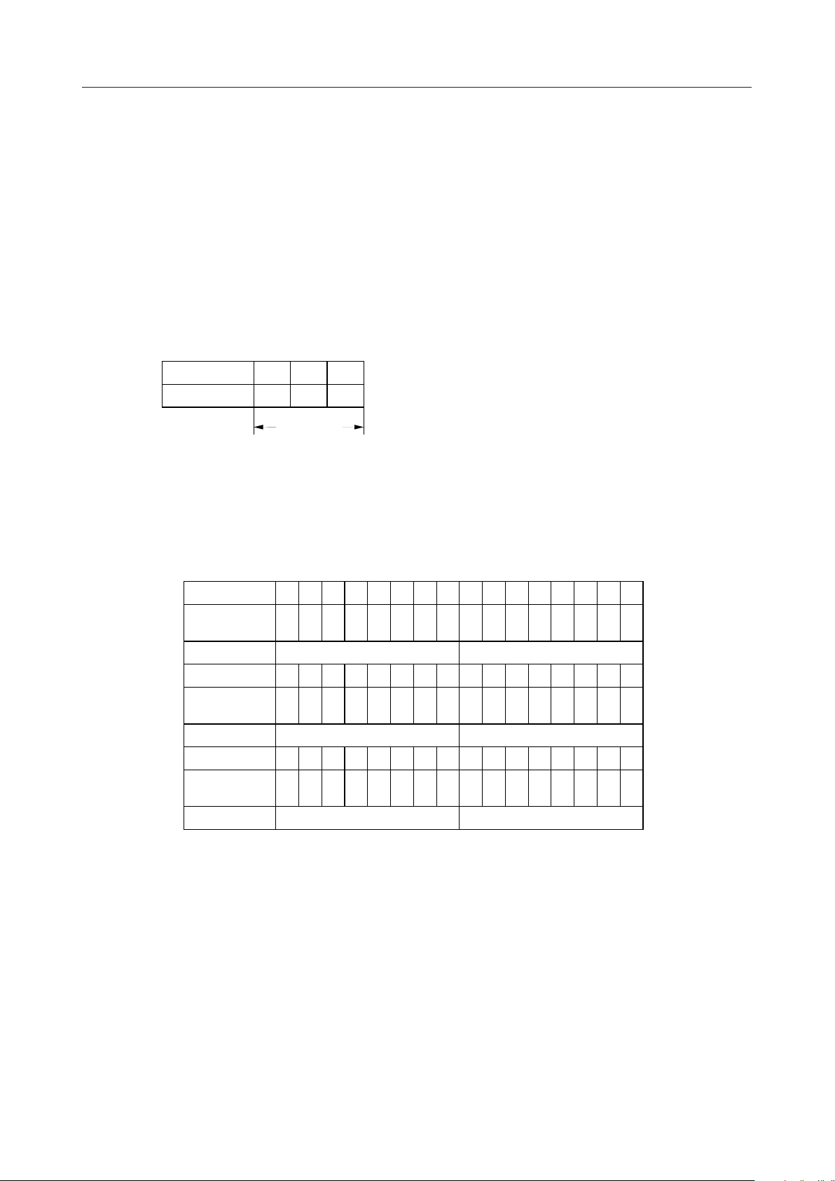
A/D Data Output [Function Mode: 7]
• MSM9223 output the A/D data when function mode 7 is selected.
• To select this mode, the only mode data (M0 to M2) is needed.
• When MSM9223 recieves this mode, the DATA I/O pin is changed to an output pin.
• 48-bit A/D data come out from the DATA I/O pin synchronizeing with the rise edge of the
clock.
• When the CS pin is set at the low level, the DATA I/O pin returns to an input pin.
[Input Data Format]
Input Data : 3 bits
Mode Data : 3 bits
Bit
28M029M130
Input Data
[Output Data Format]
Output Data : 48 bits
A/D Data : 48 bits
Bit
Output Data
A/D
Output Data
A/D
Output Data
A/D
Mode Data
(3bits)
1
2
A11
A123A134A14
(LSB)
17 18
A31
A3219A3320A34
(LSB)
33 34
A51
A5235A5336A54
(LSB)
M2
5
A156A167A178A18
CH1
21
A3522A3623A37
CH3
37
A5538A5639A57
CH5
9
A21
(MSB)
(LSB)
24 25 26
A38
A41
(MSB)
(LSB)
40 41 42
A58
A61
(MSB)
(LSB)
10
A2211A2312A24
A4227A4328A44
A6243A6344A64
13
A2514A2615A2716A28
CH2
29
A4530A4631A47
CH4
45
A6546A6647A67
CH6
(MSB)
32Bit
A48
(MSB)
48Bit
A68
(MSB)
17/24
Page 18
¡ Semiconductor
MSM9223
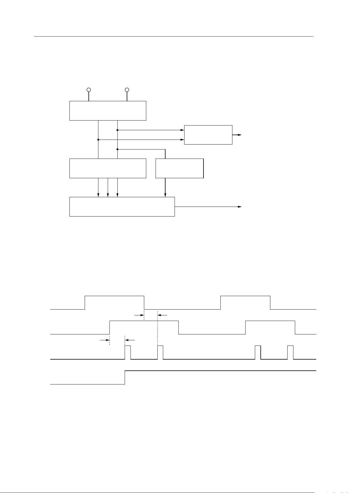
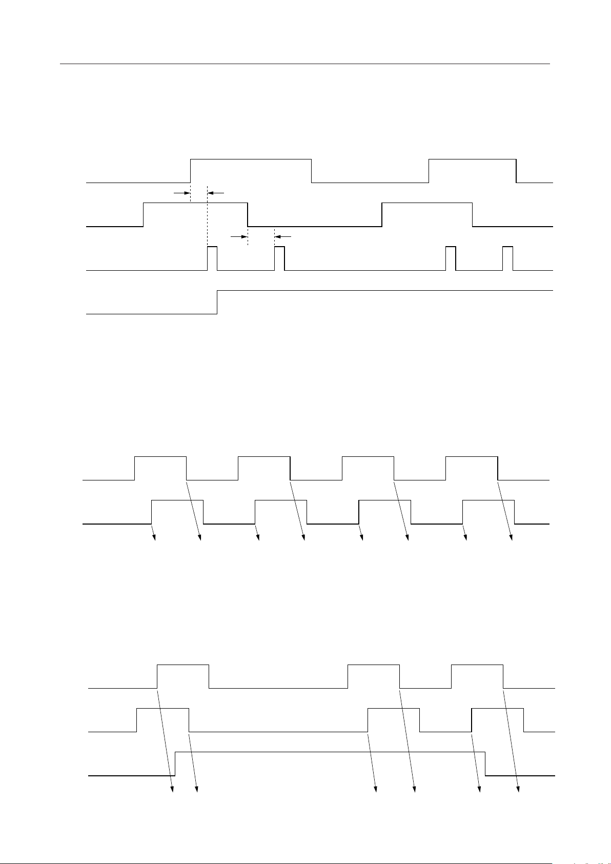
The rotary encoder switch function.
As figure 1 shows, the rotary encoder switch circuit is consisted of Phase detection, Interrupt
generation, Up/down counter, Direction latch and Parallel-in serial-out shift register.
A
Phase Detection
UP DOWN
UP/DOWN Counter
Q3 Q2 Q1
P-in/S-out Shift Registor
B
Interrupt
Generation
Direction Latch
R1
for INT
Output data
Fig.1 The Rotary Encoder Switch Circuit
1) Phase detection
1-1) Clockwise
The input A and B have a chattering absorption circuit of 620ns (typ.). When signal A and B input
as fig. 2, the phase detection circuit outputs UP signal after the chattering absorption period. At
this time, the output INT also goes to high level, so this signal can be used as an interrupt. The
INT stays High level until the switch data-output mode is selected.
A
B
UP (internal)
INT
chattering absorption time
Fig.2 The Input and Output Timing in Case of Clockwise.
18/24
Page 19
¡ Semiconductor
MSM9223
1-2) counter clockwise
When signal A and B input as fig. 3, the phase detection circuit outputs Down signal after the
chattering absorption period. At this time, the output INT also goes to High level. The INT stays
High level until the switch data-output mode is selected.
A
chattering absorption time
B
DOWN (internal)
INT
Fig.3 The Input and Output Timing in Case of Counter Clockwise.
2) UP/DOWN COUNTER
When the UP/DOWN COUNTER is input UP, it counts up and when it is input DOWN, it counts
down.
But if overcounte of "111" occurs the UP/DOWN COUNTER stays "111".
A
B
Q3, Q2, Q1
001 010 011 100 101 110 111 111
Fig.4
3) Direction latch
When the Direction latch is input DOWN the output R goes "1". But if the UP pulse is input and
the counts value change to plus value, the output R goes to "0".
A
B
R1
Q1, Q2, Q3
010 100 100100 000 010
Fig.5
19/24
Page 20
¡ Semiconductor
MSM9223
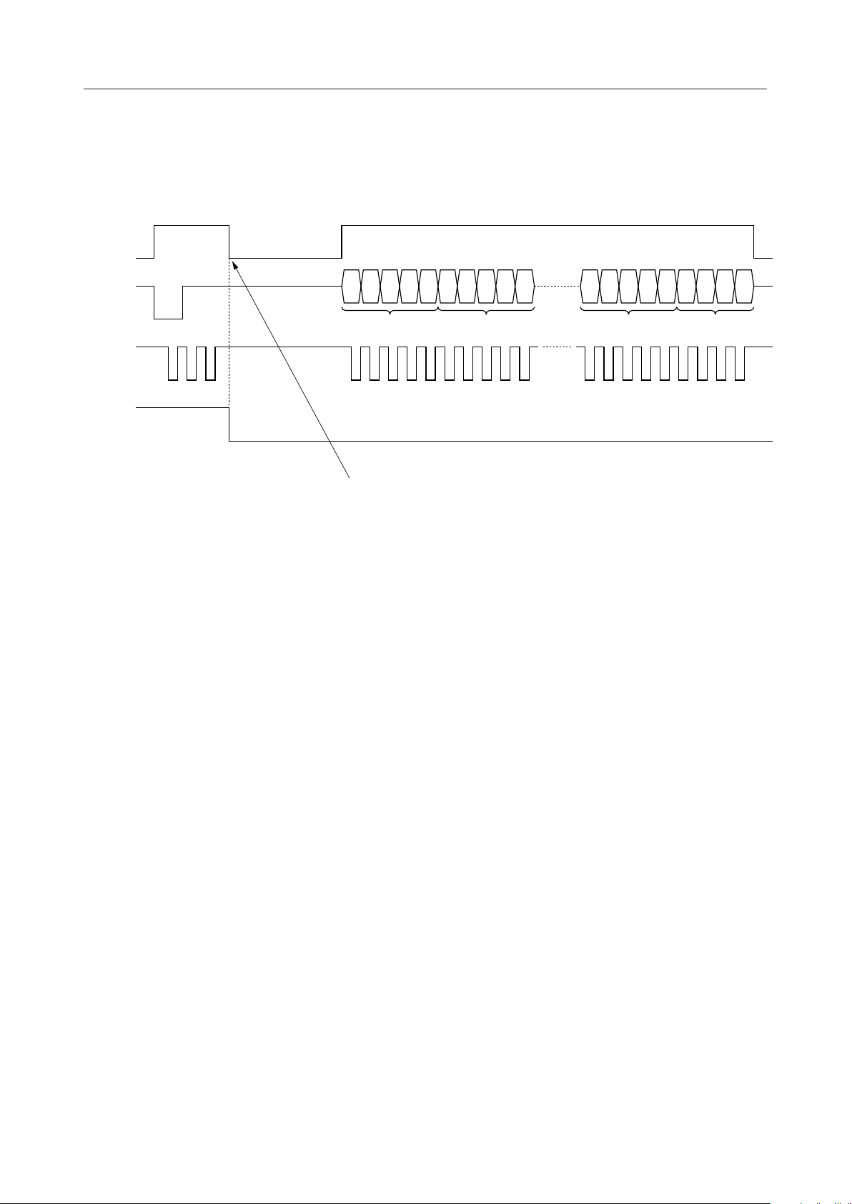
4) P-in/S-out shift resistor
When the switch data output mode is selected and SC goes L, all the key data send to the shift
resistor, and the up/down counter is reset and the INT signal goes "L".
CS
Data I/O
CLOCK
INT
C2C1 C4 C5C3
ROW1
When CS goes L, the up/down counter is reset and the INT goes "L".
C2C1 C4 C5C3
ROW2
Fig.6
C2C1 C4 C5C3
ROW5
Q1R1 Q3Q2
Rotary
20/24
Page 21
¡ Semiconductor
MSM9223
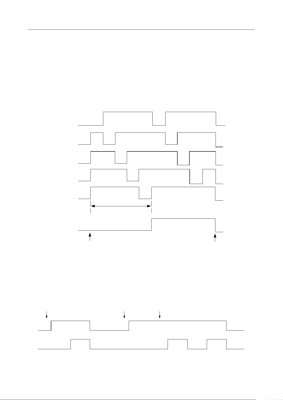
Keyscan
Keyscanning is started only when depression or release of any key is detected in order to
minimize noise caused by scanning signal. Then, keyscanning is continued until the keyscan
stop mode is sent from a microcomputer. The INT pin goes to the high level at the completion
of 1-cycle scanning after the keyscan start, so the (high level) signal sent from the INT pin can be
used as an interrupt signal.
[Keyscan Timing]
ROW 0
ROW 1
ROW 2
ROW 3
ROW 4
1 Cycle
INT
Depress/Release
Keyscan stop mode
is selected.
Note: Keyscanning cannot be stopped by selecting the keyscan stop mode only once if:
- keyscanning is started after depression or release of any key is detected, and then
- a key is depressed or released again before the keyscan stop mode is selected.
To stop keyscanning, it is required to select the keyscan stop mode once again.
Depress Depress Release
INT
CS
Keyscan Keyscan
MODE5
MODE5 : Keyscan stop
MODE5MODE5
21/24
Page 22
¡ Semiconductor
MSM9223
22/24
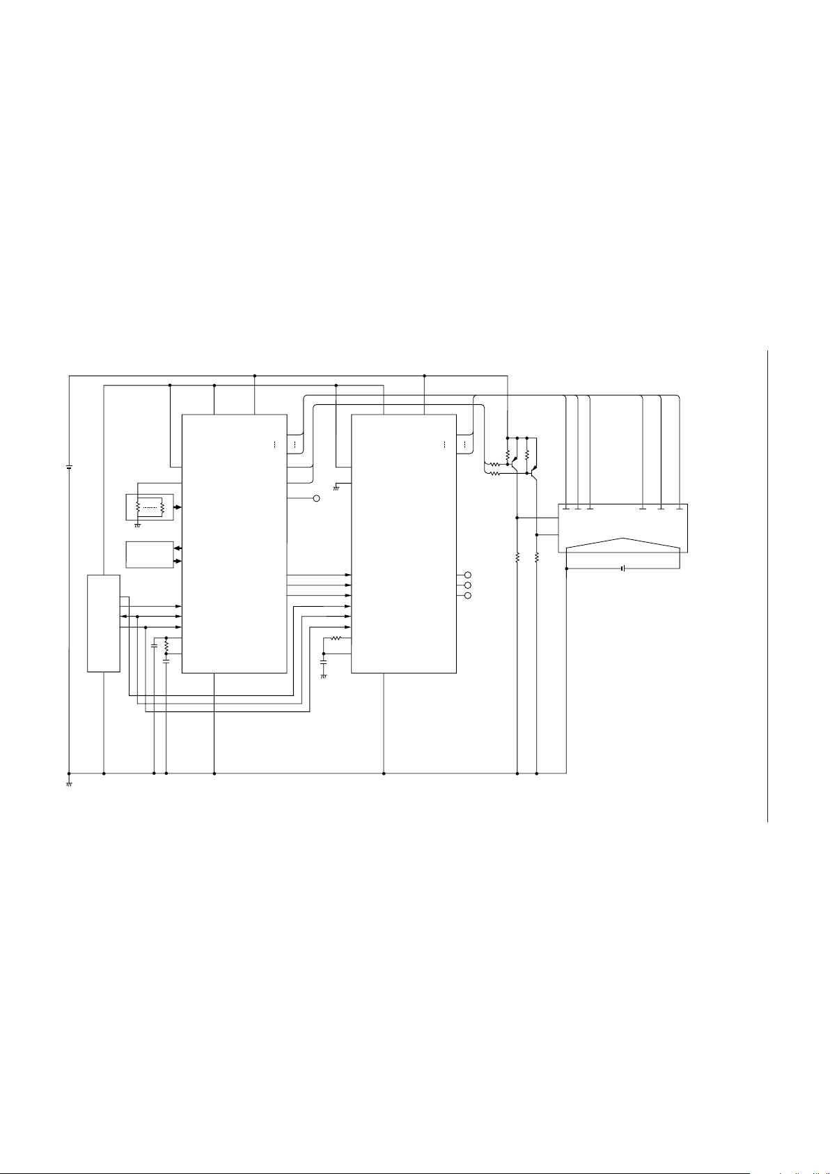
APPLICATION CIRCUITS
1. Circuit for the duplex VFD tube with 118 segments (2 Grid ¥ 59 Anode)
MSM9223
V
DD
V
CC
L-GND
OSC0
V
CC
CLOCK
DATA I/O
CS
VREG
DUP/TRI
DIM OUT
SYNC OUT 1
SYNC OUT 2
GRID2
GRID1
GRID3
SEG1
SEG27
MSM9210
(SLAVE)
V
DISP
V
DD
L-GND
OSC 0
OSC 1
CLOCK
DATA IN
CS
DIM IN
SYNC IN 1
SYNC IN 2
DIM OUT
SYNC OUT 1
SYNC OUT 2
GRID2
GRID1
GRID3
SEG1
SEG32
Duplex VFD Tube
S57 S58 S59
S1 S2 S3
G1
G2
Microcontroller
V
DISP
M/S
GND
DUP/TRI
Ef
GND
GND
GND
GND
CH1 to 6
ROW1 to 5
COL1 to 5
5 ¥ 5
Key matrix
Page 23
¡ Semiconductor
MSM9223
23/24
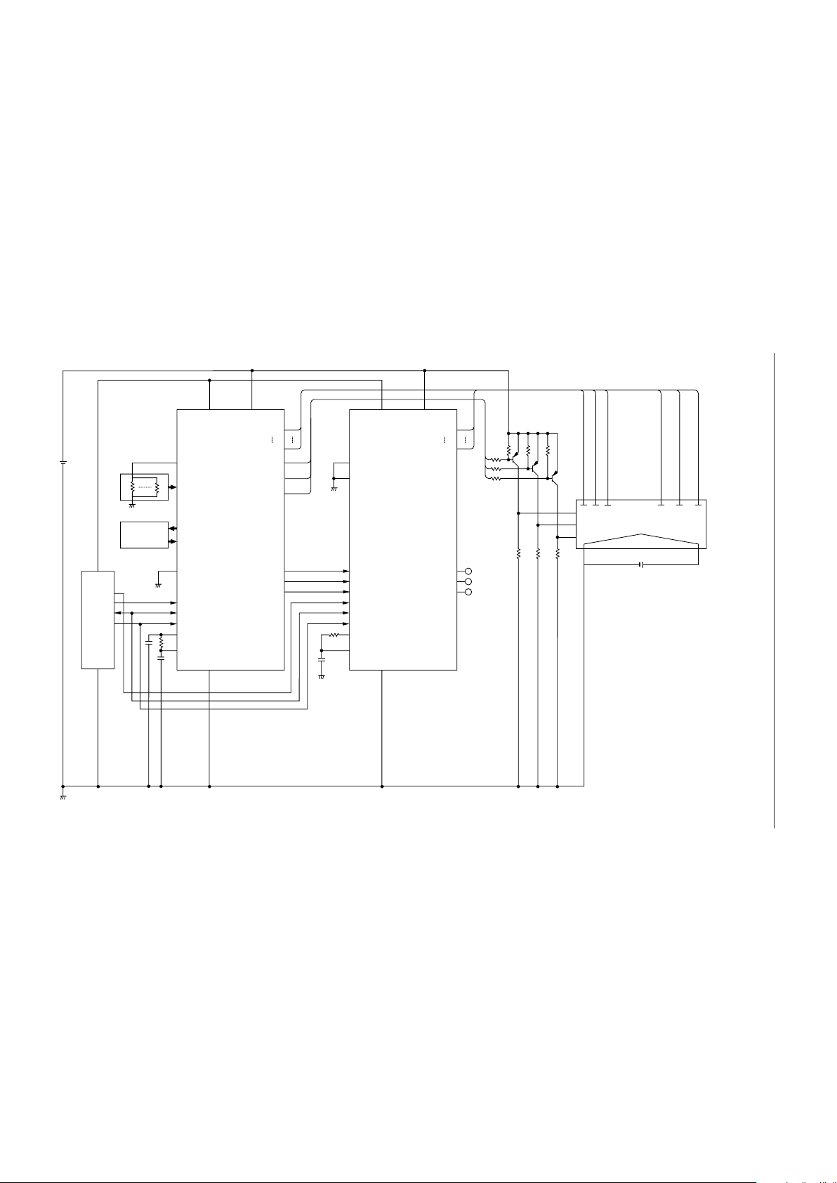
2. Circuit for the triplex VFD tube with 177 segments (3 Grid ¥ 59 Anode)
MSM9223
V
DD
V
CC
L-GND
CLOCK
DATA I/O
CS
DIM OUT
SYNC OUT 1
SYNC OUT 2
GRID2
GRID1
GRID3
SEG1
SEG27
MSM9210
(SLAVE)
V
DISP
V
DD
L-GND
OSC 0
OSC 1
CLOCK
DATA IN
CS
DIM IN
SYNC IN 1
SYNC IN 2
M/S
DUP/TRI
DIM OUT
SYNC OUT 1
SYNC OUT 2
GRID2
GRID1
GRID3
SEG1
SEG32
Triplex VFD Tube
S57 S58 S59
S1 S2 S3
G1
G2
Microcontroller
V
DISP
GND
Ef
GND
GND
GND
OSC0
V
CC
GND
CH1 to 6
ROW1 to 5
COL1 to 5
5 ¥ 5
Key matrix
VREG
G3
DUP/TRI
Page 24
¡ Semiconductor
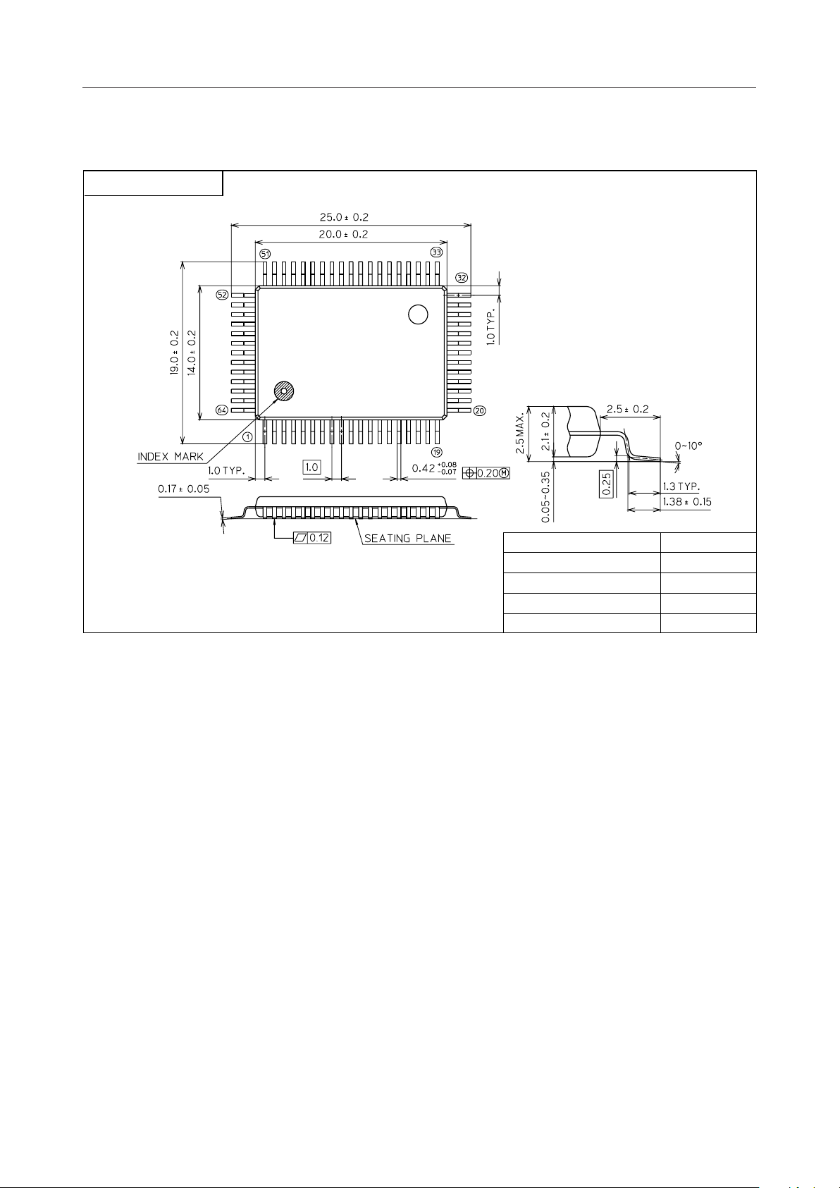
PACKAGE DIMENSIONS
QFP64-P-1420-1.00-BK
Mirror finish
MSM9223
(Unit : mm)
Package material
Lead frame material
Pin treatment
Solder plate thickness
Package weight (g)
Epoxy resin
42 alloy
Solder plating
5 mm or more
1.25 TYP.
Notes for Mounting the Surface Mount Type Package
The SOP, QFP, TSOP, SOJ, QFJ (PLCC), SHP and BGA are surface mount type packages, which
are very susceptible to heat in reflow mounting and humidity absorbed in storage.
Therefore, before you perform reflow mounting, contact Oki’s responsible sales person for the
product name, package name, pin number, package code and desired mounting conditions
(reflow method, temperature and times).
24/24
Page 25

E2Y0002-29-62
NOTICE
1. The information contained herein can change without notice owing to product and/or
technical improvements. Before using the product, please make sure that the information
being referred to is up-to-date.
2. The outline of action and examples for application circuits described herein have been
chosen as an explanation for the standard action and performance of the product. When
planning to use the product, please ensure that the external conditions are reflected in the
actual circuit, assembly, and program designs.
3. When designing your product, please use our product below the specified maximum
ratings and within the specified operating ranges including, but not limited to, operating
voltage, power dissipation, and operating temperature.
4. Oki assumes no responsibility or liability whatsoever for any failure or unusual or
unexpected operation resulting from misuse, neglect, improper installation, repair, alteration
or accident, improper handling, or unusual physical or electrical stress including, but not
limited to, exposure to parameters beyond the specified maximum ratings or operation
outside the specified operating range.
5. Neither indemnity against nor license of a third party’s industrial and intellectual property
right, etc. is granted by us in connection with the use of the product and/or the information
and drawings contained herein. No responsibility is assumed by us for any infringement
of a third party’s right which may result from the use thereof.
6. The products listed in this document are intended for use in general electronics equipment
for commercial applications (e.g., office automation, communication equipment,
measurement equipment, consumer electronics, etc.). These products are not authorized
for use in any system or application that requires special or enhanced quality and reliability
characteristics nor in any system or application where the failure of such system or
application may result in the loss or damage of property, or death or injury to humans.
Such applications include, but are not limited to, traffic and automotive equipment, safety
devices, aerospace equipment, nuclear power control, medical equipment, and life-support
systems.
7. Certain products in this document may need government approval before they can be
exported to particular countries. The purchaser assumes the responsibility of determining
the legality of export of these products and will take appropriate and necessary steps at their
own expense for these.
8. No part of the contents contained herein may be reprinted or reproduced without our prior
permission.
9. MS-DOS is a registered trademark of Microsoft Corporation.
Copyright 1999 Oki Electric Industry Co., Ltd.
Printed in Japan
 Loading...