

Page 1

FEDL9841-04
FEDL9841-04
¡ Semiconductor
This version: Jul. 2000
Previous version: Jun. 1999
MSM9841¡ Semiconductor
MSM9841
Recording and Playback LSI with Built-in FIFO
This document contains minimum specifications. For full specifications, please contact your
nearest Oki office or representative.
GENERAL DESCRIPTION
The MSM9841 is a mono/stereo record and playback LSI with a built-in 1K bit FIFO for easy
interface with external systems or non-semiconductor memory. It utilizes multiple record and
playback modes, including the new ADPCM2 algorithm, which allows for even higher quality
sound reproduction. The record and playback functions of the MSM9841 is controlled by an
MCU via 8/16-bit bus interface.
FEATURES
• 16/8-bit bus interface support
• FIFO capacity: User-definable (256/512/1024 bits)
(buffering time of 32 ms when using 8 kHz sampling frequency, 4-bit ADPCM2/ADPCM, and
in monaural playback)
• Supports four compression algorithms for record and playback:
4, 5, 6, 7, 8-bit ADPCM2; 4-bit ADPCM; 8; 16-bit PCM; and 8-bit Nonlinear PCM
• Sampling frequency: 4.0 kHz, 6.4 kHz, 8.0 kHz, 12.8 kHz, 16.0 kHz, 32.0 kHz* (fosc=4.096 MHz)
• Sampling frequency: 22.05 kHz*, 44.1 kHz* (fosc=5.6448 MHz)
• For the built-in ADC, set the sampling frequency at 16 kHz or less.
• DMA interface support
• Volume control (8 steps: 0 dB to –21 dB)
• Built-in 14-bit A/D converter
• Built-in 14-bit D/A converter
• Built-in low pass filter (LPF) : (input side: analog LPF)
: (output side: digital LPF)
• Power supply voltage: 2.7 V to 5.5 V
• Package:
56-pin plastic QFP (QFP56-P-910-0.65-2K) (Product name: MSM9841GS-2K)
*note 32 kHz, 22.05 kHz and 44.1 kHz are available only for playback.
1/9
Page 2
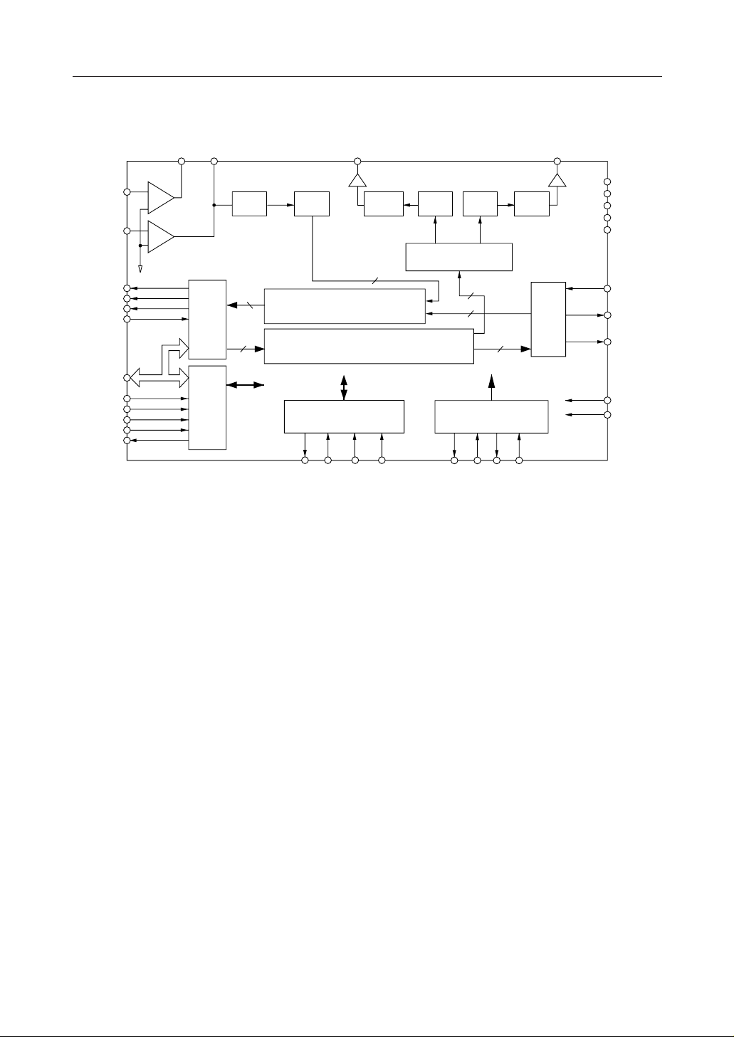
BLOCK DIAGRAM
MOUT LOUT AOUTL AOUTR
FEDL9841-04
MSM9841¡ Semiconductor
MIN
LIN
EMP
MID
FUL/DREQR
CH/DACKR
D15 to D0
WR
RD
CS
D/C
BUSY
FIFO
MCU
I/F
input side
LPF
Analyzer
Synthesizer
DMA I/F
output side
LPF
DAC DAC
Volume Controller
ADC
ADPCM2/ADPCM/PCM
ADPCM2/ADPCM/PCM/Non-linear PCM
DREQL DACKL IOW IOR
output side
LPF
Timing Controller
VCK XT XT RESET
External
DAC/ADC I/F
SG
AV
DD
AGND
DV
DD
DGND
ADSD
DASD
SIOCK
TEST0
TEST1
2/9
Page 3
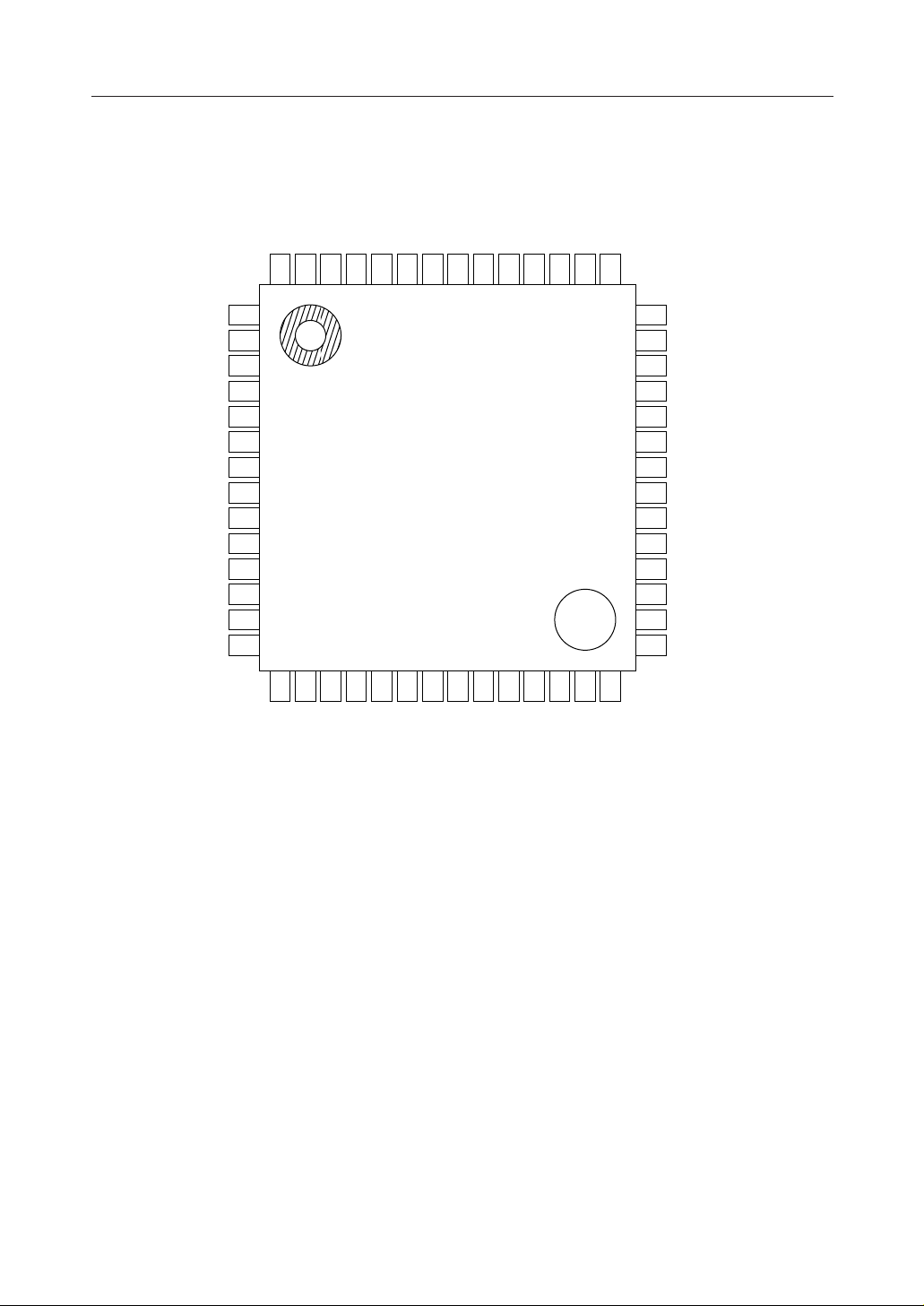
PIN CONFIGURATION (TOP VIEW)
FEDL9841-04
MSM9841¡ Semiconductor
D0
D1
D2
D3
NC
D4
D5
D6
D7
NC
D8
D9
D10
D11
XTXTIOR
56NC55545352515049484746454443
1
2
3
4
5
6
7
8
9
10
11
12
13
14
15NC16171819202122232425262728
D12
D13
D14
IOW
D15
DREQL
DACKL
NC
DGND
DGND
AGND
TEST1
TEST0
MIN
MOUT
VCK
LIN
ADSD
LOUT
DASD
SG
SIOCK
42
41
40
39
38
37
36
35
34
33
32
31
30
29
OUTL
BUSY
D/C
CS
RD
WR
FUL/DREQR
MID
EMP
CH/DACKR
RESET
NC
DV
DD
AV
DD
AOUTR
NC : No Connection
56-pin plastic QFP
3/9
Page 4

PIN DESCRIPTIONS
Symbol Type Description
For 8-bit bus interface, the command allows these pins to be configured to be inputs or outputs
to input or output data to and from an external memory. Otherwise, these pins are configured
D15-D8 I/O
D7-D0 I/O
WR I
RD I
CS I
D/C I
BUSY O
EMP O
MID O
FUL/DREQR O
CH/DACKR I
DREQL O
DACKL I
to be inputs only.
For 16-bit interface, these pins are a bidirectional data bus to input or output data to and from
an external microcontroller and memory.
Birirectional data bus to input or output data and output status to and from an external
microcontroller and memory.
Write pulse input pin. This pin pulses "L" when command or voice data is input to D15-D0 pins.
Read pulse input pin. This pin pulses "L" when status or voice data is output to D15-D0 pins.
Accepts write pulse and read pulse when this pin is "L". Does not accept write pulse and read
pulse when this pin is "H".
Voice data is input or output to and from D15-D0 pins when this pin is "H". Command is input
to and status is output from D7-D0 pins when this pin is "L".
This pin outputs a "L" level during RECORDING, PLAYBACK or PAUSE.
"H" level indicates that there is no data in FIFO memory. Active "H" can be changed to active "L"
by command input.
"H" level indicates that more than half of the FIFO memory space is filled with data.
During playback, voice synthesis starts when MID changes to "H" level. Active "H" can be
changed to active "L" by command input. This pin outputs a synchro signal for voice data input/
output when non-use of FIFO is selected.
"H" level indicates that FIFO memory is full of data. During playback, this pin is "H" and data
cannot be written in FIFO memory. Active "H" can be changed to active "L" by command input.
When DMA transfer and stereo playback are selected, "H" level DREQR outputs a signal to
request a DMA transfer. Active "H" can be changed to active "L" by command input.
When stereo playback is selected and CH is "H", the EMP, MID or FUL pin outputs the status of
right FIFO memory. When CH is "L", the EMP, MID or FUL pin outputs the status of left FIFO
memory. Set this pin to "L" during recording and monophonic playback. When DMA transfer
and stereo playback are selected, DACKR is selected. In this case, input a DMA transfer
acknowledge signal to DACKR. When DACKR is "L", the IOW signal is accepted. Active "L" can
be changed to active "H" by command input.
When DMA transfer is selected, "H" level DREQL outputs a signal to request a DMA transfer.
When stereo playback is selected, "H" level DREQL outputs a signal to request a DMA transfer.
Active "H" can be changed to active "L" by command input.
Input to DACKL a signal when DMA transfer is permitted by the DMA controller. When DACKL
is "L", IOR and IOW signals are accepted. When stereo playback is selected, input to DACKL a
DMA transfer acknowledge signal for left FIFO memory. Active "L" can be changed to active "H"
by command input. If DMA transfer is not used, set this pin to "H" level.
FEDL9841-04
MSM9841¡ Semiconductor
4/9
Page 5

PIN DESCRIPTIONS
Symbol Type Description
IOW I
IOR I
ADSD I
DASD O
SIOCK O
XT
XT
VCK O
RESET I
TEST0
TEST1
SG O
MIN
LIN
MOUT
LOUT
AOUTL O
AOUTR O
DV
DD
DGND —
AV
DD
AGND
Write pulse input pin to write external memory data to MSM9841 during DMA transfer.
If DMA transfer is not used, set this pin to "H" level.
Read pulse input pin to read data of MSM9841 during DMA transfer.
If DMA transfer is not used, set this pin to "H" level.
16-bit serial data input pin when external ADC is used. If external ADC is not used,
set this pin to "L" level.
16-bit serial data output pin when external DAC is used.
Synchronizing clock for 16-bit serial data input/output when external ADC or DAC is used.
I
Oscillator connection pins. When external clock is used, input clock into XT pin and leave XT
O
pin open.
Outputs sampling frequency selected at recording or playback.
VCK pin is used as a synchronizing signal when external ADC or DAC is used.
When this pin is "L" level input, the LSI is initialized.
Pins for testing. Set the pins to "L".
I
Analog circuit signal ground output pin.
Inverting input pin for built-in OP amplifier. Noninverting input pin is connected to SG (Signal
I
Ground) internally.
MOUT is the output of internal OP amplifier to MIN, and LOUT is to LIN.
O
Left analog output pin from built-in LPF. This is the output pin of playback wavefroms, and is
connected to the amplifier for driving speakers.
Right analog output pin from built-in LPF. This is the output pin of playback wavefroms, and
is connected to the amplifier for driving speakers.
Digital power supply pin. Insert a minimum 0.1 mF bypass capacitor between this pin and
—
DGND pin.
Digital GND pin.
Analog power supply pin. Insert a minimum 0.1 mF bypass capacitor between this pin and
—
AGND pin.
Analog GND pin.
—
FEDL9841-04
MSM9841¡ Semiconductor
5/9
Page 6

ABSOLUTE MAXIMUM RATINGS
Parameter Symbol Condition Rating Unit
Power Supply Voltage V
Input Voltage V
Storage Temperature T
DD
IN
STG
Ta=25°C –0.3 to +7.0 V
Ta=25°C –0.3 to VDD+0.3 V
— –55 to +155 °C
RECOMMENDED OPERATING CONDITIONS
Parameter Symbol Condition Range Unit
Power Supply Voltage V
Operating Temperature T
Master Clock Frequency f
DD
OP
OSC
DGND=AGND=0V 2.7 to 5.5 V
— –40 to +85 °C
—
ELECTRICAL CHARACTERISTICS
FEDL9841-04
Min. Max.
Typ.
4.0964.0 6.0
MSM9841¡ Semiconductor
MHz
DC Characteristics
Parameter Symbol Condition Min. Typ. Max. Unit
High-level Input Voltage
Low-level Input Voltage
High-level output Voltage
Low-level output Voltage
High-level Input Current (*1)
High-level Input Current (*2)
High-level Input Current (*3) I
Low-level Input Current (*1)
Low-level Input Current (*2)
Operating Current consumption
Stanby Current consumption
DV
V
IH
V
IL
V
OH
V
OL
I
IH1
I
IH2
IOH=–40 mAV
IOL=2 mA — — 0.45 V
VIH=V
VIH=V
DVDD=AVDD=4.5 to 5.5 V, VIH=V
IH3
DVDD=AVDD=2.7 to 3.6 V, VIH=V
I
IL1
I
IL2
VIL=GND –10 — — mA
VIL=GND –20 — — mA
DVDD=AVDD=4.5 to 5.5 V,
fosc=4.096 MHz, whithout load
I
DD
DVDD=AVDD=2.7 to 3.6 V,
fosc=4.096 MHz, whithout load
At power down, without load
I
DDS
Ta=–40 to +70°C
At power down, without load
Ta=–40 to +85°C
=AVDD=2.7 to 5.5V, DGND=AGND=0V, Ta=–40 to +85°C
DD
—V
———V
DD
DD
¥0.85 — — V
DD
¥0.2 V
DD
–0.3 — — V
DD
——10mA
——20mA
30 150 300 mA
DD
10 50 100 mA
DD
—1530mA
—1020mA
——10mA
——50mA
*1 Applicable to input pins excluding XT pin.
*2 Applicable to XT pin.
*3 Applicable to TEST0 pin and TEST1 pin.
6/9
Page 7

CPU INTERFACE EXAMPLES
1) Interface when DMA controler is used (16-bit bus)
Memory
FEDL9841-04
MSM9841¡ Semiconductor
M9841
DMA
Controller
MCU
D15 to D0
DREQL
DACKL
IOW
IOR
DREQR
DACKR
RD
WR
CS
D/C
2) MCU & external memory interface (16-bit bus)
Memory
M9841
Data bus
MCU
D15 to D0
DACKL
IOW
IOR
RD
WR
CS
D/C
CH
EMP
MID
FUL
Data bus
7/9
Page 8

PACKAGE DIMENSIONS
QFP56-P-910-0.65-2K
Mirror finish
FEDL9841-04
MSM9841¡ Semiconductor
(Unit : mm)
Package material
Lead frame material
Pin treatment
Package weight (g)Oki Electric Industry Co., Ltd.
Rev. No./Last Revised
Epoxy resin
42 alloy
Solder plating (≥5 mm)
0.43 TYP.
4/Nov. 28, 1996
Notes for Mounting the Surface Mount Type Package
The SOP, QFP, TSOP, TQFP, LQFP, SOJ, QFJ (PLCC), SHP, and BGA are surface mount type
packages, which are very susceptible to heat in reflow mounting and humidity absorbed in
storage. Therefore, before you perform reflow mounting, contact Oki’s responsible sales person
on the product name, package name, pin number, package code and desired mounting conditions
(reflow method, temperature and times).
8/9
Page 9

FEDL9841-04
MSM9841¡ Semiconductor
NOTICE
1. The information contained herein can change without notice owing to product and/or
technical improvements. Before using the product, please make sure that the information
being referred to is up-to-date.
2. The outline of action and examples for application circuits described herein have been
chosen as an explanation for the standard action and performance of the product. When
planning to use the product, please ensure that the external conditions are reflected in the
actual circuit, assembly, and program designs.
3. When designing your product, please use our product below the specified maximum
ratings and within the specified operating ranges including, but not limited to, operating
voltage, power dissipation, and operating temperature.
4. Oki assumes no responsibility or liability whatsoever for any failure or unusual or
unexpected operation resulting from misuse, neglect, improper installation, repair, alteration
or accident, improper handling, or unusual physical or electrical stress including, but not
limited to, exposure to parameters beyond the specified maximum ratings or operation
outside the specified operating range.
5. Neither indemnity against nor license of a third party’s industrial and intellectual property
right, etc. is granted by us in connection with the use of the product and/or the information
and drawings contained herein. No responsibility is assumed by us for any infringement
of a third party’s right which may result from the use thereof.
6. The products listed in this document are intended for use in general electronics equipment
for commercial applications (e.g., office automation, communication equipment,
measurement equipment, consumer electronics, etc.). These products are not authorized
for use in any system or application that requires special or enhanced quality and reliability
characteristics nor in any system or application where the failure of such system or
application may result in the loss or damage of property, or death or injury to humans.
Such applications include, but are not limited to, traffic and automotive equipment, safety
devices, aerospace equipment, nuclear power control, medical equipment, and life-support
systems.
7. Certain products in this document may need government approval before they can be
exported to particular countries. The purchaser assumes the responsibility of determining
the legality of export of these products and will take appropriate and necessary steps at their
own expense for these.
8. No part of the contents contained herein may be reprinted or reproduced without our prior
permission.
9. MS-DOS is a registered trademark of Microsoft Corporation.
Copyright 2000 Oki Electric Industry Co., Ltd.
Printed in Japan
9/9
 Loading...