

Page 1

E2F0016-19-43
This version: Aug. 1998
¡ Semiconductor
This version: Apr. 1999
MSM9225
¡ Semiconductor
MSM9225
CAN (Controller Area Network) Controller
GENERAL DESCRIPTION
The MSM9225 is a microcontroller peripheral LSI which conforms to the CAN protocol for
high-speed LANs in automobiles.
FEATURES
•Conforms to CAN protocol specification (Bosch Co., V.2.0 part b/Full CAN)
• Maximum 1 Mbps real-time communication control (programmable)
• Communication system:
Transmission line is bi-directional, two-wire serial communications
NRZ (Non-Return to Zero) system using bit stuff function
Multi-master system
Broadcast system
• Maximum 16 messages ¥ 8 bytes of message buffer
Number of messages can be extended by group message function (max: 2 groups)
• Priority control by identifier
Normally 2032 types, 2032 ¥ 218 types at extension
• Microcontroller interface
Corresponding to both parallel and serial interface
Parallel interface: separate address/data bus type (with address latch signal/no
address latch signal) and multiplexed address/data bus type.
Serial interface: Synchronous communication type
Interrupt is used for three outputs: transmission/receive/error
• Error control:
Bit error/stuff error/CRC error/form error/acknowledge error detection functions
Retransmission / error status monitoring function when error occurs
• Communication control by transmission request function
• Sleep/Stop mode function
• Supply voltage: 5 V ±10%
• Operating temperature: -40 to +115˚C
• Package: 44-pin plastic QFP (QFP44-P-910-0.80-2K) (Product name: MSM9225GA-2K)
Preliminary
1/73
Page 2
¡ Semiconductor
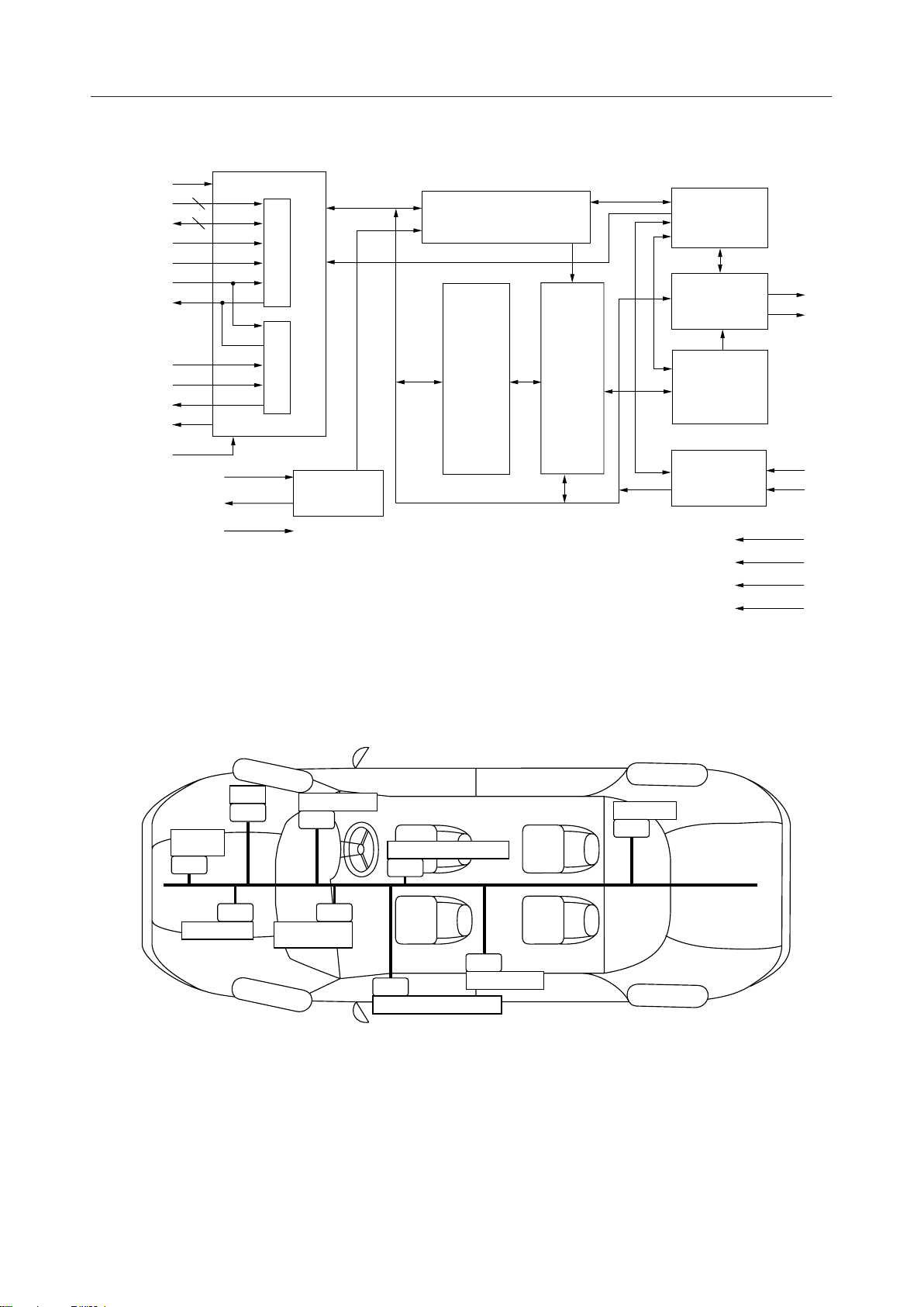
BLOCK DIAGRAM
MSM9225
CS
A7-0
AD7-0/D7-0
PALE
PWR
PRD/SRW
PRDY/SWAIT
SCLK
SDI
SDO
INT
Mode1, 0
8
8
XT
XT
RESET
RD
RDY
RW
WAIT
microcontroller interface
Serial I/F Parallel I/F
Timing
generator
Bit timing logic (BTL)
Data
memory
manege-
Data
ment
logic
Bit stream
logic
(BSL)
Transmission
control logic
(TCL)
Error
management
logic (EML)
Receive
control logic
(RCL)
Tx0
Tx1
Rx0
Rx1
V
DD
GND
AV
DD
AGND
CONFIGURATION EXAMPLE
ABS
CAN
Engine
controller
CAN
CAN
Transmission
Power steering
CAN
CAN
Automatic
air conditioner
Seat-position controller
CAN
CAN
CAN
Outside mirror controller
Power window
Suspention
CAN
CAN Bus
2/73
Page 3
¡ Semiconductor
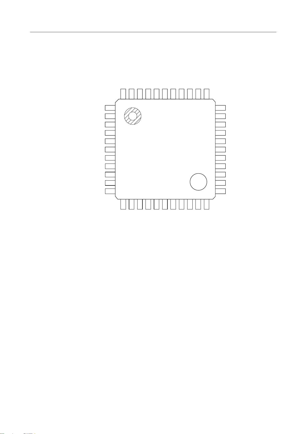
PIN CONFIGURATION (TOP VIEW)
A3
44
A2
43
A1
42
A0
41
DD
V
40
GND
39
AD7/D7
AD6/D6
38
37
AD5/D5
AD4/D4
36
35
MSM9225
AD3/D3
34
A4
A5
A6
A7
SDO
GND
SDI
SCLK
PRD/SRW
CS
INT
10
11
AD2/D2
22
Tx0
33
32
31
30
29
28
27
26
25
24
23
AD1/D1
AD0/D0
Mode1
Mode0
GND
PALE
PWR
RESET
V
DD
Tx1
1
2
3
4
5
6
7
8
9
12
13
14
15
16
17
18
19
20
21
DD
XT
V
XT
GND
Rx0
AGND
Rx1
DD
AV
GND
PRDY/SWAIT
44-Pin Plastic QFP
3/73
Page 4

¡ Semiconductor
PIN DESCRIPTIONS
MSM9225
Symbol Type
CS I
A7-0 I
AD7-0
/D7-0
PWR I
RPD/SRW I
PALE I
SDI I
SDO O
SCLK I
PRDY
/SWAIT
Pin
10
41-44,
1-4
31-38
26
9
27
7
5
8
16
I/O
O
Description
Chip select pin. When "L", PALE, PWR, PRD/SRW, SCLK and SDO pins are valid.
Address bus pins (when using separate buses). If used with a multiplexed bus or if
used in the serial mode, fix these pins at "H" or "L" levels.
Multiplexed bus: Address/data pins
Separate buses: Data pins
If used in the serial mode, fix these pins at "H" or "L" levels.
Write input pin during parallel mode. Data is captured when this pin is at a "L" level.
If used in the serial mode, fix this pin at a "H" or "L" level.
Parallel mode: Read signal pin.
When at a "L" level, data is output from the data pin.
Serial mode: Read/write signal pin.
When at a "H" level, data is output from the SDO pin.
When at a "L" level, the SDO pin is at high impedance, and data is captured beginning
with the second byte of data input from the SDI pin.
Address latch signal pin.
When at a "H" level, addresses are captured.
If used in the parallel mode and the address latch signal is unnecessary or in the
serial mode, fix this pin at a "H" or "L" level.
Serial data input pin.
Addresses (1st byte) and data (beginning from the 2nd byte) are input to this pin,
LSB first. If used in the parallel mode, fix this pin at a "H" or "L" level.
Serial data output pin.
When the CS pin is at a "H" level, this pin is at high impedance. When CS is at a "L"
level, data is output from this pin LSB first.
If used in the parallel mode, fix this pin at a "H" or "L" level.
Shift clock input pin for serial data.
At the rising edge of the shift clock, SDI pin data is captured. At the falling edge, data
is output from the SDO pin.
Ready output pin.
If the microcontroller's bus cycle is fast, a signal is output to extend the bus cycle
until the internal access is completed.
Internal access in progress After completion of access
Parallel mode
Serial mode
"L" level output High impedance output
"H" level output "L" level output
4/73
Page 5

¡ Semiconductor
Symbol Type DescriptionPin
MSM9225
Microcontroller interface select pins.
Mode1, 0 I
29, 30
INT O11
RESET I25
XT I13
XT O14
12, 24,
DD
40
6, 15, 21
28, 39
DD
Mode1
0
0
1
1
Mode0
0
1
0
1
Parallel mode
Serial mode
Separate buses No address latch signal
Multiplexed buses
Interface
With address latch signal
Interrupt request output pin.
When an interrupt request occurs, a "L" level is output.
Three types of interrupts share this pin: transmission complete, reception complete,
and error.
Reset pin.
System is reset when this pin is at a "L" level.
Clock pins. If internal oscillator is used, connect a crystal oscillator. If external
clock is input, input clock via XT pin. The XT pin should be left open.
Receive input pin. Differential amplifier included.RX0, RX1 I18, 19
Transmission output pin.TX0, TX1 O22, 23
—
Internal logic power supply pin.V
Internal logic GND pin.GND —
Power supply pin for receive input differential amplifier.AV
—20
GND pin for receive input differential amplifier.AGND —17
5/73
Page 6

¡ Semiconductor
MSM9225
FUNCTIONAL DESCRIPTION
Data Memory
Before starting communication, messages for communication and various control registers
must be set at the data memory.
Addresses X0hex to XDhex are the message memory, which stores control registers, identifiers
and the contents of each message.
In this address space, the higher 4 bits of an address corresponds to the number of messages,
and a maximum of 16 (0Xhex to FXhex) can be stored. Each message has an area to store a
maximum of 8 bytes of data memory, 1 byte of control register, and a maximum of 5 bytes of
an identifier.
This means that the data memory capacity for messages is: 16 messages ¥ (8 bytes for a message
+ 1 byte for a control register + 5 bytes for an identifier) = 224 bytes.
Addresses XEhex to XFhex are allocated to the control registers.
The configuration of data memory is as follows
Data memory configuration
Address Function
A7 A6 A5 A4 A3 A2 A1 A0 IDFM = 0 (standard) IDFM = 1 (extended)
Message control register
Identifier 0
Identifier 1
— Message 5
— Message 6
— Message 7
number of
messages
0000
1111
Ø
0000
0Corresponds to
001
0010
0011
0100
0101
0110
0111
1000
1001
1010
1011
1100
1101
Message 0 Identifier 2
Message 1 Identifier 3
Message 2 Identifier 4
Message 3 Message 0
Message 4 Message 1
Message 5 Message 2
Message 6 Message 3
Message 7 Message 4
0000
Ø
1111
1110
Various control registers
1111
6/73
Page 7
¡ Semiconductor
MSM9225
Message Memory
The message memory stores messages to be transmitted/received.
For transmission, only messages stored in the message memory can be transmitted. A message
with the highest priority among messages requested for transmission is sent.
For receiving, only messages that have an identifier stored in the message memory can be
received. When a message is received normally, and its identifier matches with the identifier
stored in the message memory, data of the received message is written to the message area of
the corresponding message in the message memory.
The message memory can store a maximum of 16 messages. Set messages at the NMES register.
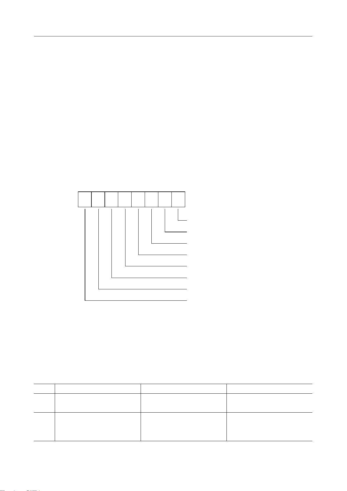
1. Inside message control register (X0hex)
This register performs various controls for a message.
Set this register for each message.
The bit configuration is as follows:
Address MSB
¥ 0h
76543210
LSB
ARES : Automatic transmission
FRM : Message format setting
EIT : Transmission completion interrupt enable
EIR : Receive completion interrupt enable
RCS : Receive status
TRQ : Transmission request
Not used
MMA : Message memory access enable
(1) Message memory access request/enable bit: MMA
This bit prevents contention between the microcontroller and CAN when accessing the
message memory.
When the microcontroller accesses the message memory, "1" is written to the MMA bit
regularly. The microcontroller confirms that the MMA bit is "1", and then accesses the
message memory. Write "0" to the MMA bit when the microcontroller accessing ends.
Operations by the MMA bit are shown in the following table.
At reset, the MMA bit is set to "0".
MMA
0
1
Microcontroller
Accesses from microcontroller
to message memory are disabled
Accesses from microcontroller
to message memory are enabled
Reception
Operate
Reading of received data
Stop
Rewriting of control area
Transmission
Operate
Stop
Rewriting of control area
Rewriting of transmission data
7/73
Page 8

¡ Semiconductor
(2) Transmission request: TRQ
When a message is transmitted, the microcontroller writes "1" to this bit. When
transmission ends normally, CAN writes "0". This means that the TRQ bit is "1" during
transmission. Therefore, to request transmission, confirm that the TRQ bit is "0" first,
then write "1" to the TRQ bit. When the remote frame is received while the ARES bit is
"1", the TRQ bit is set to "1".
At reset, the TRQ bit is set to "0".
(3) Receive status: RCS
When receiving completes, the RCS bit becomes "1". Write "0" to the RCS bit before the
microcontroller calls up receive data. When receiving the remote frame, the RCS bit
becomes "1" just after the reception.
At reset, the RCS bit is set to "0".
(4) Receive completion interrupt enable: EIR
The microcontroller sets interrupt request signal generation disable/enable when
receiving completes.
The EIR bit is valid when the EINTR bit of the CANI register is “1”.
At reset, the EIR bit is set to "0".
MSM9225
(5) Transmission completion interrupt enable: EIT
The microcontroller sets interrupt request signal generation disable/enable when
transmission completes.
The EIT bit is valid when the EINTT bit of the CANI register is “1”.
At reset, the EIT bit is set to "0".
(6) Message format setting: FRM
The microcontroller sets the format of the message to be sent/received. A message in a
format other than the specified format cannot be sent/received.
For the relationship between setting and format, see the table below.
When a message specified to a group message is received, the content of the RTR bit is
written.
At reset, the FRM bit is set to "0".
FRM Message Type Transmission Format Receive Format
0
1
Standard message Data frame Remote frame
Group message Transmission disable Data frame
Standard message
Group message
Remote frame
Transmission disable
Data frame
Remote frame
(7) Automatic transmission : ARES
If the data frame is automatically transmitted after remote frame reception, the ARES bit
should be set to "1".
At reset, the ARES bit is set to "0".
8/73
Page 9
¡ Semiconductor
g
2. Identifier 0 (X1hex)
This register sets the data length code and a part of the identifier.
Set this register for each message.
The bit configuration is as follows:
MSM9225
Address MSB
¥ 1h
76543210
(1) Format setting: IDFM
The microcontroller sets the message format.
At reset, the IDFM bit is undefined.
IDFM Operation
0 Standard format (ID = 11 bits)
Extended format (ID = 29 bits)I
LSB
IDB26 :
IDB27 :
IDB28 :
DLC0 :
DLC1 :
DLC2 :
DLC3 :
IDFM : Format settin
Identifier
Data length code
(2) Data length code: DLC3 to DLC0
This is control field data to set the number of bytes of a data field. 0 to 8 can be set.
At reset, these bits are undefined.
(3) Identifier: IDB28 to IDB26
These bits set the identifier field.
For standard format (IDFM = 0), the higher 3 bits of the 11 bits are set.
For extended format (IDFM = 1), the higher 3 bits (ID28 to ID26) of the 29 bits (ID28 to
ID0) are set.
At reset, these bits are undefined.
9/73
Page 10
¡ Semiconductor
3. Identifier 1 (X2hex)
This register sets the identifier.
Set this register for each message.
The bit configuration is as follows:
MSM9225
Address MSB
¥ 2h
76543210
LSB
IDB18 :
IDB19 :
IDB20 :
IDB21 :
Identifier
IDB22 :
IDB23 :
IDB24 :
IDB25 :
(1) Identifier: IDB25 to IDB18
These bits set the lower 8 bits of the 11 bits of the identifier field.
For standard format (IDFM = 0), the lower 8 bits of the 11 bits are set.
For extended format (IDFM = 1), ID25 to ID18 of the 29 bits (ID28 to ID0) are set.
At reset, these bits are undefined.
4. Address: X3 to XDhex
For standard format (IDFM = 0), addresses X3 to XAhex become the transmission/receive
data storage area.
For extended format (IDFM = 1), addresses X3 to X5hex are used to set the identifier field, and
addresses X6 to XDhex become the transmission/receive data storage area.
For both, a maximum of 8 bytes of transmission/receive data can be stored, but the number
of transmittable/receivable bytes must have been set by data length code.
At reset, message content is undefined.
The relationship between address and identifier bits for extended format (IDFM = 1) is as
follows:
10/73
Page 11
¡ Semiconductor
MSM9225
Adderss MSB
¥ 3h
Address MSB
¥ 4h
LSB
76543210
IDB10 :
IDB11 :
IDB12 :
IDB13 :
Identifier 2
IDB14 :
IDB15 :
IDB16 :
IDB17 :
LSB
76543210
Address MSB
¥ 5h
IDB2 :
IDB3 :
IDB4 :
IDB5 :
Identifier 3
IDB6 :
IDB7 :
IDB8 :
IDB9 :
LSB
76543210
Not used (Don't care)
Not used (Don't care)
Not used (Don't care)
Not used (Don't care)
Not used (Don't care)
Not used (Don't care)
IDB0 :
Identifier 4
IDB1 :
11/73
Page 12

¡ Semiconductor
Control Register
These registers listed below control various operations of CAN.
MSM9225
Address Symbol
0EH CANC
0FH CANI
1EH NMES Number of message specification registers
1FH BTR0 CAN bus timing register 0
2EH BTR1 CAN bus timing register 1
2FH TIOC Communication input/output control register
3EH GMR0 Group message register 0
3FH GMR1 Group message register 1
4EH GMSK00 Message mask register 00
4FH GMSK01 Message mask register 01
5EH GMSK02 Message mask register 02
5FH GMSK03 Message mask register 03
6EH GMSK10 Message mask register 10
6FH GMSK11 Message mask register 11
7EH GMSK12 Message mask register 12
7FH GMSK13 Message mask register 13
8EH STBY Standby control register
8FH Not used (reserve area)
9EH TMN Communication message number register
9FH CANS CAN status register
AEH TEC Transmission error counter
AFH REC Receive error counter
BEH
BFH
CEH
CFH
DEH
DFH
EEH
EFH
FEH
FFH
CAN control register
CAN interrupt control register
Not used (reserve area)
Name
12/73
Page 13

¡ Semiconductor
1. CAN control register (CANC: 0Ehex)
This register controls the operation of CAN.
The bit configuration is as follows:
MSM9225
Address MSB
0Eh
76543210
LSB
INIT : Initialize
TIRS : Transmission identifier retrieval
Not used
SYNC : Bit synchronization
CANA : CAN write flag
T x F : Transmission flag
R x F : Receive flag
Not used
(1) Initialize: INIT
This bit is used to initialize the communication control area. To start initialization, write
"1" to INIT, read INIT and confirm that INIT is "1", then initialize. To end initialization,
write "0" to INIT, read INIT, and confirm that INIT is "0". For both, initialization mode
is not set/cleared until the above procedure is executed.
If the INIT bit is set to "1" during the transmission or receive operation, the initialization
will start after the communication completes.
When the INIT bit is set to "1", the communication operation stops but the error counter
and data memory are held.
To initialize message memory, write the number of messages to be used to the number
of messages setting register, NMES, then write the inside message control register,
identifier 1, and identifier 2 sequentially from message 0 for all messages.
At reset, INIT is set to "1".
(2) Transmission identifier retrieval: TIRS
This bit is used to scan identifiers sequentially from message 0 to the last message of the
message memory, detecting priority of the message for which the transmission request
TRQ is "1" and starting to transmit the messages. TIRS will be set to "0" when there are
no transmission request messages after scanning or transmitting.
At reset, TIRS is set to "0".
(3) Bit synchronization: SYNC
This bit is used to set the bit synchronization edge to synchronize at the CAN bus.
When SYNC is "0", the synchronization edge is set at the falling edge of data.
When SYNC is "1", the synchronization edge is set at both the rising and falling edges of
data.
At reset, SYNC is set to "0".
13/73
Page 14
¡ Semiconductor
p
(4) CAN write flag: CANA
This bit is used to indicate receive data write status to the message memory. CANA is
"1" while CAN is writing receive data to the message memory.
This is a read-only flag.
(5) Transmission flag: TxF
This bit is used to indicate transmission operation status.
When TxF is "0", CAN is in transmission operation stop status.
When TxF is "1", CAN is in transmission operation status. TxF becomes "0" when
transmission completes.
This is a read-only flag.
(6) Receive flag: RxF
This bit is used to indicate receive operation status.
When RxF is "0", CAN is in receive operation stop status.
When RxF is "1", CAN is in receive operation status. RxF becomes "0" when receiving
completes.
This is a read-only flag.
MSM9225
2. CAN interrupt register (CANI: 0Fhex)
This register controls CAN interrupts.
The bit configuration is as follows:
Address MSB
0Fh
76543210
(1) Transmission interrupt output enable: EINTT
This bit is used to output transmission interrupt signal INTT from interrupt pin INT
when transmission completes.
When EINTT is "0", a transmission interrupt signal is not output from the interrupt pin.
When EINTT is "1", a transmission interrupt signal is output from the interrupt pin.
At reset, EINTT is set to "0".
LSB
EINTT : Transmission interrupt output enable
EINTR : Receive interrupt output enable
EINTE : Error interrupt output enable
Not used
ITF : Transmission interrupt request flag
IRF : Receive interrupt request flag
IEF : Error interrupt request flag
MEINT : Master interru
t control enable
(2) Receive interrupt output enable: EINTR
This bit is used to output receive interrupt signal INTR from interrupt pin INT when
reception completes.
When EINTR is "0", a receive interrupt signal is not output from the interrupt pin.
When EINTR is "1", a receive interrupt signal is output from the interrupt pin.
At reset, EINTR is set to "0".
14/73
Page 15
¡ Semiconductor
(3) Error interrupt output enable: EINTE
When an error occurs, this bit is used to output error interrupt signal INTE from interrupt
pin INT.
When EINTE is "0", an error interrupt signal is not output from the interrupt pin.
When EINTE is "1", an error interrupt signal is output from the interrupt pin.
At reset, EINTE is set to "0".
(4) Transmission interrupt request flag: ITF
ITF becomes "1" when a transmission interrupt is generated. Only "0" can be written to
this bit.
At reset, ITF is set to "0".
(5) Receive interrupt request flag: IRF
IRF becomes "1" when a receive interrupt is generated. Only "0" can be written to this bit.
At reset, IRF is set to "0".
(6) Error interrupt request flag: IEF
IEF becomes "1" when an error occurs. Only "0" can be written to this bit.
At reset, IEF is set to "0".
MSM9225
(7) Master interrupt control enable: MEINT
This bit is used to set enable/disable of communication interrupts.
The flowchart of interrupt control is shown below.
When MEINT is "0", interrupt request control is disabled.
When MEINT is "1", interrupt request control is enabled.
At reset, MEINT is set to "0".
MEINT
0
1
0
1
0
1
INT pin
0
1
EINTT
EINTR
EINTE
ITF
Interrupt factor
(transmission completion)
EIT (each message)
IRF
Interrupt factor
(reception completion)
EIR (each message)
IEF
Interrupt factor (An error occurs)
15/73
Page 16
¡ Semiconductor
3. Number of messages specification register (NMES: 1Ehex)
This is a register to set the number of messages to be stored in the message memory.
A maximum of 16 messages can be set, with message numbers 0 to 15.
Writing to NMES is enabled when initialize bit INIT of the CAN control register (CANC:
OEhex) is "1".
At reset, NMES is set to "0000".
The bit configuration and relationship between message number and number of messages
are as follows:
MSM9225
Address MSB
1Eh
***
*
****
****
········
···· · · · ·
****
****
: Don't Care
*
4. CAN bus timing register 0 (BTR0: 1Fhex)
This register sets the baud rate prescaler and synchronization jump width (SJW) used for bus
timing. Writing to the BTR0 bit is enabled, when the INIT bit of the CAN control register
(CANC: 0Ehex) is "1".
The bit configuration is as follows:
Address MSB
1Fh
76543210
NMES3 NMES2 NMES1 NMES0
0000
0000
1110
1111
LSB
LSB
Number of message
1
2
·
·
15
16
BRP0 :
BRP1 :
BRP2 :
BRP3 :
BRP4 :
BRP5 :
SJWA :
SJWB :
Baud rate
prescaler
Synchronization
Jump Width
16/73
Page 17
¡ Semiconductor
(1) Baud rate prescaler: BRP5 to BRP0
This is a 6-bit prescaler to set the BTL cycle time and SJW of the basic clock for
communication operation.
The relationship between the bit content and BTL is as follows:
At reset, BRP5 to BRP0 are set to "000000".
BRP5 BRP3 BRP2 BRP1 BRP0
BRP4
00000
00001
·····
·····
11110
1
0
0
·
·
1
11111
The BTL cycle time is given by the following operation.
BTL cycle time = 2 ¥ (25 ¥ BRP5 + 24 ¥ BRP4 + 23 ¥ BRP3 + 22 ¥ BRP2 + 21 ¥ BRP1 + BRP0
+ 1)/f
OSC
*) System clock is 1/2 division of oscillation frequency.
f
is the oscillation frequency.
OSC
MSM9225
BTL cycle time
1X system clock cycle
2X system clock cycle
·
·
63X system clock cycle
64X system clock cycle
(2) SJW: SJWA, SJWB
This is a 2-bit register to set SJW.
The relationship between bit content and SJW is as follows:
At reset, SJWA and SJWB are set to “00”.
SJWB SJWA SJW1, SJW2
001 ¥ BTL cycle
012 ¥ BTL cycle
103 ¥ BTL cycle
114 ¥ BTL cycle
17/73
Page 18
¡ Semiconductor
MSM9225
5. CAN bus timing register 1 (BTR1: 2Ehex)
This register sets the sampling count, sampling point and transmit point used for bus timing.
Writing to the BTR1 bit is enabled, when the INIT bit of the CAN control register (CANC:
0Ehex) is "1".
The bit configuration is as follows:
Address MSB
2Eh
76543210
LSB
(1) Time segment 1: TSEG13 to TSEG10
This is a 4-bit register to set the sampling point.
The relationship between bit content and TSEG1 is as follows:
At reset, TSEG13 to TSEG10 are set to "0000".
TSEG10 :
TSEG11 :
TSEG12 :
TSEG13 :
TSEG20 :
TSEG21 :
TSEG22 :
Not used :
Time
segment 1
Time
segment 2
TSEG13 TSEG12 TSEG11 TSEG10 TSEG1
0000
0001
····
····
1110
1111
1 ¥ BTL cycle
2 ¥ BTL cycle
·
·
15 ¥ BTL cycle
16 ¥ BTL cycle
(2) Time segment 2: TSEG22 to TSEG20
This is a 3-bit register to set the transmit point.
The relationship between the bit content and TSEG2 is as follows:
At reset, TSEG22 to TSEG20 are set to "000".
TSEG22 TSEG21 TSEG20 TSEG2
000
001
···
···
110
111
1 ¥ BTL cycle
2 ¥ BTL cycle
·
·
7 ¥ BTL cycle
8 ¥ BTL cycle
18/73
Page 19
¡ Semiconductor
(3) Bit timing
Bit timing is set by CAN bus timing registers 0 and 1. The relationship between 1 bit time
of a message and a CAN bus timing (the MSM9225 register) is as follows:
MSM9225
1 bit time
PROP-SEGSYNC-SEG PHASE-SEG1 PHASE-SEG2
SJW1
(BTR0 : SJWB/A)
1BTL
cycle
If setting is :
BTR0 = "01000001" ...SJWB = "0" SJWA = "1" BRP5-0 = "000001"
BTR1 = "00000001"...TSEG2 = "000" TSEG1 = "0001"
then the bit timing is as follows
Sync segment 1 BTL cycle (fixed)
SJW 1 2 BTL cycle
TSEG 1 2 BTL cycle
TSEG 2 1 BTL cycle
SJW 2 2 BTL cycle
1 bit time 8 BTL cycle
TSEG1
(BTR1 : TSEG13-10)
Sampling
TSEG2
(BTR1 : TSEG22-20)
point
SJW2
(= SJW1)
Sampling point = 5 BTL cycle
If f
= 16 MHz, then 1 BTL cycle is :
osc
BTL cycle = 2 ¥ (25 ¥ 0 + 24 ¥ 0 + 23 ¥ 0 + 22 ¥ 0 + 21 ¥ 0 + 1 + 1) / 16 MHz = 0.25 ms
Therefore 1 bit time is :
8 BTL cycle = 8 ¥ 0.25 ms = 2.0 ms
(= 500 Kb/s)
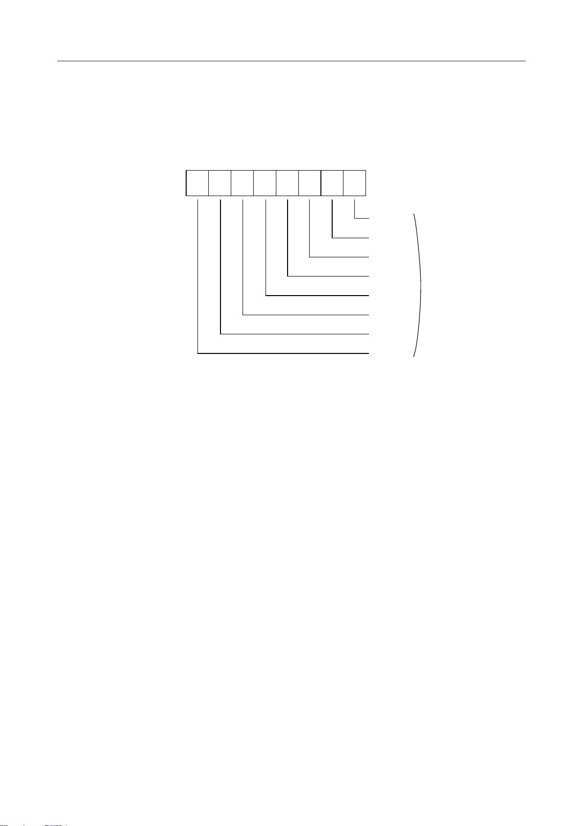
6. Communication input/output control register (TIOC: 2Fhex)
This register sets the communication mode and output buffer format.
Writing to the TIOC bit is enabled, when the INIT bit of the CAN control register (CANC:
0Ehex) is "1".
The bit configuration is as follows:
19/73
Page 20
¡ Semiconductor
MSM9225
Address MSB
2Fh
76543210
LSB
OCMD0
OCMD1
OCPOL0
OCTN0
OCTP0
OCPOL1
OCTN1
OCTP1
:
Output mode
:
:
:
buffer format
:
:
:
buffer format
:
Tx0 output
Tx1 output
(1) Time segment 1: OCMD1 to OCMD0
These bits are used to set the output mode of output pins Tx0 and Tx1.
The relationship between the bit content and output mode is as follows:
At reset, OCMD1 to OCMD0 are set to “00”.
setting
OCMD1 OCMD0
00
01
10
11
Output mode of Tx0 and Tx1
[Double layer mode]
Transmission data "0" is output from Tx0 and Tx1 altermately.
Output example
Data
Tx0
Tx1
[Disabled]
[Single layer mode]
Same bit string data is output from both Tx0 qnd Tx1.
Output example
Data
Tx0
Tx1
[Clock output mode]
Bit string data is output from Tx0.
Synchrinization clock is output from Tx1.
Output example
Data
101010
101010
101010
Tx0
Tx1
20/73
Page 21
¡ Semiconductor
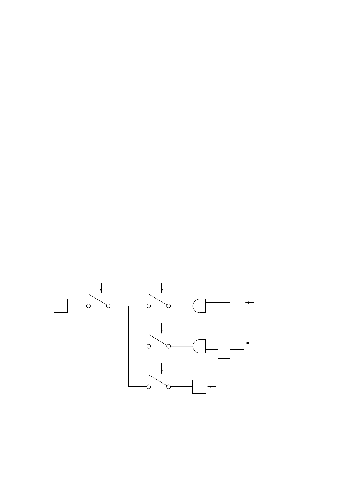
(2) Output driver format setting: OCPOL, OCTN, OCTP
OCPOL is used to set the polarity of output.
OCTN is used to set the open/drain mode of the Nch transistor of the output driver.
OCTP is used to set the open/drain mode of the Pch transistor of the output driver.
The circuit configuration of the output driver and the relationship between bit content
and output driver format are as follows:
At reset, all bits are set to "0".
MSM9225
Output data
Synchronization
clock
Circuit configuration
Output control
circuit
V
DD
P
ch
N
ch
GND
V
DD
P
ch
N
ch
GND
Tx0
Tx1
21/73
Page 22

¡ Semiconductor
Mode OCTP OCTN OCPOL Output data Pch Tr Nch Tr Tx pin output level
Floating
Pulldown
Pullup
Push-pull
Output driver format
0 0 0 0 off off
0 0 0 1 off off
0 0 1 0 off off
0 0 1 1 off off
0 1 0 0 off on
0 1 0 1 off off
0 1 1 0 off off
0 1 1 1 off on
1 0 0 0 off off
100 1 onoff
101 0 onoff
1 0 1 1 off off
1 1 0 0 off on
110 1 onoff
111 0 onoff
1 1 1 1 off on
MSM9225
Floating
Floating
Floating
Floating
"0"
Floating
Floating
"0"
Floating
"1"
"1"
Floating
"0"
"1"
"1"
"0"
22/73
Page 23

¡ Semiconductor
MSM9225
7. Group message register (GMR0: 3Ehex, GMR1: 3Fhex)
These are registers to set the group message mode.
Two messages can be set to the group message mode.
At reset, all bits are set to "0".
The group message mode is valid when the EGM0/EGM1 bit is "1".
Using GMR03 to GMR00 and GMR13 to GMR10, set the message numbers of messages that
are to be set to the group message mode.
The bit configuration is as follows:
Address MSB
3Eh
3Fh
EGM0
EGM1 0 0 0 GMR11 GMR12 GMR11 GMR10
0 0 0 GMR03 GMR02 GMR01 GMR00
LSB
8. Group message mask register (GMSK)
This is a register to judge identifiers when a message with a message number specified by the
group message mode GMR is received.
Using MiID28 to MiID0, set the bits to mask the identifier of a message set by the GMR bit.
Setting "1" masks the bit, setting "0" does not mask the bit.
(M0ID28 to M0ID0 are for GMR0, and M1ID28 to M1ID0 are for GMR1.)
At reset, all bits are set to "0".
The bit configuration is as follows:
Address MSB
4Eh
4Fh
M0ID28
M0ID20 M0ID19 M0ID18 M0ID17 M0ID16 M0ID15 M0ID14 M0ID13
M0ID27 M0ID26 M0ID25 M0ID24 M0ID23 M0ID22 M0ID21
LSB
GMR0
GMR1
GMSK00
GMSK01
5Eh
5Fh
Address MSB
6Eh
6Fh
7Eh
7Fh
M0ID12
M0ID4 M0ID3 M0ID2 M0ID1 M0ID0 0 0 0
M1ID28
M1ID20 M1ID19 M1ID18 M1ID17 M1ID16 M1ID15 M1ID14 M1ID13
M1ID12
M1ID4 M1ID3 M1ID2 M1ID1 M1ID0 0 0 0
M0ID11 M0ID10 M0ID9 M0ID8 M0ID7 M0ID6 M0ID5
LSB
M1ID27 M1ID26 M1ID25 M1ID24 M1ID23 M1ID22 M1ID21
M1ID11 M1ID10 M1ID9 M1ID8 M1ID7 M1ID6 M1ID5
GMSK02
GMSK03
GMSK10
GMSK11
GMSK12
GMSK13
23/73
Page 24

¡ Semiconductor
9. Standby control register (STBY: 8Ehex)
This register sets various modes, such as stop mode.
The bit configuration is as follows:
MSM9225
Address MSB
8Eh
76543210
LSB
STOP : Stop mode
SLEEP : Sleep mode
Not used
Not used
Not used
Not used
Not used
Not used
(1) Stop mode: STOP
If STOP is set to "1", the MSM9225 will enter the stop mode when the CAN bus is idle.
In stop mode, the content of data memory is held but the oscillator and all circuits stop
to save power consumption. Access to/from external units is therefore disabled.
Stop mode is cleared by a reset signal input from the RESET pin or CS pin = "0".
At reset, STOP is set to "0".
(2) Sleep mode: SLEEP
If SLEEP is set to "1", the MSM9225 will enter the sleep mode when the CAN bus is idle.
In sleep mode, the content of data memory is held and the differential input of Rx0 and
Rx1 operates, but the oscillator and other circuits stop operation. Access to/from
external units is therefore disabled.
Sleep mode is cleared by a reset signal input from the RESET pin or CS pin = "0", or by
the differential input of Rx0 and Rx1.
When both stop mode and sleep mode are set at the same time, the MSM9225 enters stop
mode.
At reset, SLEEP is set to "0".
24/73
Page 25

¡ Semiconductor
10. Communication message number register (TMN: 9Ehex)
The communication message number is recorded in this register.
The bit configuration is as follows:
MSM9225
Address MSB
9Eh
76543210
LSB
TRSN0 :
TRSN1 :
TRSN2 :
TRSN3 :
Not used
Not used
Not used
Not used
Transmission
message number
register
(1) Transmission message number register: TRSN3 to TRSN0
This is a register to store the message number when a message is transmitted/received.
When transmission completes, the transmitted message number is stored. When
receiving completes, the received message number is stored. And when an error occurs,
the message number of the message being transmitted/received at that time is stored.
This is a read-only register and is set to "0000" at reset.
25/73
Page 26

¡ Semiconductor
MSM9225
11. CAN status register (CANS: 9Fhex)
This is a status register to indicate the status of CAN.
Bit6 to bit4 are flags for the transmitter and bit1 and bit0 are for the receiver, and this register
is read only.
The bit configuration is shown below.
Address MSB
9Fh
76543210
LSB
REW : Receiver Error Warning
REP : Receiver Error Passive
Not used
Not used
TEW : Transmitter Error Warning
TEP : Transmitter Error Passive
BOFF : Bus OFF flag
Not used
(1) Receiver Error Warning: REW
When the Receiver Error Counter (REC) ≥ 96, REW becomes "1". If REW = "1", the bus
may be seriously damaged. The bus must be tested for this condition.
At reset or when REC < 96, REW becomes "0".
(2) Receiver Error Passive: REP
When the Receive Error Counter (REC) ≥ 128, REP becomes "1".
At reset or when REC < 128, REP becomes "0" (error active)
(3) Transmitter Error Warning: TEW
When the Transmit Error Counter (TEC) ≥ 96, TEW becomes "1".
If TEW = "1", the bus may be seriously damaged. The bus must be tested for this
condition.
At reset or when TEC < 96, TEW becomes "0".
(4) Transmitter Error Passive: TEP
When the Transmit Error Counter (TEC) > 128, TEP becomes "1".
At reset or when TEP < 128, TEP becomes "0".
(5) Bus OFF: BOFF
This flag indicates the CAN bus status.
When the Transmit Error Counter (TEC) > 256 BOFF becomes "1" and the CAN bus is in
the BUS OFF state.
At reset or when TEP < 256, BOFF becomes "0".
26/73
Page 27

¡ Semiconductor
p
12. Transmit Error Counter (TEC: AEhex)
TEC indicates the lower 8 bits of the 9-bit Transmit Error Counter.
The bit configuration is shown below.
MSM9225
Address MSB
AEh
76543210
LSB
TEC0 :
TEC1 :
TEC2 :
TEC3 :
Transmit Error Counter
TEC4 :
TEC5 :
TEC6 :
TEC7 :
At reset, TEC is set to "0000 0000".
The relation between the Transmit Error Counter and TEC is shown below.
Transmit Error
Counter
76543210
8
BOFF (CANS: bit6)
1: Bus off state
TEC (AEh)
TEP (CANS: bit5)
0: Error active state
1: Error
assive state
27/73
Page 28

¡ Semiconductor
p
13. Receive Error Counter (REC: AFhex)
The Receive Error Counter is read-only.
The bit configuration is shown below.
MSM9225
Address MSB
AFh
76543210
LSB
REC0 :
REC1 :
REC2 :
REC3 :
Receive Error Counter
REC4 :
REC5 :
REC6 :
REC7 :
At reset, REC is set to "0000 0000".
The relation between the Receive Error Counter and each register is shown below.
Receive Error
Counter
REC (AFh)
76543210
REP (CANS: bit1)
0: Error active state
1: Error
assive state
28/73
Page 29

¡ Semiconductor
MSM9225
OPERATIONAL DESCRIPTION
MSM9225 operation is described below.
Operational Procedure
Procedures to set and operate various communication protocols are indicated below.
1. Initial setting
The initial setting procedure is indicated below.
Start initial setting
Set INIT bit of CANC register
(0Ehex) to "1"
Read INIT bit
INIT = 1?
YES
Set the number of messages with
the NMES register (1Ehex)
Set the inside message
control register (X0hex)
Set the message unit
(FRM/DCL3-DCL0, /ID28-ID0)
All message
settings complete?
*) Since the INIT bit cannot be set to "1" during
transmission or reception, read and verify its value.
NO
CAN bus timing settings
BTR0 (1Fhex)
BTR1 (2Ehex)
Set Tx0, Tx1, Rx0, Rx1 states
with the TIOC register (2Fhex)
Group message settings
(GMR/GMSK)
NO
YES
Set the interrupt control with the
CANI register (0Fhex)
Set INIT bit of the CANC register
(0Ehex) to "0".
Initial setting complete
29/73
Page 30

¡ Semiconductor
2. Transmit Procedure
The transmit procedure is indicated below.
Start transmit setting
Set TIRS bit of CANC register
(0Ehex) to "0"
Set MMA bit of the inside message
control register (X0hex) to "1"
Read MMA bit
MSM9225
MMA = 1?
YES
Write message data to data memory
Set inside message control
register's MMA = 0 and TRQ = 1
All transmit message
settings complete?
YES
Set TIRS bit of CANC register
(0Ehex) to "1"
NO
*) Since the MMA bit cannot be set to
"1" while the message is being accessed,
read and verify its value.
NO
Transmit setting complete
Transmission operation
30/73
Page 31

¡ Semiconductor
3. Receive Procedure
The receive procedure is indicated below.
Receive procedure
MSM9225
(MSM9225)
Interrupt signal is generated when
reception is complete
INT: 1 Æ 0
Verify that IRF bit of CANI register
(0Fhex) is "1"
Set IRF bit of CANI register
(0Fhex) to "0"
Verify reception message number
with TMN register (9Ehex)
Set RCS bit of inside message
control register (X0hex) to "0"
Read reception data from
data memory
*) Verify that the interrupt is caused by the
reception completion.
NO
Inside message
control register's
RCS = 0?
YES
CANC register's (0Ehex)
CANA = 0?
YES
Receive complete
NO
*) Check whether new reception data has
been written to the same message while data
was being read.
*) Check whether reception data has been written
to another message while data was being read.
This step may be omitted and evaluation performed
based on the interrupt signal.
31/73
Page 32

¡ Semiconductor
MSM9225
4. Message unit rewrites during operation
The procedure to rewrite the IDentifier (ID) and Data Length Code (DLC) during operation
is indicated below. The number of messages set in the NMES register at the initial setting is
the number of (valid) messages that may be rewritten.
Start rewrite
Set MMA bit of inside message
control register (X0hex) to "1"
Read MMA bit
MMA = 1?
YES
Rewrite message unit
FRM/DLC3-DLC0/ID28-ID0
Set MMA bit of inside message
control register to "0"
All message
settings complete?
YES
Rewrite complete
NO
NO
32/73
Page 33

¡ Semiconductor
MSM9225
5. Remote Frame Operation
The following two methods are available for transmission after remote frame reception.
(1) Automatically transmit message data that has been previously set
(2) Set message data and then transmit
5-1. Automatic response
After remote frame reception, this method automatically transmits previously set message
data.
Settings of the inside message control register are listed in the table below.
Bit Symbol Value Comments
5 TRQ 0*
3 EIR —
2 EIT 1
1 FRM 0
Inside message
control register
0 ARES 1
When reception is complete, TRQ bit changes from 0 Æ 1
Set transmit interrupt to verify the end of transmission.
Set the remote frame.
Set automatic response.
A flow chart of the operation is shown on the following page.
33/73
Page 34

¡ Semiconductor
Microcontroller (user) operation MSM9225 operation
Set MMA bit of inside message
MSM9225
Start automatic response
control register (X0hex) to "1"
Read MMA bit
Transmit data
setting
Remote reception
and transmission
MMA = 1?
NO
YES
Set the inside message data register
(X0hex) as shown in previous table
Write transmit data to data memory
Set MMA bit to "0"
Remote frame reception?
NO
YES
Data frame transmission
Remote transmission
verification
Transmission completion generates
interrupt
INT: 1 Æ 0
Verify that ITF bit of CANC
register (0Fhex) is "1"
Set ITF bit to "0"
Set RSC bit of inside message
control register to "0"
Figure: Automatic Response Operation Flow Chart
34/73
Page 35

¡ Semiconductor
MSM9225
5-2. Manual response
In this method, after remote frame reception, the transmit data is set and then transmission
begins.
Settings of the inside message control register are listed in the table below.
Bit Symbol Value Comments
5 TRQ 0
3 EIR 1
2 EIT 1
1 FRM 0
Inside message
control register
0 ARES 0
Set to receive message.
Set interrupt to verify (remote frame) reception.
Set interrupt to verify the end of transmission.
Set the remote frame.
Specify that there will be no automatic response.
A flow chart of the operation is shown on the following page.
The basic operation is a combination of receive and transmit procedures.
35/73
Page 36

¡ Semiconductor
Microcontroller (user) operation MSM9225 operation
MSM9225
Start Manual response
Remote reception
Transmit data setting
Verify reception interrupt
with CANI retgister (0Fhex)
Verify receive message number
with TMN retgister (9Ehex)
Set RCS bit of inside message
control register (X0hex) to "0"
Set MMA bit of inside message
control register to "1"
MMA = 1?
NO
Remote frame reception?
YES
Message reception generates
interrupt
INT: 1 Æ 0
NO
Remote transmission
YES
Write transmit data to data memory
Set inside message control
registers MMA = 0 and TRQ = 1
Set TIRS bit of CANC register
(0Ehex) to "1"
Data frame transmission
Transmission completion generates
interrupt
INT: 1 Æ 0
Verify transmission is complete
Figure: Manual Response Operation Flow Chart
36/73
Page 37

¡ Semiconductor
p
MSM9225
Operation at Receiving Message
1. Priority of message
A message has the priority determined by the identifier setting. To determine priority,
identifiers of messages are compared from the higher bit, and the identifier (set to "0") detected
first has the higher priority. (see the example below)
Identifier (example)
0 01 10101
00 1
0 01 10101
00 0
0 00000101
10
0 00101101
01
In this exam
Priority
Second
First
Fourth
Third
le, priority is determined at the shaded bits.
2. Data length code
When the received data length code (hereafter DLC) matches the DLC being set to the message
memory, the number of bytes of data indicated by the received DLC is received and written to
the message memory. When the received DLC does not match with the DLC being set to
message memory, the MSM9225 operates as follows:
(1) Received DLC > DLC on message memory
The number of bytes of data indicated by the DLC on the message memory is received
and written to the message memory.
The data exceeding the number of bytes indicated by DLC on the memory is not written
to message memory.
(2) DLC on message memory > received DLC
The number of bytes of data indicated by the received DLC is received and written to the
message memory.
3. Group message function
If the group message function is used, a part of an identifier can be masked. This can increase
the number of receivable identifiers.
To use the group message function, set the message number of the target message to set the
group message function at the GMR register. Then set the bits to be masked at the GMSK
register. Depending on the location of bits to be masked, an another identifier being set at the
message memory may be received.
In this case, the priority of identifiers being set on the message memory is calculated and the
identifier having the highest priority is received. The received data is written to the message
memory indicated by the message for which the identifier with the highest priority is set.
37/73
Page 38

¡ Semiconductor
MSM9225
When same identifiers are set to multiple messages on message memory
When same identifiers are set to multiple messages on the message memory, operations are as
follows.
1. Transmit operation
Messages are transmitted sequentially from the smaller message number.
2. Receive operation
The message is always written to the smallest message number.
For example, the same identifier is set at message numbers 1 to 4, as shown below.
Message
number
0
1
2
3
4
5
6
Identifier (example)
0 01 11111
00 1
11 1
1 00 11001
11
1 00111001
11
1 00111001
1 0011100111
0 0000011100
0 0000001110
The range in which the same
identifier is set.
• Transmit operation
If every message above is a transmit message, messages are transmitted sequentially in the
order of message number 5 Æ 0 Æ 6 Æ 1 Æ 2 Æ 3 Æ 4.
• Receive operation
When the identifier "11100111001" is received from the CAN bus, received data is always
written to the message memory which is indicated by the message number 1.
38/73
Page 39

¡ Semiconductor
MSM9225
MICROCONTROLLER INTERFACE
There are basically two methods of interfacing to the microcontroller.
(1) Synchronous serial interface (serial mode)
(2) Parallel bus interface (parallel mode)
Each interface is selected with the Mode0 and Mode1 pins. Refer to the section, PIN
DESCRIPTIONS, "PIN DESCRIPTIONS" for the relation between pin values and interface
selection.
Serial Interface
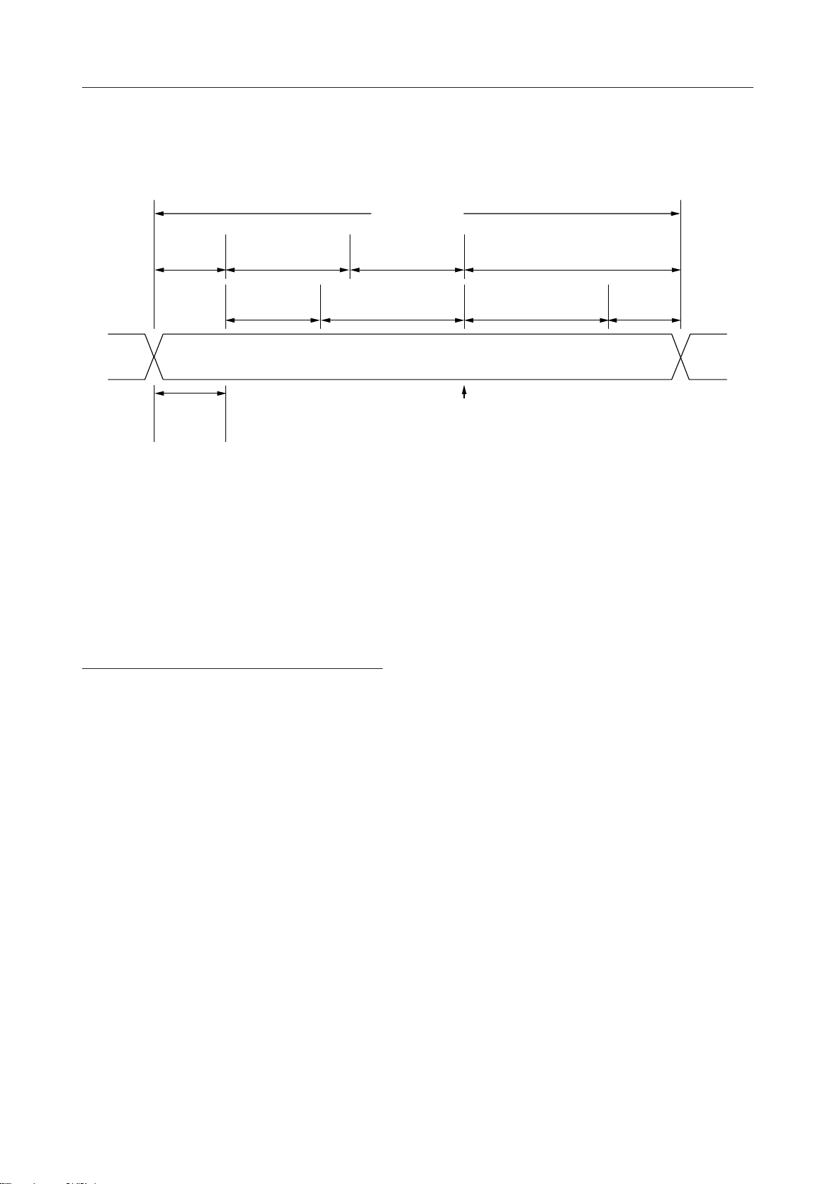
The transfer timing is indicated in the figure.
Address/data transfers begin when the CS pin is at a "L" level and end when it changes to a "H"
level. Because the MSM9225 has an address increment function, the basic transfer consists of "1
address + multiple data." Therefore, to access a nonconsecutive address, the CS must be first
pulled to a "H" level, and then the address reset.
Perform address/data transfers LSB first, in 8-byte units. During a transfer, an interval (WAIT)
is necessary between address and data and between consecutive data transfers. (Refer to the
section, ELECTRICAL CHARACTERISTICS, for interval values.) Note that the WAIT signal is
only generated during the interval between address and data transfers.
(1) Data write
Data write operations are performed with the follwing procedure.
After setting the CS pin and PRD/SRW pin to "L" levels, input an address to the SDI pin.
Synchronized to the rising edge of synchronous clock SCLK, the MSM9225 captures the address
in an internal register. When 8 SCLK clocks are received, the MSM9225 loads the address into
the internal address counter and waits for data reception.
Next, input data to the SDI pin. An internal register captures data in a similar manner to the
address capture, at the rising edge of SCLK. When 8 bits of data have been captured, the
MSM9225 writes the data to the internal memory or register specified by the address that was
received previously, and then increments the counter by 1. If data is to be written to consecutive
addresses, continue the data transfer. After all data has been transferred, set the CS pin to a "H"
level.
(2) Data read
Data read operations are performed with the following procedure.
After setting the CS pin to a "L" level and the PRD SRW pin to a "H" level, in the same manner
as for the data write operation, input an address to the SDI pin. When 8 SCLK clocks are received,
the MSM9225 loads the address into the internal address counter, reads data from the internal
memory or register specified by the address, latches data into a shift register for data output and
increments the address counter. Then, when SCLK is input, latched data is output from the SDO
pin synchronized to the falling edge of SCLK. At this time, the contents of the data input from
the SDI pin does not matter. If there exists remaining data to be read, input another 8 SCLK
clocks. After all the data (at consecutive addresses) has been read, set the CS pin to a "H" level.
If the count value overflows (exceeds XFh), without changing the upper 4 bits of the address, the
address increment function will reset the count value of the lower 4 bits to 0, and will continue
counting.
39/73
Page 40

¡ Semiconductor
MSM9225
40/73
A0 A1 A2 A3 A4 A5 A6 A7 D0 D1 D2 D3 D4 D5 D6 D7 D0 D1 D2 D3 D4 D5 D6 D7SDI
SCLK
CS
SDO
R/W
WAIT
Address reception
Internal
processing
interval
Data reception
Internal processing
interval
Data reception
(Data write &
address + 1)
Internal processing
interval
(Data write &
address + 1)
A0 A1 A2 A3 A4 A5 A6 A7 * * * * * * * * * * * * * * * *SDI
SCLK
CS
R/W
WAIT
Address reception Data transmission
Internal processing
interval
Data transmission
(Data read &
address +1 )
Internal processing
interval
(Data read &
address + 1)
(HiZ)
* * * * * * * * D0 D1 D2 D3 D4 D5 D6 D7 D0 D1 D2 D3 D4 D5 D6 D7SDO
Internal processing
interval
(Data read &
address + 1)
*: Don't Care
(1) Data write timing
(2) Data read timing
Figure: Serial Interface Transfer Timing
Page 41

¡ Semiconductor
Parallel Interface
The following three types of parallel interfaces are available.
(1) Address/data separate bus type, no address latch signal
(2) Address/data separate bus type, with address latch signal
(3) Multiplexed bus type
For transfer timings, refer to the timing diagrams for electrical characteristics.
MSM9225
41/73
Page 42

¡ Semiconductor
MSM9225 CONNECTION EXAMPLES
Microcontroller Interface
(1) Address/data separate bus (no address latch signal)
+5 V
MSM9225Microcontroller
100 kW
INT
CS
RD
WR
WAIT
A7-0
D7-0
RESET
10 kW
4-1, 44-41
38-31
11
INT
10
CS
27
PALE
9
PRD/SRW
26
PWR
16
PRDY/SWAIT
A7-0
AD7-0/D7-0
5
SDO
7
SDI
8
SCLK
25
RESET
XT
XT
Mode1
Mode0
CST16MXW040
13
14
If the clock is supplied
externally,in the same
30
29
manner as for the serial
interface, input the clock
to the XT pin and leave
the XT pin open.
MSM9225
Reset signal
(2) Address/data separate bus (with address latch signal)
+5 V
MSM9225Microcontroller
100 kW
INT
CS
ALE
RD
WR
WAIT
A7-0
D7-0
RESET
10 kW
4-1, 44-41
38-31
11
INT
10
CS
27
PALE
9
PRD/SRW
26
PWR
16
PRDY/SWAIT
A7-0
AD7-0/D7-0
5
SDO
7
SDI
8
SCLK Mode1
25
RESET Mode0
XT
XT
CST16MXW040
13
14
30
29
Reset signal
42/73
Page 43

¡ Semiconductor
(3) Address/data multiplexed bus
100 kW
INT
CS
ALE
RD
WR
WAIT
AD7-0
RESET
+5 V
10 kW
4-1, 44-41
38-31
MSM9225Microcontroller
11
INT
10
CS
27
PALE
9
PRD/SRW
26
PWR
16
PRDY/SWAIT
A7-0
AD7-0/D7-0
5
SDO
7
SDI
8
SCLK Mode1
25
RESET Mode0
XT
XT
CST16MXW040
13
14
30
29
MSM9225
Reset signal
(4) Serial interface
WAIT
SDIN
SDOUT
SCLK
RESET
INT
CS
ALE
RD
WR
100 kW
+5 V
10 kW
4-1, 44-41
38-31
MSM9225Microcontroller
11
INT
10
CS
27
PALE
9
PRD/SRW
26
PWR
16
PRDY/SWAIT
A7-0
AD7-0/D7-0
5
SDO
7
SDI
8
SCLK Mode1
25
RESET Mode0
XT
XT
If self-excitation is used,
in the same manner as for
the separate bus, connect
an external oscillator.
13
14
Open
30
29
Reset signal
CLK
43/73
Page 44

¡ Semiconductor
CAN Bus Interface
(1) Electrically isolated from bus transceiver (PCA82C250)
MSM9225
MSM9225
Rx1
Rx0
Tx1
Tx0
19
18
23
22
Open
8
7
5
3
2
1
4
6
+5 V
0.1 mF
Open
Open
390 W
390 W
PCA82C250
4
RxD
1
TxD
V
CC
GND
CANH
CANL
Vref
Rs
3
2
7
6
5
8
124 W
0.1 mF
CAN BUS LINE
Open
124 W
470 kW
6N137
2
0.1 mF
390 W
390 W
Open
Open
1
4
6
8
7
5
3
V
CC
E
GND
6N137
ANODE
O.P.CATH
6.8 kW3.6 kW
(2) Directly connected to bus transceiver (PCA82C250)
MSM9225
19
Rx1
18
Rx0
23
Tx1
Open
22
Tx0
PCA82C250
5
Vref
4
RxD
1
TxD
V
CC
GND
CANH
CANL
124 W
3
0.1 mF
2
7
6
CAN BUS LINE
From microcontroller (port pin)
(Normal "L" output)
470 kW
8
Rs
124 W
44/73
Page 45

¡ Semiconductor
(3) Monitoring the CAN bus
Battery
MSM9225
MSM9225
Microcontroller
+5 V
Rx1
Rx0
Tx1
Tx0
Port
Port
Port
19
18
23
22
Open
10
13
1
3
2
5
4
6
V
CC
GND
INH
RxD
TxD
STB
NERR
EN
14
BAT
7
PCA82C252
WAKE
RTH
CANH
CANL
RTL
8
11
12
9
CAN BUS LINE
45/73
Page 46

¡ Semiconductor
MSM9225
PROTOCOL
The CAN (Controller Area Network) is a high-speed multiplexed communication protocol
designed to perform real-time communication inside an automobile. CAN specifications are
broadly classified into two layers, the physical layer and the data link layer. The data link layer
consists of logical link control and medium access control.
The configuration of each layer is listed below.
Upper
Lower
Application layer (not including object)
Data link layer
• Logical link control (LLC): message and status handling
• Medium access control (MAC): as per protocol
Physical layer: signal level and bit representation
Protocol Mode Function
(1) Standard format mode
2032 types of identifiers can be set in this mode.
Since the identifier is 11 bits, 2032 types of messages can be handled.
(2) Extended format mode
2032 ¥ 218 types of identifiers can be set in this mode.
In the standard format mode, the identifier is 11 bits. However, in the extended format mode,
the identifier is extended to 29 bits (11 + 18).
If the SRR and IDE bits of the arbitration field are both "recessive", the mode changes to the
extended format mode.
If remote frames for an extended format mode message and a standard format message are
transmit simultaneously, the node that transmit the extended format message will change to
the receive state.
Message Format
CAN protocol messages have the following 4 types of frames.
(1) Data frame : transmit data frame
(2) Remote frame : transmit request frame from the receive side
(3) Error frame : frame that is output when an error is detected
(4) Overload frame : frame that is output when the receive side has not completed preparing
for reception
* In a wired-OR logic circuit, the stronger value is defined as "dominant" and the weaker value
as "recessive". In figures hereafter, dominant (abbreviation: D) = 0, and recessive (abbreviation:
R) = 1.
46/73
Page 47

¡ Semiconductor
1. Data frame and remote frame
(1) Data frame
The data frame is for data transmission and consists of 8 fields.
Data frame
R
D
12 3 4 5 678
MSM9225
Interframe space
End-of-frame
Ack field
CRC field
Data field
Control field
Arbitration field
Start-of-frame
(2) Remote frame
This frame is transmit when the receive node requests transmission.
The data field is deleted from the data frame and the RTR bit of the arbitration field is made
"recessive".
Remote frame
R
D
12 3 5 678
Interframe space
End-of-frame
Ack field
CRC field
Control field
Arbitration field
Start-of-frame
* Even when the data length code of the control field is nonzero, there will be no data frame
transfer.
47/73
Page 48

¡ Semiconductor
(
)
(
)
(
)
(
)
(
)
MSM9225
(3) Description of each frame
(a) Start-of-frame
Start-of-frame indicates the beginning of a data frame or remote frame and is one dominant
bit.
(Interframe space
or bus idle)
R
D
Start-of-frame
1 bit
(Arbitration field)
The start-of-frame begins when the bus line level changes.
If "dominant" is detected at the sample point, reception continues.
If "recessive" is detected at the sample point, the bus becomes idle.
(b) Arbitration field
This field sets priority and data frame/remote frame protocol modes.
The arbitration field consists of an identifier, RTR bit, and extended format setting bits.
Standard format mode
Arbitration field
R
D
ID28 ID18
Extended format mode
Identifier
(11 bits)
RTR
1 bit
(Control field)
IDE
(r1)
1 bit
r0
Arbitration field
R
D
ID28 ID18
Identifier
(11 bits)
SRR
1 bit
IDE
ID17 ID0
1 bit
* Notes:
ID28 to ID0 is the identifier.
The identifier is transmitted MSB first.
It is prohibited to set the identifier = 1111111XXXXX.
Identifier
(18 bits)
RTR
1 bit
(Control field)
r1 r0
48/73
Page 49

¡ Semiconductor
(
)
MSM9225
Number of Identifier Bits
Protocol mode
Standard format mode
Extended format mode
No. of bits
11 bits
29 bits
RTR Bit Setting
RTR bit
Dominant
Recessive
Frame type
Data frame
Remote frame
Mode Setting
Protocol mode
Standard format mode
Extended format mode
SRR bit
None
Recessive
IDE bit
Dominant
Recessive
(c) Control field
The control field sets the number of data bytes (N) in the data field. (N: 0 to 8)
r1 and r0 are fixed as "dominant". The number of bytes is set with DLC3 to DLC0.
(Arbitration field)
R
D
RTR r0 DLC3
r1
IDE
Control field
DLC2
(Data field)
DLC1 DLC0
During the standard format mode, the r1 bit and IDE bit of the arbitration field are the same bit.
49/73
Page 50

¡ Semiconductor
(
)
(
)
(
)
MSM9225
Data Length Code Setting
Data length code
DLC3 DLC2 DLC1 DLC0
0000
0001
••••
••••
0111
1000
No. of data bytes
0
1
•
•
7
8
* In the case of a remote frame, even when the data length code ≠ 0, there is no data field.
(d) Data field
The data field contains the number of data groups set by the control field. A maximum of 8
data groups can be set.
8 bits form 1 data group. (MSB first)
Data field
(CRC field)
Data
8 bits
R
D
(Control field)
Data
8 bits
(e) CRC field
A 15-bit CRC sequence checks for transmission errors.
The CRC field consists of a 15-bit CRC sequence and a 1-bit CRC delimiter.
(Data field, control field)
R
D
CRC field
CRC sequence
(15 bits)
CRC delimiter
1 bit
Ack field
• The polynominal P(X) that generates the 15-bit CRC is expressed as follows.
P(X) = X15 + X14 + X10 + X8 + X7 + X4 + X3 + 1
• The transmit node transmits a CRC sequence computed from all basic data bits of the start-of-
frame, arbitration field, control field, and data field, without bit stuffing.
• The receive node, compares the CRC sequence computed from data bits of the received data
(excluding stuff bits) with the CRC sequence in the CRC field. If they do not match, the node
switches to an error frame.
50/73
Page 51

¡ Semiconductor
(
)
(
)
(
)
(f) Ack field
The field verifies correct reception.
The Ack field consists of a 1-bit Ack slot and a 1-bit Ack delimiter.
MSM9225
1 bit
Ack field
Ack delimiter
1 bit
(CRC field) (Ebd-of-frame)
R
D
ACK slot
If the receive node detects an error between the start-of-frame and the CRC field, Ack slot =
"recessive" is output. If an error is not detected, Ack slot = "dominant" is output.
The transmit node outputs 2 "recessive" bits, and verifies the reception status of the receive node.
(g) End-of-frame
This frame indicates the completion of transmission or reception.
The end-of-frame consists of 7 "recessive" bits.
(Ack field)
R
D
End-of-frame
7 bits
(Interframe space or
overload frame)
(h) Interframe space
The interframe space is inserted between the data frame, remote frame, error frame, and
overload frame and the next frame. The interframe space indicates the separation between
frames.
Output is prohibited during intermission.
• Error active: The interframe space consists of a 3- or 2-bit intermission and bus idle.
(Each frame)
R
D
Interframe space
Intermission
(3/2 bits)
(Each frame)
Bus idle
(0 to • bits)
• Error passive: The interframe space consists of intermission, suspend transmission, and bus
idle.
(Each frame)
R
D
Intermission
(3/2 bits)
Interframe space
Suspend transmission
(8 bits)
(Each frame)
Bus idle
(0 to • bits)
51/73
Page 52

¡ Semiconductor
Intermission Bit Length
Protocol mode Bit length
Error Status and Operation
Error status Operation
Error active
Errpr passive
When the bus becomes idle, each node is able to transmit. The node with a transmit
request begins to transmit.
After bus idle has continued for 8 bits, transmission becomes possible. If another
node begins transmission while the bus is idle, the node changes to reception.
Operation when the 3rd Intermission Bit is "Dominant"
MSM9225
3 bitsStandard format mode
Transmit status Operation
No transmit hold
Transmit hold
Evaluated as a start-of-frame output from another node.
Reception is performed.
Evaluated as a start-of-frame from own node. The identifier is transmit.
Bus idle: State where bus is not being used by any node.
52/73
Page 53

¡ Semiconductor
MSM9225
2. Error frame
When an error occurs, the node that detected the error will output this frame.
While a passive error flag is being output, if another node outputs "dominant", the passive error
flag will not end until 6 consecutive bits at the same level are detected.
If 6 consecutive bits are "recessive" but the 7th bit is "dominant", the error flag will end after the
bit level changes to "recessive".
Error frame
R
D
(4)
1 2 3 (5)
Interframe space of overload frame
Error delimiter
Error flag
Error flag
Error bit
No.
Error flag
1
Error flag
2
Error delimiter
3
Error bit
4
Interframe space/
5
overload frame
Field Definitions
Name No. of bits Difinition
6
0 to 6
8
—
3/10
20 Max
Error active node: Outputs 6 consecutive "dominant" bits.
Error passive node: Outputs 6 consecutive "recessive bits".
The node that has received an "error flag" detects a bit stuff error and
outputs an "error flag" again.
Outputs 8 consecutive "receive" bits.
If the 8th bit is observed to be "dominant", an overload frame is transmit
biginning at the next bit.
Output following the bit in which an error occurred.
(In the case of a CRC error, this field is output following the Ack delimiter.)
"Interframe space" or "overload frame" continues.
53/73
Page 54

¡ Semiconductor
MSM9225
3. Overload frame
When reception preparations are not complete, the receive node outputs this frame from the 1st
intermission bit.
If a bit error is detected during intermission, this frame is output from the next bit after a bit error
is detected.
Overload frame
R
D
(4)
1 2 3 (5)
Interframe space or overload frame
Overload delimiter
Overload flag (node n)
Overload flag (node m)
Each frame
No.
Overload flag
1
from node m
Overload flag
2
from node n
Overload delimiter
3
Each frame
4
Interframe space/
5
overload frame
Field Definitions
Name No. of bits Difinition
Outputs 6 consecutive "dominant" bits.
6
0 to 6
8
—
3/10
20 Max
The overload flag is output because node m has not finished reception
preparations.
Having received an "overload flag" during an "interframe space", node n
outputs an overload flag.
Outputs 8 consecutive "recessive" bits.
If the 8th bit is observed to be "dominant", an overload frame is transmit
biginning at the next bit.
Output following end-of-frame, error delimiter, and overload delimiter.
"Interframe space" or "overload frame" continues.
54/73
Page 55

¡ Semiconductor
MSM9225
FUNCTIONS
1. Bus priority decisions
(1) When a single node has started transmission
While the bus is idle, the node that outputs data first will transmit.
(2) When multiple nodes have started transmission
Beginning from the 1st bit of the arbitration field, the node that outputs the longest
consecutive string of "dominant" bits will have priority. (Since the bus has a wired-OR
configuration, "dominant" is strong.)
The transmit node compares the arbitration field that it has output with the data levels on the
bus.
Matching levels
Non-matching levels
Transmission continues.
Data output is terminated from the next bit after non-matching is detedted. The operation
changes to reception.
(3) Data frame and remote frame priority
If a data frame and remote frame contend for control of the bus, the data frame whose last bit,
RTR, is "dominant" will be given priority.
2. Bit stuffing
If 5 or more consecutive bits have the same level, bit stuffing prevents a burst error by appending
1 bit of inverted data, and then re-synchronizing.
When transmitting a data frame or remote frame, if there are 5 consecutive bits with the
Transmission
Reception
same level between the start-of-frame and the CRC field, 1-bit of data at the inverted level
of the previous 5 bits is inserted before the next bit.
When receiving a data frame or a remote frame, if there are 5 consecutive bits with the
same level between the start-of-frame and the CRC field, the next bit is deleted and the
data received
3. Multi-master
So that bus priority can be determined by the identifier, any node may become the bus master.
4. Multi-cast
There is one transmit node, however since multiple nodes can be set with the same identifier,
multiple nodes can simultaneously receive the same data.
5. Sleep and stop mode functions
These modes are low-power consuming standby modes.
Setting the SLEEP bit of the STBY register to "1" sets the sleep mode.
(after bus idle)
Setting the STOP bit of the STBY register to "1" sets the stop mode.
(after bus idle)
The sleep mode is released when the Rx0 and Rx1 differential inputs, the RESET pin input, or the
CS pin input is at a "L" level.
The stop mode is released when the RESET pin input or the CS pin input is at a "L" level.
55/73
Page 56

¡ Semiconductor
6. Error control functions
(1) Types of errors
MSM9225
Type of error
Bit error
Stuff error
Error description Detection state
Detection method Detection condition Transmit/Receive Field/Frame
Comparison of output
level and bus level
(excluding stuff bits)
Verify received data
with the stuff bit
CRC generated from
received data
compared to received
CRC sequence
Verify fixed format
field/frame
Verify Ack slot by
transmit node
Both levels do not
match
Same level of data for
6 consecutive bits
CRC's do not match
Detection of fixed
format violation
Detection of a
"recessive" bit during
Ack slot
Transmit/Receive
node
Transmit/Receive
node
Receive nodeCRC error
Receive nodeForm error
Transmit nodeAck error
Bits that output data onto the
bus, start-of-frame to end-offrame, error frame, and
overload frame
Start-of-frame to CRC
saquence
Start-of-frame to data field
CRC delimiter
• Ack field
• End-of-frame
• Error frame
• Overload frame
Ack slot
(2) Error frame output timing
Type of error
Bit error, stuff error,
form error, Ack error
CRC error
Error frame is output at the next bit after the error is detected.
Error frame is output at the next bit after the Ack delimiter.
Output timing
(3) Procedure when an error is generated
After the error frame, the transmit node retransmits a data frame or a remote frame.
56/73
Page 57

¡ Semiconductor
MSM9225
(4) Error states
(a) Types of error states
• There are three types of error states: error active, error passive, and bus OFF.
• Error states are managed by the transmit error counter and the receive error counter.
• Each error state is classified according to the error counter value.
• The error flag that is output differs depending upon whether the error state is a transmit or
receive operation
• If the value of the error counter is 96 or greater, the bus may be heavily damaged. The bus must
be tested for this condition.
• If only one node is active at startup, even if data is transmit an Ack will not be returned.
Therefore, error frame and data retransmission are repeated. In this case, the bus OFF state will
not be entered. Even if an error state is repeated at the node that transmits messages, the bus
OFF state will not be entered.
• After reset and after the sleep mode wakes up, the error passive state continues until Ack is
received. Regardless of the number of errors that occur, the transmit error counter will be 255.
• Reception can be performed even if transmission is in the bus OFF state.
Type of error state Operation Error counter value Type of error flag to be output
Error active Transmit/Receive from 0 to 127
Transmit from 128 to 255 Passive error flag
Error passive
Receive 128 or greater
Transmit 256 or greater
Bus OFF
Receive — No bus OFF
Active error flag
(6 consecutive "dominant" bits)
(6 consecutive "recessive" bits)
Communication not possible.
If 11 consecutive "recessive" bits occur 128
times, then when the error counter = 0, the
state can return to error active.
(b) Error counter
The error counter is incremented when errors occur and is decremented when transmission or
reception is performed correctly. Timing of the increment or decrement occurs at the 1st bit of
the error flag.
57/73
Page 58

¡ Semiconductor
MSM9225
State
Receive node has detected an error
(excluding bit errors within the active error flag or
overload flag)
Receive node detects "dominant" after error flag output
of error frame
Transmit node transmits error flag
[when error counter = 0]
(1) Error passive state and Ack error detected, but
"dominant" not detected in passive error flag output
(2) Stuff error occurred during arbitration field
Bit error detected in output of active error flag, overload flag
(error active transmit node)
Bit error detected in output of active error flag, overload flag
(error active receive node)
Each node detects 14 consecutive "recessive" bits from the
beginning of the active error flag or overload flag, and 8
consecutive "dominant" bits detected thereafter
Each node detects 8 consecutive "dominant" bits after the
passive error flag
Receive error counterTransmit error counter
+1No change
+8No change
No change+8
No change+8
+8No change
+8+8
Transmit node completes transmission without errors
–1
(±0 when error counter = 0)
No changeReceive node completes reception without errors
No change
(1) –1
(1 £ REC £ 127)
(2) ±0 (REC = 0)
(3) Set to 127
* REC: Receive Error Counter
(c) Bit error occurring during intermission
Overload frame is generated.
Note) When an error has occured, error control is performed by the error counter at that time.
After an error flag is output, the indicated values are added to the error counter.
58/73
Page 59

¡ Semiconductor
MSM9225
7. Baud rate control function
(1) Prescaler
The MSM9225 has a prescaler that divides the frequency of the system clock. The prescaler
divides the system clock frequency by a factor of 1 to 64 to generate clock CK
. (BTL: Bit
BTL
Time Logic)
(2) Bit timing
The timing for 1 data bit is defined below.
Definition for CAN protocol
Bit time
Sync segment Prop segment Phase segment 1 Phase segment 2
Sampling point
Definition for MSM9225
Bit time
Sync segment SJW1 TSEG1 TSEG2
Sampling point
SJW2
• Sync segment : This is the first segment for bit synchronization.
• Prop segment : This segment absorbs the delay of the output buffer, CAN bus and input
buffer.
Set the prop segment so that Ack will be returned by the start of phase
segment 1.
Prop segment time ≥ (output buffer delay) + (CAN bus delay) + (input
buffer delay)
• Phase segments : These segments compesate for deviations in the data bit timing.
The larger these segments, the greater the allowable deviation, however
communication speed will decrease.
• SJW : Abbreviation of reSynchronization Jump Width. These bits set the bit
synchronization range.
Segment name
CAN protocol MSM9225
Sync segment
(Synchronization segment)
Prop segment
(Propagation segment)
(Phase Buffer segment)
Phase segment 2
(Phase buffer segment)
Sync segment
(Synchronization segment)
(Time segment)
(Time segment)
SJW2 protocol 1 to 4, programmable
SJW1 1 to 4, programmable
TSEG1
TSEG2
Segment length (BTL)
1
1 to 16, programmablePhase segment 1
1 to 8, programmable
59/73
Page 60

¡ Semiconductor
MSM9225
(3) Data bit synchronization
Since there is no sync signal for the receive node, synchronization is obtained from level
changes on the bus.
The transmit node transmits data is synchronization with the transmit node bit timing.
(a) Hardware synchronization
Hardware synchronizaion is the bit synchronization performed when a receive node in the bus
idle state detects a start-of-frame.
If a falling edge is detected on the bus, that bit is the sync segment and is followed by the prop
segment. In this case, syncronization is obtained without regard for SJW.
After reset and after wake up, it is necessary to obtain bit synchronization.
Therefore, hardware synchronizes to the first bus level change only.
Start-of-frameBus idle
CAN bus
Bit timing
Sync segment Prop segment
Phase
segment 1
Phase
segment 2
(b) Bit synchronization
If a level change is detected on the bus during receprion, bit synchronization is obtained.
There are two methods of synchronization.
Normal operation: falling edge of level
Low-speed operation: falling edge and rising edge of level
During the bit timing interval specified by SJW, synchronization is obtained only if an edge is
detected.
The data sampling point of the receive node will move in relation to the shift in baud rate
between the transmit node and receive node.
The range of allowable "shift" is defined as "SJW". The SJW range is centered on the sync
segment and extends both before and after that segment (+/– baud rate). If an edge occurs
within the SJW range, synchronization is obtained.
If an edge occurs outside the SJW range, synchronization is not obtained.
The bit detected at the edge forces the sync segment, and is followed by the prop segment.
The bit timing is restarted.
CAN bus
Bit timing
Sync segment Prop segment
SJW
Later bitsPrevious bits
Phase
segment 1
Phase
segment 2
60/73
Page 61

¡ Semiconductor
8. State transition diagrams
(1) Transmit state transition diagram
Receive
C
Output bit is "1" but
bus level is "0" error
A
Receive
RTR = 1
Start-of-frame
Complete
Arbitration field
Control field
RTR = 0
MSM9225
Output bit is "0" but
bus level is "1" error
Bit error
Error passive
Intermission 2
8 bits of "1"
Data field
Complete
CRC field
Complete
Ack field
Complete
End-of-frame
Complete
Intermission 1
Error active
Bit error
Bit error
Ack error
Bit error
Complete
Bit error
Complete
Initial setting
Error frame
Bit error
Overload frame
Form error
Start-of-frame reception
B
Reception
Bus idle
Start-of-frame transmission
61/73
Page 62

¡ Semiconductor
(2) Receive state transition diagram
Transmit
B
MSM9225
Transmit
A
RTR = 1
Start-of-frame
Complete
Arbitration field
Control field
RTR = 0
Data field
Complete
CRC field
Complete
Ack field
Complete
End-of-frame
Complete
Intermission 1
Stuff error
Stuff error
Stuff error
CRC error
Stuff error
Form error
Bit error
Form error
Bit error
Preparation not
complete
Bit error
Complete
Complete
Error frame
Preparation
not
complete
Overload frame
Form error
Start-of-frame transmission
C
Transmission
Initial setting
Bus idle
Start-of-frame reception
62/73
Page 63

¡ Semiconductor
(3) Error state transition diagram
(a) Transmit
MSM9225
(b) Receive
Error active
TEC £ 127
*TEC: Transmit Error Counter
Error passive
Bus OFF
TEC = 0
Error active
0 £ TEC £ 127
TEC ≥ 128
128 £ TEC £ 255
TEC ≥ 256
TEC ≥ 256
11 consecutive bits are "1", occurs 128 times
0 £ REC £ 127
REC ≥ 128
Error passive
REC = 127
*REC: Receive Error Counter
128 £ REC £ 255
Reception successful
63/73
Page 64

¡ Semiconductor
ABSOLUTE MAXIMUM RATINGS
Parameter Symbol Condition Rating Unit
V
DD
Power Supply Voltage
AV
Input Voltage V
Output Voltage V
Power Dissipation P
Operating Temperature T
Storage Temperature T
DD
I
O
D
OP
STG
Ta = 25°C
—
—
Ta £ 25°C mW
—
—
RECOMMENDED OPERATING CONDITIONS
MSM9225
–0.3 to +7.0 V
–0.3 to +7.0
= VDD)
(AV
DD
–0.3 to VDD + 0.3 V
–0.3 to VDD + 0.3 V
615
–40 to +115 °C
–65 to +150 °C
V
Parameter Symbol Condition Min.
Power Supply Voltage V
Operating Temperature T
DD
OP
Typ.
V
= AV
DD
DD
—
4.5
–40
5.0
+25
Max.
5.5
+115
Unit
V
°C
64/73
Page 65

¡ Semiconductor
ELECTRICAL CHARACTERISTICS
DC Characteristics
= AV
(V
DD
Parameter Symbol Applicable pin Max. Unit
"H" Input Voltage V
"L" Input Voltage V
"H" Input Current
"L" Input Current
V
"H" Output Voltage
V
V
"L" Output Voltage
V
I
I
I
I
IH1
IH2
IL1
IL2
OH1
OH2
OL1
OL2
Applies to all inputs
IH
Applies to all inputs
IL
XT
Other inputs
XT
Other inputs
INT, PRDY/SWAIT
AD7-0/D7-0
INT, PRDY/SWAIT
AD7-0/D7-0
Condition
VI = V
DD
VI = 0 V
I
= –80 mA
OH1
= –400 mA
I
OH2
I
= 1.6 mA
OL1
= 3.2 mA
I
OL2
PRDY/SWAIT,
V
Output Leakage Current I
Dynamic Supply Current I
Static Supply Current I
IH1
DD
DDS
AD7-0/D7-0
—
—
= VDD/0 V
I
f
= 16 MHz, No Load
OSC
SLEEP/STOP Mode
= 4.5 to 5.5 V, Ta = –40 to +115°C)
DD
Min.
—
—
0.8V
–0.3
DD
–1.0
–25
–1.0
V
– 1.0
DD
– 1.0
V
DD
—
—
–1.0
—
—
MSM9225
V
+ 0.3 V
DD
+0.2V
DD
253
+1.0 mA
–3 mA
+1.0 mA
—V
—V
0.4 V
0.4 V
+1.0 mA
15 mA
100 mA
mA
V
Rx0, Rx1 Characteristics
= AV
(V
DD
Parameter Symbol Condition Max. Unit
Input Voltage VR
Input Offset Voltage V
Input Leakage Current I
Supply Current AI
AV
DD
XI
OFF
LK
DD
—
—
—
—
= 4.5 to 5.5 V, Ta = –40 to +115°C)
DD
Min.
0.5
AVDD – 1.5 V
–20
–10
—
Tx0, Tx1 Characteristics
= AV
(V
DD
Parameter Symbol Condition Max. Unit
= –3.0 mA
"H" Output Voltage
"L" Output Voltage
V
OH
V
OH
V
OL
V
OL
I
OH
= –6.0 mA
I
OH
= 10.0 mA
I
OL
= 20.0 mA
I
OL
= 4.5 to 5.5 V, Ta = –40 to +115°C)
DD
Min.
– 0.4
AV
DD
AV
– 1.0
DD
—
—
+20 mV
+10 mA
4mA
—V
—V
0.4 V
1.0 V
65/73
Page 66

¡ Semiconductor
AC Characteristics
Parallel mode
= AV
(V
DD
Parameter Symbol Condition Max Unit
ALE Address Setup Time t
ALE Address Hold Time —
PRD Output Data Delay Time 40
PRD Output Data Hold Time —
ALE "H" Level Width —20
Access Cycle Time —4T
Address Hold Time from PRD —10
ALE Delay Time from PRD —20
PRD "H" Level Width —20
PRDY "L" Delay Time 35—
PRDY "H" Delay Time 2.5T + 35—
Input Data Setup Time —30
Input Data Hold Time —5
PWR Delay Time —10
Address Hold Time from PWR —20
ALE Delay Time from PWR —20
PWR "H" Level Width —40
PWR "L" Level Width —20
CS Delay Time from PRD —0
CS Delay Time from PWR —0
AS
t
AH
t
RDLY
t
RDH
t
WALEH
t
cyc
t
RAH
t
HRA
t
WRDH
t
ARLDLY
t
ARHDLY
t
WDS
t
WDH
t
WS
t
WAH
t
HWA
t
WRH
t
WRL
t
HRC
t
HWC
= 4.5 to 5.5 V, Ta = –40 to +115°C, f
DD
Min
—
—
—
—
10
10
—
5
—
—
—
—
—
—
—
—
—
—
—
—
—
—
—
—
OSC
MSM9225
= 16 MHz)
—ns
ns
ns
ns
ns
ns
ns
ns
ns
ns
ns
ns
ns
ns
ns
ns
ns
ns
ns
ns
Serial mode
= AV
(V
DD
Parameter Symbol Condition Max Unit
CS Setup Time t
CS Hold Time —
SCLK Cycle —
SCLK Pulse Width —
SDI Setup Time —30
SDI Hold Time —5
SDO Output Enable Time 30—
SDO Output Disable Time 30—
SDO Output Delay Time 30—
SRW Setup Time —10
SRW Hold Time —0
SWAIT Output Delay Time 2T—
SWAIT "H" Level Width 6T—
Byte Delay —8T
CS
t
CH
t
CP
t
CW
t
DS
t
DH
t
CSODLY
t
CSZDLY
t
PD
t
RS
t
RH
t
SRDLY
t
WRDY
t
WAIT
= 4.5 to 5.5 V, Ta = –40 to +115°C, f
DD
Min
—
—
—
—
10
8T
167
83
—
—
—
—
—
—
—
—
—
—
OSC
= 16 MHz)
—ns
ns
ns
ns
ns
ns
ns
ns
ns
ns
ns
ns
ns
ns
66/73
Page 67

¡ Semiconductor
Other timing characteristics
= AV
(V
DD
Parameter Symbol Condition Max. Unit
System Clock Cycle t
RESET "H" Level Input Width —
RESET "L" Level Input Width —
INT "L" Level Output Width —
clkcy
t
WRSTH
t
WRSTL
t
WINTL
—
—
—
—
= 4.5 to 5.5 V, Ta = –40 to +115°C)
DD
Min.
62
5
5
32T
MSM9225
—ns
ms
ms
ns
(*) T = 1/f
OSC
67/73
Page 68

¡ Semiconductor
TIMING DIAGRAMS
Separate Bus Mode
Read access timing
CS
A7-0
AD7-0/
D7-0
PRD/SRW
MSM9225
t
HRC
t
cyc
t
RAH
t
WS
t
RDLY
t
RDH
t
WRDH
PRDY/SWAIT
Write access timing
CS
A7-0
AD7-0/
D7-0
PWR
t
ARHDLY
t
ARLDLY
t
HWC
t
cyc
t
WAH
t
t
WS
t
WRL
WDS
t
WDH
t
WRH
PRDY/SWAIT
t
ARLDLY
t
ARHDLY
68/73
Page 69

¡ Semiconductor
Separate Bus/Address Latch Mode
Read access timing
CS
t
WALEH
t
t
MSM9225
HRC
HRA
PALE
A7-0
AD7-0/
D7-0
PRD/SRW
PRDY/SWAIT
Write access timing
CS
t
AS
t
cyc
t
RAH
t
RDH
t
HWC
t
WRDH
t
ARLDLY
t
ARHDLY
t
RDLY
PALE
A7-0
AD7-0/
D7-0
PWR
PRDY/SWAIT
t
WALEH
t
HWA
t
AS
t
cyc
t
WAH
t
t
ARLDLY
WS
t
ARHDLY
t
WRL
t
WDS
t
WDH
t
WRH
69/73
Page 70

¡ Semiconductor
Multiplexed Bus Mode
Read access timing
CS
t
WALEH
PALE
t
AS
AD7-0/
D7-0
PRD/SRW
MSM9225
t
HRC
t
HRA
t
t
AH
t
RDLY
cyc
t
RDH
t
WRDH
PRDY/SWAIT
Write access timing
CS
t
WALEH
PALE
AD7-0/
D7-0
PWR
t
ARLDLY
t
AS
t
ARHDLY
t
HWC
t
HWA
t
t
WRL
t
WDS
cyc
t
WDH
t
WRH
t
AH
t
WS
PRDY/SWAIT
t
ARLDLY
t
ARHDLY
70/73
Page 71

¡ Semiconductor
Serial Mode
Read access timing
CS
t
CS
t
SCLK
CW
t
DS
MSM9225
t
t
t
CP
t
CW
t
DH
WAIT
CH
SDI
SDO
PRD/SRW
PRDY/SWAIT
Write timing
CS
t
CSODLY
A0 A1 A6 A7
t
PD
Don't Care
t
CSZDLY
DMY0 DMY1 DMY6 DMY7 D0
t
RS
t
t
SRDLY
t
CS
t
CP
WRDY
t
WAIT
t
RH
t
CH
SCLK
SDI
SDO
PRD/SRW
PRDY/SWAIT
(HiZ)
t
CW
t
CW
t
t
DS
t
RS
DH
A0 A1 A6 A7
t
SRDLY
t
WRDY
A0
t
RH
71/73
Page 72

¡ Semiconductor
Other Timings
MSM9225
RESET
INT
t
WRSTL
t
WINTL
t
WRSTH
t
clkcy
CLK
(XT)
t
clkcy
72/73
Page 73

¡ Semiconductor
PACKAGE DIMENSIONS
QFP44-P-910-0.80-2K
Mirror finish
MSM9225
(Unit : mm)
Package material
Lead frame material
Pin treatment
Solder plate thickness
Package weight (g)
Epoxy resin
42 alloy
Solder plating
5 mm or more
0.41 TYP.
Notes for Mounting the Surface Mount Type Package
The SOP, QFP, TSOP, TQFP, LQFP, SOJ, QFJ (PLCC), SHP, and BGA are surface mount type
packages, which are very susceptible to heat in reflow mounting and humidity absorbed in
storage. Therefore, before you perform reflow mounting, contact Oki’s responsible sales person
on the product name, package name, pin number, package code and desired mounting conditions
(reflow method, temperature and times).
73/73
Page 74

E2Y0002-29-11
NOTICE
1. The information contained herein can change without notice owing to product and/or
technical improvements. Before using the product, please make sure that the information
being referred to is up-to-date.
2. The outline of action and examples for application circuits described herein have been
chosen as an explanation for the standard action and performance of the product. When
planning to use the product, please ensure that the external conditions are reflected in the
actual circuit, assembly, and program designs.
3. When designing your product, please use our product below the specified maximum
ratings and within the specified operating ranges including, but not limited to, operating
voltage, power dissipation, and operating temperature.
4. Oki assumes no responsibility or liability whatsoever for any failure or unusual or
unexpected operation resulting from misuse, neglect, improper installation, repair, alteration
or accident, improper handling, or unusual physical or electrical stress including, but not
limited to, exposure to parameters beyond the specified maximum ratings or operation
outside the specified operating range.
5. Neither indemnity against nor license of a third party’s industrial and intellectual property
right, etc. is granted by us in connection with the use of the product and/or the information
and drawings contained herein. No responsibility is assumed by us for any infringement
of a third party’s right which may result from the use thereof.
6. The products listed in this document are intended for use in general electronics equipment
for commercial applications (e.g., office automation, communication equipment,
measurement equipment, consumer electronics, etc.). These products are not authorized
for use in any system or application that requires special or enhanced quality and reliability
characteristics nor in any system or application where the failure of such system or
application may result in the loss or damage of property, or death or injury to humans.
Such applications include, but are not limited to, traffic and automotive equipment, safety
devices, aerospace equipment, nuclear power control, medical equipment, and life-support
systems.
7. Certain products in this document may need government approval before they can be
exported to particular countries. The purchaser assumes the responsibility of determining
the legality of export of these products and will take appropriate and necessary steps at their
own expense for these.
8. No part of the contents cotained herein may be reprinted or reproduced without our prior
permission.
9. MS-DOS is a registered trademark of Microsoft Corporation.
Copyright 1999 Oki Electric Industry Co., Ltd.
Printed in Japan
 Loading...