

Page 1

E2B0045-27-Y3
This version: Nov. 1997
¡ Semiconductor June 1992
Previous version: Mar. 1996
MSM9006-01, -02¡ Semiconductor
MSM9006-01, -02
LCD Driver with Keyscan Function
GENERAL DESCRIPTION
The MSM9006-01 is an LCD driver for a 1/3 duty dynamic display. It can directly drive an LCD
with a maximum of 123 segments.
The MSM9006-02 is an LCD driver for a 1/4 duty dynamic display, and can directly drive an
LCD with a maximum of 164 segments.
The MSM9006-01, -02 are capable of directly driving one LED, and up to five ports can be used
by simply switching the LCD pin.
The internal 5 x 5 keyscan circuit enables keyboard input, decreasing the number of
interconnections between the front panel and the CPU.
FEATURES
• 41 segment outputs (when LED and output port are not used)
A maximum of 123 segments can be dispalyed (MSM9006-01)
A maximum of 164 segments can be displayed (MSM9006-02)
• One LED can be driven directly (IO=–15mA max.)
• Up to five output ports are available (IO=–2mA to +1mA)
• The state of up to 25 key switches can be read through the internal 5 x 5 keyscan circuit
• The interface with the CPU is a serial interface using LOAD, DATA I/O, and CLOCK
• Built-in RC oscillation circuit for LCD alternating current drive
• Built-in voltage dividing resistor for bias voltage generation
• Power supply voltage: 5V±10%
• Temperature range : –40 to +85°C
• Package:
64-pin plastic QFP (QFP64-P-1414-0.80-BK)(Product name : MSM9006-01GS-BK)
(Product name : MSM9006-02GS-BK)
1/18
Page 2
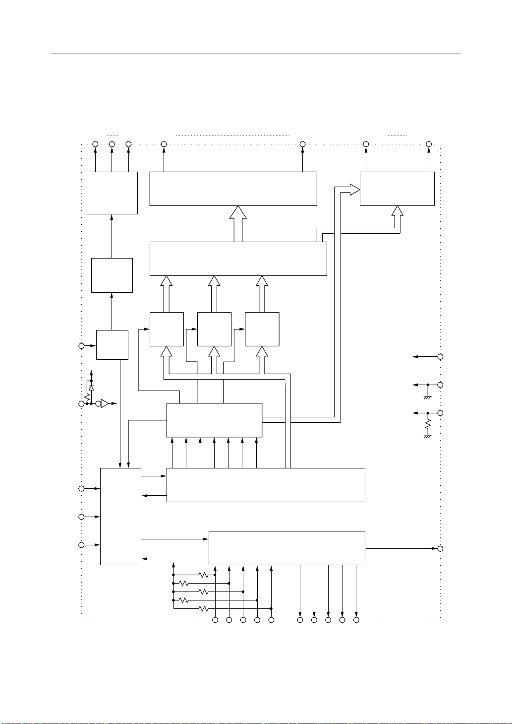
BLOCK DIAGRAM
MSM9006-01
MSM9006-01, -02¡ Semiconductor
SEG1 SEG35COM3COM1 SEG36/P05 SEG41/LED
OSC
RESET
COMMON
DRIVER
TIMING
GEN
OSC
35 OUT SEGMENT DRIVER
41 BIT DATA SELECTOR
41 BIT
LATCH
41 BIT
LATCH
MODE
SELECTOR
41 BIT
LATCH
5 SEGMENT/PORT
& SEGMENT/LED
DRIVER
V
DD
V
SS
TEST
LOAD
DATAI/O
CLOCK
CONTROL
LOGIC
C6 C5 C4 C3 C2 C1 C0
(41+7) 48 BIT SHIFT REGISTER
5¥5 KEY SCANNER
C0 C1 C2 C3 C4 R0 R1 R2 R3 R4
INT
2/18
Page 3
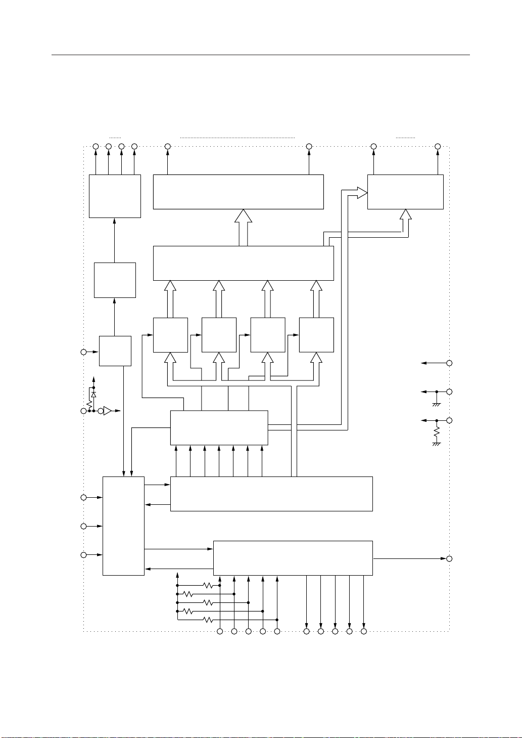
BLOCK DIAGRAM
MSM9006-02
MSM9006-01, -02¡ Semiconductor
SEG1 SEG35COM4COM1 SEG36/P05 SEG41/LED
OSC
RESET
COMMON
DRIVER
TIMING
GEN
OSC
35 OUT SEGMENT DRIVER
41 BIT DATA SELECTOR
41 BIT
LATCH
41 BIT
LATCH
MODE
SELECTOR
41 BIT
LATCH
41 BIT
LATCH
5 SEGMENT/PORT
& SEGMENT/LED
DRIVER
V
DD
V
SS
TEST
LOAD
DATAI/O
CLOCK
CONTROL
LOGIC
C6 C5 C4 C3 C2 C1 C0
(41+7) 48 BIT SHIFT REGISTER
5¥5 KEY SCANNER
C0 C1 C2 C3 C4 R0 R1 R2 R3 R4
INT
3/18
Page 4
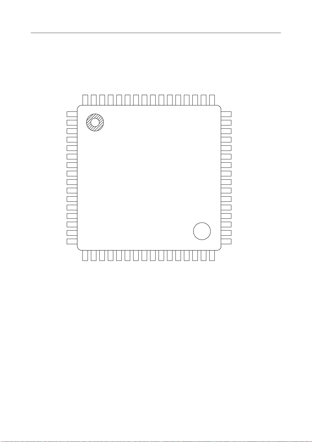
PIN CONFIGURATION (TOP VIEW)
MSM9006-01
COM1
COM2
COM3NCC0C1C2C3C4R0R1
6463626160595857565554
53 R2
52 R3
54 R4
50 LOAD
MSM9006-01, -02¡ Semiconductor
49 CLOCK
SEG1
SEG2
SEG3
SEG4
SEG5
SEG6
SEG7
SEG8
SEG9
SEG10
SEG11
1
2
3
4
5
6
7
8
9
10
11
12SEG12
13SEG13
14SEG14
15SEG15
16SEG16
1718192021222324252627
SEG17
SEG18
SEG19
SEG20
SEG21
SEG22
SEG23
SEG24
SEG25
SEG26
28SEG28
SEG27
29SEG29
30SEG30
31SEG31
32SEG32
48
DATA I/O
47
INT
46
RESET
45
TEST
44
V
SS
OSC
43
V
42
DD
SEG41/LED
41
SEG40/PO1
40
SEG39/PO2
39
SEG38/PO3
38
37 SEG37/PO4
36 SEG36/PO5
35 SEG35
34 SEG34
33 SEG33
NC: No-connection pin
64-Pin Plastic QFP
4/18
Page 5
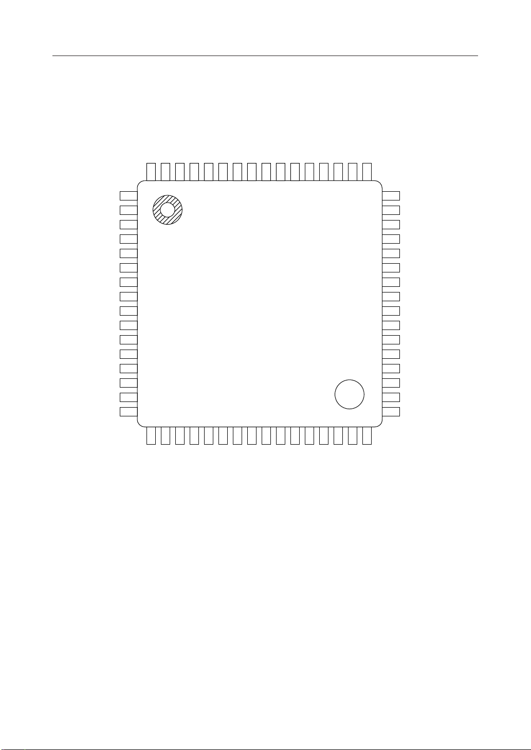
PIN CONFIGURATION (TOP VIEW)
MSM9006-02
COM1
COM2
COM3
COM4C0C1C2C3C4R0
6463626160595857565554
R1
53 R2
52 R3
54 R4
50 LOAD
MSM9006-01, -02¡ Semiconductor
49 CLOCK
SEG1
SEG2
SEG3
SEG4
SEG5
SEG6
SEG7
SEG8
SEG9
SEG10
SEG11
1
2
3
4
5
6
7
8
9
10
11
12SEG12
13SEG13
14SEG14
15SEG15
16SEG16
1718192021222324252627
SEG17
SEG18
SEG19
SEG20
SEG21
SEG22
SEG23
SEG24
SEG25
SEG26
28SEG28
SEG27
29SEG29
30SEG30
31SEG31
32SEG32
48
DATA I/O
47
INT
46
RESET
45
TEST
44
V
SS
OSC
43
V
42
DD
SEG41/LED
41
SEG40/PO1
40
SEG39/PO2
39
SEG38/PO3
38
37 SEG37/PO4
36 SEG36/PO5
35 SEG35
34 SEG34
33 SEG33
64-Pin Plastic QFP
5/18
Page 6
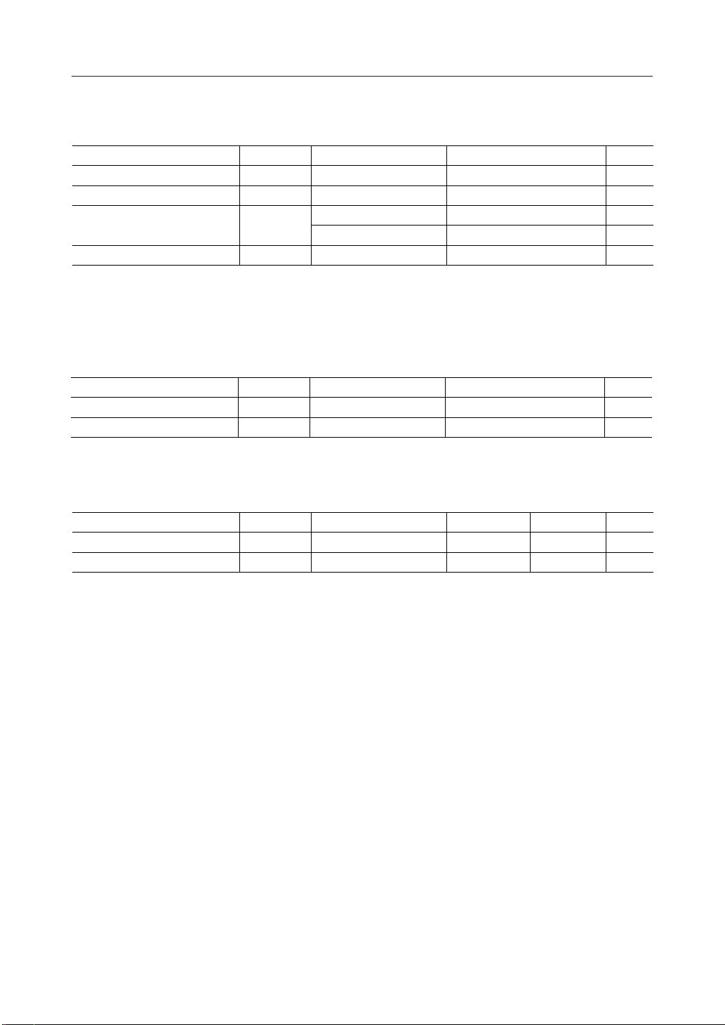
ABSOLUTE MAXIMUM RATINGS
Paramater Symbol Condition Rating Unit
Supply Voltage V
Input Voltage V
Output Current
Storage Temperature T
DD
I
STG
I
O
Ta=25°C –0.3 to +6.5 V
Ta=25°C –0.3 to VDD+0.3 V
Ta=25°C –20 mA
Ta=25°C –3 mA
— –55 to +150 °C
*1 Applies to LED output.
*2 Applies to port output.
RECOMMENDED OPERATING CONDITIONS
Paramater Symbol Condition Range Unit
Supply Voltage V
Operating Temperature T
DD
op
VSS=0V 4.5 to 5.5 V
— –40 to +85 °C
MSM9006-01, -02¡ Semiconductor
*1
*2
Recommended Oscillation Circuit Conditions
Paramater Symbol Condition Min. Unit
Oscillation Resistance R
Oscillation Capacitance C
O
O
Max.
—20 kW
— 0.01 mF
82
0.047
6/18
Page 7

ELECTRICAL CHARACTERISTICS
DC Characteristics
Parameter Symbol Condition Unit
"H" Input Voltage
"L" Input Voltage
"H" Input Voltage
"L" Input Voltage
"H" Input Current
"L" Input Current
"H" Input Current
"L" Input Current
"L" Input Current
"L" Input Current I
Segment Output
Voltage
Common Output
Voltage
"H" Output Voltage
"L" Output Voltage
"H" Output Voltage
"L" Output Voltage
"H" Output Voltage
"L" Output Voltage
"H" Output Voltage
"L" Output Voltage
Current Consumption
V
IH1
V
IL1
V
IH2
V
IL2
I
IH1
I
IL1
I
IH2
I
IL2
I
IL3
IL4
V
OS0
V
OS1
V
OS2
V
OS3
V
OC0
V
OC1
V
OC2
V
OC3
V
OH1
V
OL1
V
OH2
V
OL2
V
OH3
V
OL3
V
OH4
V
OL4
I
DD
=5.5V
V
DD
V
=5.0V
DD
VDD=4.5V
VDD=5.5V
—
—
—
—
V
I=VDD
VI=0V
V
I=VDD
VI=0V
=0V
V
I
VI=0V mA–0.1–0.02
=–10mA
I
O
=±10mA
I
O
=±10mA
I
O
=10mA
I
O
=–10mA
I
O
=±10mA
I
O
=±10mA
I
O
=10mA
I
O
=–15mA
I
O
=0.1mA
I
O
=–2mA
I
O
=1mA
I
O
=–0.4mA
I
O
=0.4mA
I
O
=–50mA
I
O
=1.0mA
I
O
No load
MSM9006-01, -02¡ Semiconductor
(VDD=5V±10%, Ta=–40 to +85°C)
Max.Min.
0.8V
DD
V
SS
0.7V
DD
V
SS
–0.7
DD
–0.65
DD
2/3VDD–0.65
1/3VDD–0.65
—
2/3VDD+0.72/3VDD–0.7
1/3VDD+0.71/3VDD–0.7
2/3VDD+0.65
1/3VDD+0.65
VSS+0.65
DD
DD
DD
DD
VV
V0.2V
VV
V0.3V
mA1—
mA–1—
mA10—
mA–10—
mA–0.9–0.18
V—V
V
V
VVSS+0.7—
V—V
V
V
V
V—3.0
V0.4—
V—3.5
V1.0—
V—4.1
V0.4—
V—2.5
V0.4—
mA0.45—
Applicable Pin
*1
C0 to C4
CLOCK, LOAD
DATA I/O
C0 to C4
RESET
SEG1 to SEG35,
SEG36/PO5 to
SEG41/LED
*2
COM1 to COM4
SEG41/LED
*3
SEG36/PO5 to
SEG40/PO1 *4
DATA I/O
INT
R0 to R4
*5
V
DD
*1 CLOCK, LOAD, DATA I/O and RESET
*2 When SEG36/PO5-SEG41/LED are used as LCD segment output pins.
*3 When SEG41/LED is used as output pin for LED driving.
*4 When SEG36/PO5-SEG40/PO1 are used as general purpose port output pins.
*5 When key data that corresponds to C0-C4 is on one of the lines to which the R0-R4 pins are
connected, the key data is not identified if the line is at a "H" level.
Therefore, as long as the value of V
is 2.5V or greater, key data is identified correctly.
OH4
7/18
Page 8

MSM9006-01, -02¡ Semiconductor
Switching Characteristics
=5V±10%, Ta=–40 to +85°C)
(V
DD
Paramater Symbol Condition Min. Unit
Clock Frequency f
Clock Pulse Width t
CP
WCP
Rise/Fall Time tr, t
Data Setup Time t
Data Hold Time t
Load Pulse Width t
ClockÆLoad Time t
LoadÆClock Time t
Output Delay Time 1 t
Output Delay Time 2 t
DSU
DHD
WLD
CL
LC
pd1
pd2
— — MHz
— 200 ns
f
—— ns50
— 100 ns—
— 100 ns—
— 200 ns—
— 100 ns—
— 200 ns—
CL=50pF — ns300
*1
—— ns300
Max.
2.0
—
*1 Since the DATA I/O pin input-output state is undefined for 300ns after the rising edge of
LOAD when changing from output mode to input mode, do not input any signal to the
DATA I/O pin for this period.
t
r
0.8V
CLOCK
t
t
DHD
DSU
DATAI/O
0.8V
DD
0.2V
DD
(During input mode)
LOAD
LOAD
DATAI/O (
DATAI/O (
When changing from input mode to output mode)
When changing from output mode to intput mode)
t
WCP
t
WCP
t
f
DD
0.2V
DD
1/f
CP
t
WLD
0.8V
t
CL
HiZ
0.8V
DD
0.2V
DD
DD
t
LC
0.2V
DD
t
pd1
0.8V
DD
0.2V
DD
t
pd2
t
pd1
HiZ
The duration of charge or discharge at
the high-impedance period is determined
by the wiring resistance and the wiring
capacitance.
8/18
Page 9

MSM9006-01, -02¡ Semiconductor
FUNCTIONAL DESCRIPTION
Pin Functional Description
• OSC
This is an input pin for the oscillator to generate LCD AC lighting and keyscan signals. Connect
external capacitor and resistor as shown below to form RC oscillation circuit.
The relationship between frame frequency f
f
is:
OSC
f
FRM
= f
OSC
/24, T
SCN
= 20/f
OSC
, keyscan period T
FRM
, and oscillation frequency
SCN
(See REFERENCE DATA for information on the relationship between CO, RO values, frame
frequency, and keyscan periods.)
V
DD
R
O
OSC
C
O
• DATA I/O
This is a serial data input/output. The pin is in output state for the duration from the first shift
clock rising after "Key Data Output" command is entered, to the load signal rising, and in input
state otherwise. (The pin is in input state after reset.)
The relationship between data level and operation is shown below.
Data Level
"H"
"L"
LCD and LED Display
ON
OFF
Port
"H"
"L"
Key Status
ON
OFF
• CLOCK
This is an input pin for the shift clock. DATA I/O pin data is either input or output in
synchronization with the rising of the clock.
• LOAD
This is a load signal input pin. It is used for transferring serial input data to a latch for display,
entering commands, or resetting the output state of the DATA I/O pin.
9/18
Page 10

MSM9006-01, -02¡ Semiconductor
• R0 - R4
These are keyswitch scan signal output pins. During the scan operation, "L" level is output in
the order of R0, R1, …, R4. All signals go to "L" level when scanning stops. (See keyscan)
• C0 - C4
These are input pins that detect the key status. Pull-up resistor is included. Key matrices are
formed with R0 -␣ R4 pins.
C0 C1 C2 C3 C4 R0 R1 R2 R3 R4
• INT
This is the keyscan end signal output pin. This pin goes to "H" level when one scan cycle ends,
and returns to "L" level by a load signal after data is output or after the "Keyscan Stop" command
is entered. (This pin also returns to "L" level at reset.)
10/18
Page 11

MSM9006-01, -02¡ Semiconductor
• RESET
This is the reset signal input pin that initializes the device, and it is activated at "L" level. Pullup resistor is included. The power-on reset operation is performed by externally connecting a
capacitor. (See "Power-on Reset" in REFERENCE DATA)
V
DD
RESET
• SEG1 - SEG35
These are output pins for the LCD display, and are connected to the segment pins of the LCD
panel. See the section on data configuration for the correspondence between SEG output and
input data.
• COM1 - COM4
These are output pins for the LCD display, and are connected to the common pins of the LCD
panel.
In the case of MSM9006-01, the COM1 to COM3 pins apply.
• SEG36/PO5 - SEG40/PO1
These pins can select the output pins for the LCD display (segment pins) or general port output
pins by setting with commands.
• SEG 41/LED
This is an output pin for the LCD display (segment), or LED drive selection with command. If
LED drive is selected, the LED and current limit resistor are externally connected.
SEG41/LED
• TEST
This is an input pin for IC testing. This pin should be connected to V
• VDD, V
SS
SS.
These are power supply and ground pins.
11/18
Page 12

MSM9006-01, -02¡ Semiconductor
,,,
,,,,,,,,,,,,,,,,
p
Display Data Input
As shown in the section on data configuration, the data for display consists of data field
corresponding to segments ON/OFF and of command field indicating display data input.
Set the C0 and C1 bits of the command field according to the COM pins corresponding to the
display data. LED display data when LED display pin is selected and output port data when
output port pin is selected correspond to common 1. Data input to the DATA I/O pin is
caputured by a shift register at the rising edge of a clock signal, then it is transferred to a data
latch for display when the LOAD signal is at "H" level, and is then output through a segment
driver.
CLOCK
DATA I/O
LOAD
Display Output
D1 D2 D3 D4 C1 C2 C3C0D41D40
C4 C5 C6
Old Data New Data
Key Data Output
The status of a key switch is indicated by ON = 1, OFF = 0, and is read as 25-bit serial data. (For
information on the sequence, see the section on data configuration.) To output data, the "Key
Data Output" command is first entered. Then data is output synchronizing with the rising edge
of a clock signal. If a LOAD pulse is then added, the DATA I/O pin returns to the input status,
and the next data or command can be input.
CLOCK
DATA I/O
C3
C4 C5 C6 01 02 03 024 025
LOAD
Next Command
ut
In
12/18
Output Command Write
Key Data Read
Page 13

MSM9006-01, -02¡ Semiconductor
Keyscan
Keyscan starts when the key status is changed, or when the "Keyscan Start + key data output"
command is entered. Scan continues until the "Keyscan Stop" command is entered. (Scan is in
stop state at power-on reset.)
When 1 keyscan cycle ends, the INT signal goes to "H" level, so this signal can be used as an
interrupt flag. The INT signal is reset when the LOAD pulse is input after the key data is output,
when the "Keyscan Stop" command is entered, or when a reset signal is applied.
T
SCN
R0
R1
R2
R3
R4
INT
Keyscan Start Command Entered,
or Key Status Changed
Data Read Data Read
Data Read
Keyscan Stop
Command Entered
Notes: 1. A recognition error (that is, a switch that was not pressed is recognized as being
pressed) may occur when three or more key switches are pressed at the same time.
If simultaneous pressing of three or more key switches must be recognized, insert
diodes serially to each switch. If simultaneous pressing of three or more key switches
is required not to be recognized, a possible approach is to program so that the entire
key information will be ignored if there are three or more 1s in read data.
2. A change of key status is detected as a change of column inputs (C0 - C4). Therefore
if multiple switches which connected to the same column are pressed at the same
time, it will not be detected as a change of key status.
13/18
Page 14

MSM9006-01, -02¡ Semiconductor
Display ON, Display OFF
Upon power-on reset, the display is put in off state. To turn on the display, enter the Display
ON command.
Regardless of the display data, the display goes out by entering the Display OFF command
because the Display OFF command turns off all segments and LED display and changes the
state of the output port from "H" to "L" level.
The display returns to the initial state by entering the Display ON command because the Display
ON command resets the off-state of the display.
CLOCK
DATA I/O
LOAD
Display ON/OFF
RESET
D1 D2 C5 C6 C2 C3 C4 C5 C6 C2 C3 C4 C5 C6
Display Data Input Period
+F9 Command
Display On Command
Entry Timing
Display Off Command
Entry Timing
14/18
Page 15

Command List
MSM9006-01, -02¡ Semiconductor
Command
F1
F2
F3
F4
F5
F6
F7 0 Keyscan Stop100¥¥¥
F8 0 Keyscan Start + Key Data Output111¥¥¥
F9 1 LCD/Output Port, LED Pin SettingS/P5 S/P4 S/P3 S/P2 S/P1 S/L
C6
C5
C4
C3
C2
C1
C0
Display Data Input (Corresponds to common 1)
0
0
1
0
0
0
1
0
1
0
0
1
0
¥
¥
0
0
0
1
1
0
1
0
1
0
1
0
¥
0
1
0
1
1
¥
0
1
1
0
¥
¥
Display Data Input (Corresponds to common 2)
Display Data Input (Corresponds to common 3)
0
Display Data Input (Corresponds to common 4)
1
Key Data Output
¥
Display Data Input (1) + Key Data Output
0
Display Data Input (2) + Key Data Output
1
Display Data Input (3) + Key Data Output
0
Display Data Input (4) + Key Data Output
1
Display OFF
¥
Display ON
¥
Keyscan Stop + Key Data Output
¥
Operation
(*2)
(*2)
(*1)
¥ : Don't care
*1 The bits C5-C0 correspond to SEG36/PO5, SEG37/PO4, SEG38/PO3, SEG39/PO2, SEG40/
PO1, and SEG41/LED pin, respectively.
The high level selects the LCD (SEG36-SEG41) output. The low level selects the output port
(PO5-PO1) and LED output (any pin combination is selectable).
Because the pin select mode is not set upon power-on reset, be sure to put the device into pin
select mode before entering the Display On command.
*2 Out of the eight F1 and F3 commands, only those that correspond to common 1-3 are valid
in the case of the MSM9006-01. (Common 4 is not available in the MSM9006-01.)
15/18
Page 16

Data Configuration
Input data
Last Bit
MSM9006-01, -02¡ Semiconductor
First Bit
(Corresponds to SEG 41/LED)
Corresponds to
SEG 40/PO1
Corresponds to
SEG 35/PO5
Corresponds
to SEG 35
Corresponds
to SEG 1
C6 C5
C1 C0 D41 D40
C2
C3 D1D2D6
C4
Command
LCD Display Data
D8
D7
LCD/LED Display Data
LCD Display/Port Data
Notes: 1. LED data when the LED pin is selected and output port data when an output port
pin is selected, correspond to common 1 side (C0, C1=0).
2. The commands F2, F6-F8 are enabled when only the 4 bits of C3-C6 are input. The
commands F4 and F5 are enabled when only the 5 bits of C2-C6 are input. (Bits D1D41, C0-C1 are not required.)
3. If dummy bits are required depending on the number of transfer bits, insert them
into the first bit side.
Output data
Last Bit First Bit
01025
R4 R3 R2 R1 R0
C4 C3 C2 C1 C0 C4 C3 C2 C1 C0 C4 C3 C2 C1 C0 C4 C3 C2 C1 C0 C4 C3 C2 C1 C0
16/18
Page 17

REFERENCE DATA
500
400
300
MSM9006-01, -02¡ Semiconductor
= 5V
V
DD
Ta = 25°C
2
3
[Hz]
FRM
f
200
150
100
70
50
30
20
20 33 39 62 82
RO [kW]
CO=0.01mF
C
=0.022mF
O
=0.033mF
C
O
C
=0.047mF
O
4
5
6
8
10
15
20
30
40
50
[ms]
SCN
T
f
FRM
and T
vs. RO vs. C
SCN
O
• Power-on Reset
The capacitance of an external capacitor connected to the RESET pin should be:
C
(ex. C
≥ 12.5 ¥ T
RST
≥ 0.125 (mF) if T
RST
(mF)
R
=10 (ms))
R
When TR is the rise time for power supply connected to the MSM9006 and C
capacitance of a capacitor connected to the RESET pin.
The pulse width of an external reset signal should be more than TR.
RST
is the
17/18
Page 18

PACKAGE DIMENSIONS
QFP64-P-1414-0.80-BK
Mirror finish
MSM9006-01, -02¡ Semiconductor
(Unit : mm)
Package material
Lead frame material
Pin treatment
Solder plate thickness
Package weight (g)
Epoxy resin
42 alloy
Solder plating
5 mm or more
0.87 TYP.
Notes for Mounting the Surface Mount Type Package
The SOP, QFP, TSOP, SOJ, QFJ (PLCC), SHP and BGA are surface mount type packages, which
are very susceptible to heat in reflow mounting and humidity absorbed in storage.
Therefore, before you perform reflow mounting, contact Oki’s responsible sales person for the
product name, package name, pin number, package code and desired mounting conditions
(reflow method, temperature and times).
18/18
 Loading...