

Page 1

E2B0041-27-Y3
¡ Semiconductor
¡ Semiconductor
This version: Nov. 1997
Previous version: Mar. 1996
MSM9000B-xx
MSM9000B-xx
DOT MATRIX LCD CONTROLLER
GENERAL DESCRIPTION
The MSM9000B-xx is a dot-matrix LCD control driver which has functions of displaying 12 (5
x 7 dots) characters (2 lines) and 120-dot arbitrators.
The MSM9000B-xx is provided with a 16-dot common driver, 60-dot segment driver, Display
Data RAM (DDRAM), and Character Generator ROM (CGROM).
This device can be controlled with commands entered through the serial interface or parallel
interface.
The font data in the CGROM can be changed by mask option.
Since the MSM9000B-xx has an LCD driving bias generator circuit, LCD bias voltages can be
obtained by merely providing a required capacitance externally.
The MSM9000B-xx is applicable to a variety of LCD panels by controlling the contrast.
FEATURES
• Logic voltage(VDD): 2.5 to 3.3 V
• LCD driving voltage(VBI) : 3.0 to 5.5 V
• Low current consumption: 35 mA max.(operating)
• Switchable between 8-bit serial interface and 8-bit parallel interface
• Contains a 16-dot common driver and a 60-dot segment driver
• Contains CGROM with character fonts of (5 x 7 dots) x 256
• Built-in bias voltage generator circuit
• Built-in contrast adjusting circuit
• Built-in 32.768 kHz crystal oscillator circuit
• Provided with 120 dot arbitrators
• 1/9 duty mode (1 line : characters, 2 lines : arbitrators)
1/16 duty mode (2 lines : characters, 2 lines : arbitrators)
• Character blink operation can be switched between all-character lighting-on mode and allcharacter lighting-off mode.
• Package:
TCP mounting with 35 mm wide film ; Tin-plated (Product name : MSM9000B-xx AV-Z-xx)
Chip (Product name : MSM9000B-xx)
xx indicates code number.
1/38
Page 2
¡ Semiconductor
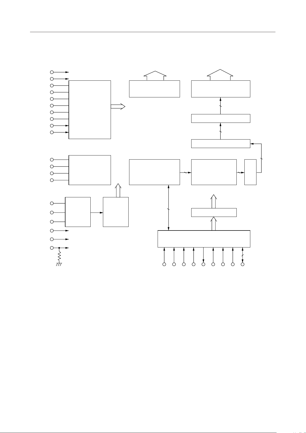
BLOCK DIAGRAM
MSM9000B-xx
V
DD
V
SS
V
SS1
V
SS2, 3
V
SS4
V
SS5
V
C2
V
CC2
N1
N2
V
SS6
V
SH
V
C1
V
CC1
XT
XT
32K/EXT
Regulator
+
Halver & Voltage
Multiplier(4-fold)
Voltage Multiplier
(3/2-fold)
Crystal OSC
Circuit
Timing
Circuit
C1-C16
Common
Driver
LCD bias
Display Data RAM
(DDRAM) (456 Bits)
S1-S60
6016
Segment Driver
60
Latch
60
Shift Register
5
Character Generator
8
ROM (CGROM)
F/F
5
Gate
(256 ¥ 5 ¥ 7 Dots)
8
Registers
9D/16D
RESET
TEST
I/O Interface
8
P/S CS C/D SHT SO SI WR RD DB7-0
2/38
Page 3
¡ Semiconductor
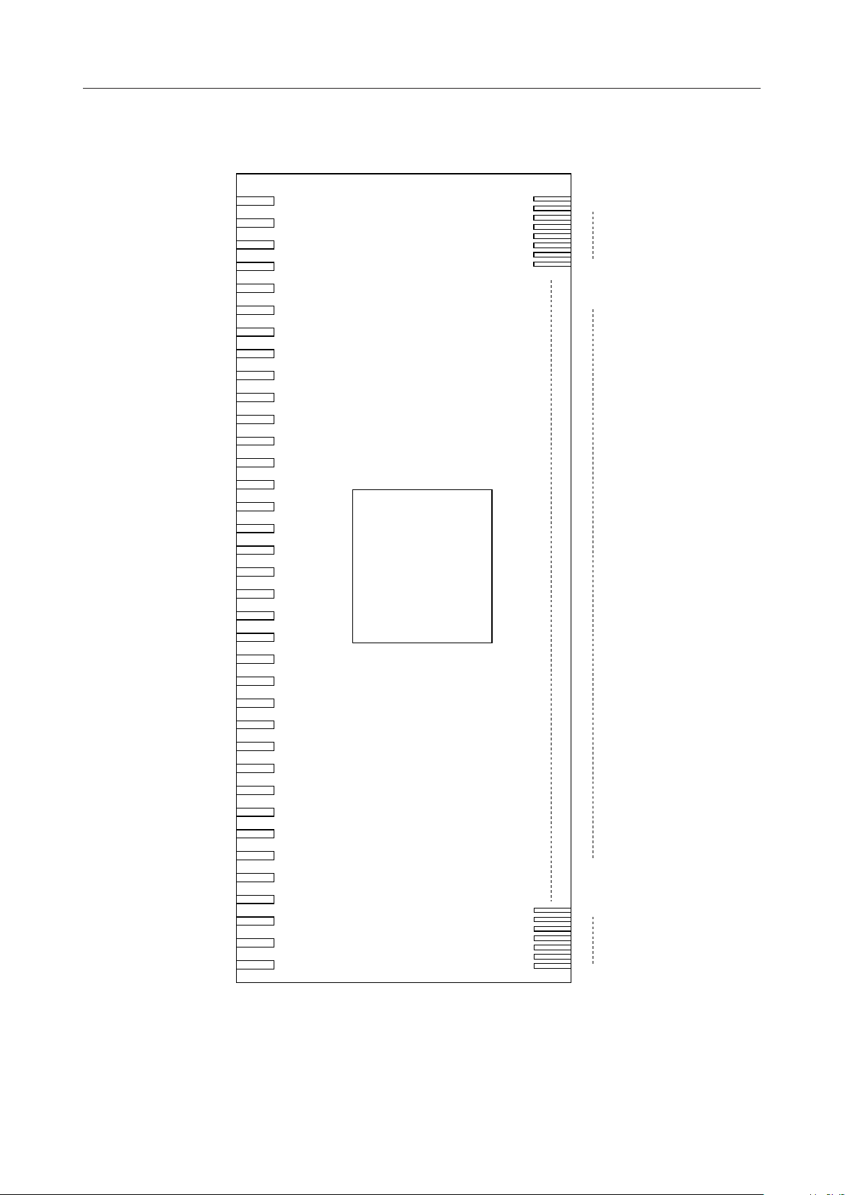
PIN CONFIGURATION
MSM9000B-xx
RESET
32K/EXT
9D/16D
P/S
XT
XT
V
SS
CS
C/D
RD
WR
SI
SHT
SO
DB7
DB6
DB5
DB4
DB3
DB2
DB1
DB0
V
DD
TEST
N1
N2
V
CC1
V
C1
V
SH
V
SS6
V
CC2
V
C2
V
SS1
V
SS2, 3
V
SS4
V
SS5
COM1
COM8
SEG1
SEG2
SEG59
SEG60
COM16
COM9
Pin Configuration Viewed From Pattern
3/38
Page 4
¡ Semiconductor
PIN DESCRIPTIONS
MSM9000B-xx
Function Type Description
Symbol
Number
of Pins
CPU Interface I Chip select input signal
Oscillation I Crystal oscillation input, clock input
Control Signal I Parallel/Serial interface switching signal input
CS
WR
RD
C/D
DB0-7
SI
SO
SHT
XT
XT
P/S
9D/16D
32K/EXT
RESET
1
1
1
1
8
1
1
1
I Write enable signal, latch for serial interface
I Read enable signal
Command/Data select input signalI
I/O 8-bit parallel data inputs/outputs
I Serial data input
O Serial data output
I Shift clock input for data input in serial interface mode
1
1
O Crystal oscillation output
1
1
1
1
I Duty select signal input
I Clock select signal input
I Reset is performed by setting the RESET input to "L"
level
N1, N2
TEST
LCD Driving
Output
Power Supply — Positive + power supply pin for LOGIC
SEG1-SEG60
COM1-COM16
V
DD
V
SS
V
, V
SS1
SS2, 3
V
, V
SS4
SS5
V
SS6
V
SH
VC1, V
CC1
VC2, V
CC2
60
16
2
1
I Contrast control signal input
I Test signal input. Fix to "L" Level or leave open
O Segment outputs for LCD driving
O Common outputs for LCD driving
1
1
4
1
1
2
2
— GND pin
— Boosted voltage output pins & bias power supply pins
— Voltage multiplier output pin (3-/2-fold)
— Haver output pin
— Voltage multiplier (3-/2-fold)
— Voltage multiplier (4-fold)
112Total
4/38
Page 5
¡ Semiconductor
ABSOLUTE MAXIMUM RATINGS
MSM9000B-xx
Parameter Symbol Condition Rating Unit
Power supply voltage V
Bias voltage V
Input voltage V
DD
Ta=25°C, V
BI
I
Ta=25°C, VDD–V
DD–VSS
SS5
Ta=25°C V
–0.3 to +4.6
–0.3 to +7 V
–0.3 to VDD + 0.3
Applicable pin
V
V
, V
DD
SS
, V
V
DD
SS5
All input pins
Chip –55 to +150
Storage temperature
T
STG
TCP –30 to +85
°C
—
Ta: Ambient temperature
RECOMMENDED OPERATING CONDITIONS
Parameter Symbol Condition Range Unit
Power supply voltage V
Bias voltage V
IC source oscillation f
Operating temperature — –30 to +85T
DD
BI
int
op
*1 VDD is the highest pin and V
V
DD–VSS
*1, VDD–V
SS5
*2 kHz
the lowest for the bias voltage.
SS5
2.5 to 3.3
3 to 5.5 V
26 to 47
°C
*2 Connect the specified capacitors to the voltage doubler and LCD bias generator.
*3 Make sure that the crystal oscillation frequency or the divided clock frequency falls within
this range.
Applicable pin
V
, V
V
DD
V
DD, VSS5
*3
—
SS
Note 1: Ensure the chip is not exposed to any light.
Note 2: The bias voltage may exceed 5.5 V at some contrast stages. Adjust the stage with
software so that the bias voltage does not exceed 5.5 V.
5/38
Page 6
¡ Semiconductor
MSM9000B-xx
ELECTRICAL CHARACTERISTICS
DC Characteristics (1)
(V
= 2.5 to 3.3 V, VBI = 3 to 5.5 V, Ta = –30 to +85°C)
DD
Parameter Symbol Condition Min. Typ. Max. Unit
Input high voltage 1 V
Input high voltage 2 V
Input low voltage 1 V
Input low voltage 2 V
Input high current 1
Input high current 2
Input low current 1
Off leakage current
Output high voltage 1
Output low voltage 1 V SO and DB0 to
COM output resistance
I
I
I
V
IH1
IH2
IL1
IL2
IH1
IH2
IL1
off
OH
OL1
C
S
—V
— 0.8V
–0.25 — V
DD
DD
—VDDV Other inputs
DD
— 0 — 0.55 V
— 0 — 0.2V
VI=V
VI=V
DD
DD
—— 1
10 — 60
VI=0 V –1 — —
/0 V –1 — 1
V
I=VDD
I
=–500 mA
O
IO=500 mAV
=±50 mAR
I
O
I
=±20 mAR
O
0.9V
DD
——
— — 0.1V
——10
——30SEG output resistance kW SEG1 to SEG60
DD
DD
During operation *1
Drain current 1
DD1
Crystal oscillation
—1535
f = 32.768 kHz
During operation *1
Drain current 2
I
DD2
External clock
—1535mA
f = 32 kHz
Applicable pin
XT
V
XT
V Other input pins
Input pins other
mA
than XT and TEST
TEST (pull-down
mA
resistor)
mA
Input pins other
than XT and TEST
SO and DB0 to
mAI
DB7
V
SO and DB0 to
DB7
DB7
kW COM1 to COM16
mAI
V
DD
V
DD
I
DD3
During standby
—— 7Drain current 3 mAV
*1 No output load
Note : The values in this table are assured when the chip is not exposed to light.
DD
6/38
Page 7
¡ Semiconductor
MSM9000B-xx
DC Characteristics (2)
=0 V, VSS=–3 V, Ta=–30 to +85°C)
(V
DD
Parameter Symbol Condition Min. Typ. Max. Unit
Bias voltage 1 –V
SS1
–V
= "A"V 1/2A–0.1 1/2A 1/2A+0.1 V
SS2, 3
Applicable pin
V
N1 = "L", N2 = "L"
Bias voltages 2 and 3 –V
Bias voltage 4 –V
Bias voltage 5
Contrast pitch
–V
–V
SS2, 3
SS4
SS5
con
Contrast = "5"
–V
–V
= "A"V 3/2A–0.1 3/2A 3/2A+0.1 V V
SS2, 3
= "A"V 2A–0.2 2A 2A+0.2
SS2, 3
VBI for each stage 0.18 0.21 0.26
1.9 2.2 2.5 V V
V
V
V
Note 1: Connect a 0.1 µF capacitor to the LCD bias generator.
Note 2: The values in this table are assured when the chip is not exposed to light.
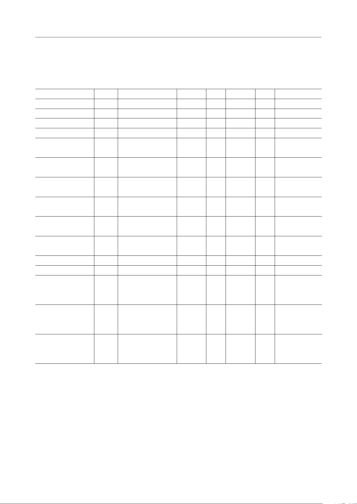
AC Characteristics
Parallel interface
(VDD=2.5 to 3.3 V, VBI=3 to 5.5 V, Ta=–30 to +85°C)
Parameter Symbol Condition Min.
RD high-level width t
WR high-level width t
WR low-level width —t
WR-RD high-level width —t
CS or C/D setup time —t
CS or C/D hold time —t
Write data setup time —t
Write data hold time —t
Read data output delay time CL=50 pFt
Read data hold time —t
External clock high-level width —t
External clock low-level width —t
RESET pulse width —t
Rise and fall time of external
clock
WRH
WRL
WWH
WWL
WWRH
AS
AH
DSW
DHW
DDR
DHR
WCH
WCL
WRE
, t
r
— 200
—RD low-level width t
200
— 200
200
200 — ns
50 — ns
0—ns
50 — ns
50 — ns
— 200 ns
20 — ns
1—ms
1—ms
2.0 — ms
f
—t
— 100 ns
Max.
—
—
—
—
SS1
SS2, 3
SS4
SS5
—
Unit
ns
ns
ns
ns
Note: The values in this table are assured when the chip is not exposed to light.
7/38
Page 8

¡ Semiconductor
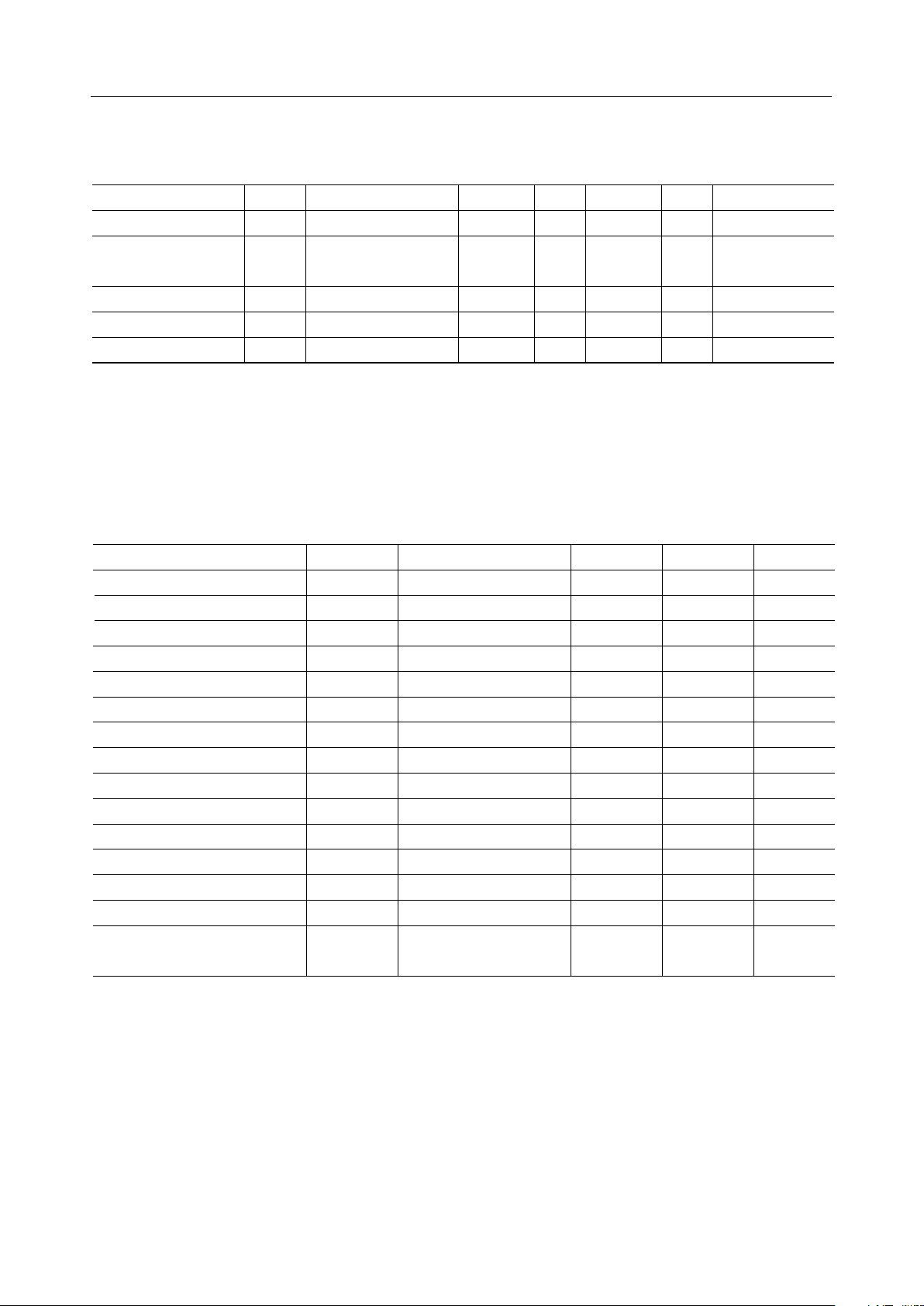
Serial interface
Parameter Symbol Condition Min.
CS or C/D setup time t
SI setup time t
SI hold time —t
SHT high-level pulse width —t
SHT low-level pulse width —t
SHT clock cycle time —t
SO ON delay time CL= 50 pFt
SO output delay time CL= 50 pFt
SO OFF delay time —t
BUSY delay time CL= 50 pFt
WR setup time —t
WR low-level pulse width —t
RESET pulse width —t
Rise and fall time of external
clock
SAS
SAH
IS
IH
WSHH
WSHL
SYS
ON
DS
OFF
BUSY
SHS
WWL
WRE
, t
r
MSM9000B-xx
(VDD = 2.5 to 3.3 V, VBI = 3 to 5.5 V, Ta = –30 to +85°C)
Max.
— 100
—CS or C/D hold time t
20
— 100
20
—
—
—
—
100 — ns
100 — ns
400 — ns
— 200 ns
0 200 ns
— 100 ns
— 200 ns
200 — ns
120 — ns
2.0 — ms
f
—t
— 100 ns
Unit
ns
ns
ns
ns
Note: The values in this table are assured when the chip is not exposed to light.
8/38
Page 9
¡ Semiconductor
Timing Diagram for the Parallel Interface
—
V
CS
C/D
WR
IH
—
V
IL
—
V
IH
—
V
IL
t
AS
—
V
IH
—
V
IL
t
WRH
t
WWL
MSM9000B-xx
t
AH
t
WWH
t
WWRH
t
AS
t
WRL
t
AH
RD
DB0-7
RESET
XT
—
V
IH
—
V
IL
t
DSW
V
IH
V
IL
t
WRE
—
V
IL
t
r
—
V
IH
—
V
IL
t
DHW
t
f
t
WCL
t
DDR
V
OH
V
OL
t
WCH
t
DHR
V
IH
V
OH
= 0.8VDD,
= 0.9VDD,
V
V
= 0.2V
IL
OL
= 0.1V
DD
DD
9/38
Page 10
¡ Semiconductor
Timing Diagram for the Serial Interface
—
V
CS
C/D
SI
SHT
IH
—
V
IL
—
V
IH
—
V
IL
—
V
IH
—
V
IL
t
SAS
—
V
IH
t
t
IS
IH
50%
—
V
IL
t
WSHL
t
WSHH
t
SHS
MSM9000B-xx
t
SAH
WR
SO
RESET
XT
—
V
IH
—
V
IL
t
ON
—
V
OH
V
OL
V
IL
"Z"
—
—
t
—
V
IH
—
V
IL
t
SYS
t
DS
t
WWLtBUSY
t
OFF
"Z"
t
WRE
t
r
f
V
= 0.8 VDD,
IH
V
= 0.2 V
IL
DD
V
OH
= 0.9 VDD,
V
OL
= 0.1 V
DD
10/38
Page 11

¡ Semiconductor
MSM9000B-xx
FUNCTIONAL DESCRIPTION
Pin Functional Description
• CS (Chip Select)
Chip select input pin. A logic low on the CS input selects the chip and a logic high on the CS
input does not select the chip. Command and display data inputs can be enabled only when
the chip is selected.
When the input is high, the SO pin and DB0 to DB7 pins are in the high impedance state,
causing SHT, WR and RD pins high level internally.
• WR (Write Enable)
When the parallel interface is used, this pin is the write signal input. Data is written into the
register at the rising edge of WR pulse. When the serial interface is used, this pin is the latch
signal input. This pin is normally high.
• RD (Read Enable)
When the parallel interface is used, this pin is the read signal input. While the pulse is low,
data can be read. The pin is normally high. When this pin is made low with C/D set low, the
display data pointed to by the address pointer is output from DB0 to DB7. When the pin is
made low with C/D set high, busy data is output from DB0 and low signals are output from
DB1 to DB7. After the rising edge of WR, busy data (H) is output. The data automatically
changes to non-busy (L) after the specified time elapses.
When the serial interface is used, fix this pin to "H" or "L".
•C/D (Command/Data Select)
This input pin selects whether the data to be input to the SI pin and the DB7 to DB0 pins is
handled as a command or display data, depending on the state of the pin at the rising edge
of WR. When the pin is H, the input data is handled as a command. When the pin is L, display
data is input.
• DB0 to DB7 (Data Buses 0 to 7)
Data input and output pins for the parallel interface. Normally data buses 0 to 7 are in high
impedance, when RD is driven low, display data and the busy signal are output.
When the serial interface is used, leave this pin open.
• SI (Serial Data Input)
Data input pin for the serial interface. Commands and display data are read at the rising edge
of SHT and written to registers at the rising edge of WR. The eight-bit data immediately before
the rising edge of WR is valid.
When the parallel interface is used, fix this pin to "H" or "L".
• SO (Serial Data Output)
Data output pin for the serial interface. The display data pointed to by the address pointer is
output at the rising edge of SHT. After the rising edge of WR, busy data (H) is output.
The data automatically changes to non-busy (L) after the specified time elapses.
When the parallel interface is used, this pin remains in the high impedance state.
• SHT (Shift Clock)
Clock input pin to input and output serial interface data. Data input is synchronous with the
rising edge of the clock, and the data output is synchronous with the falling edge of the clock.
This pin is normally high.
When the parallel interface is used, fix this pin to "H" or "L".
11/38
Page 12
¡ Semiconductor
MSM9000B-xx
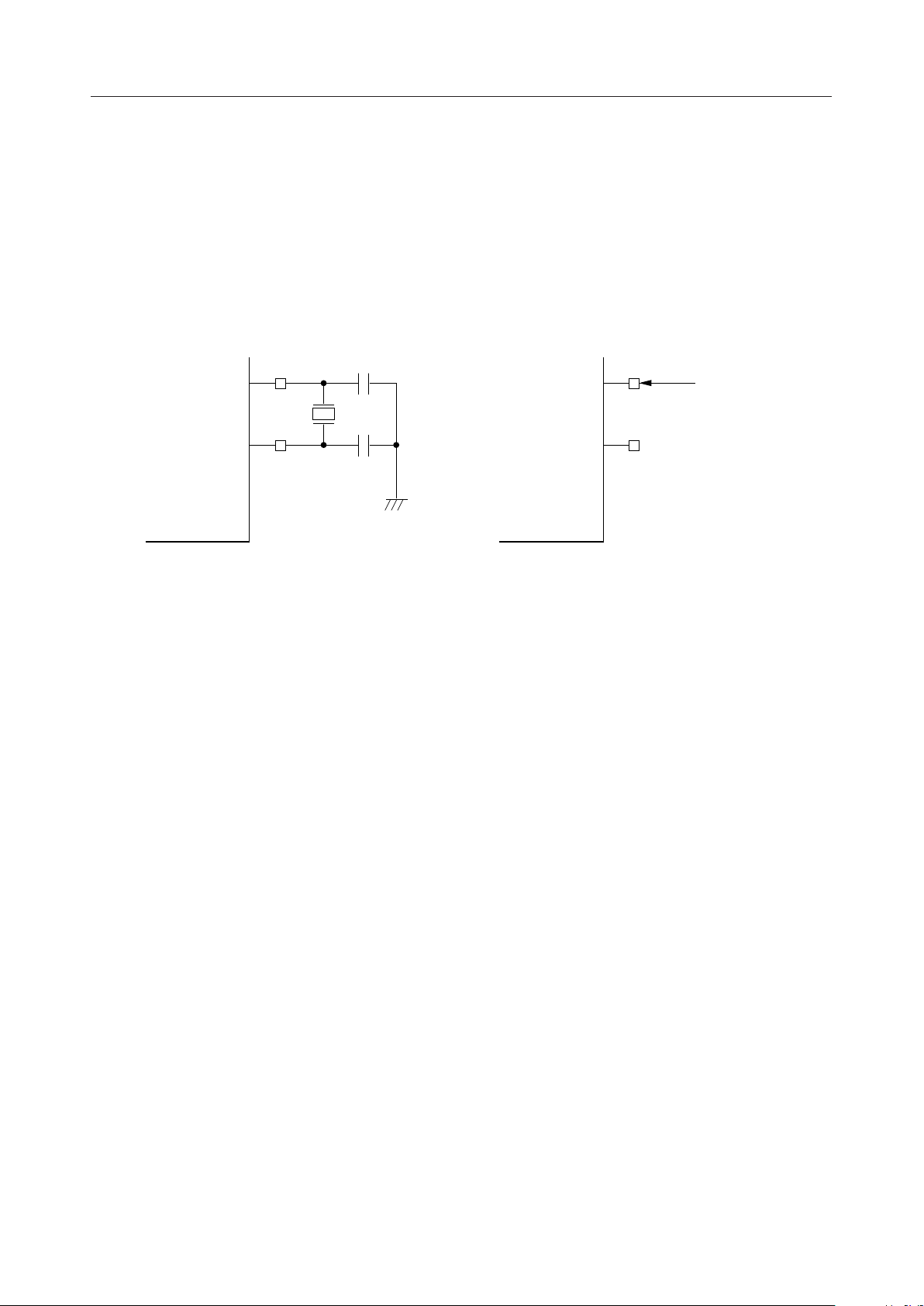
• XT (Crystal)
Input pin for crystal oscillation. By connecting a 32.768-kHz crystal and capacitors to this pin
and the XT pin, a crystal oscillation circuit is formed. When an external clock is used, input
the clock to the XT pin.
• XT (Crystal)
Output pin for crystal oscillation. By connecting a 32.768-kHz crystal and capacitors to this
pin and the XT pin, a crystal oscillation circuit is formed. When the external clock is used,
leave this pin open.
XT
18 pF
XT
18 pF
32.768 kHz
When forming a crystal oscillation circuit When inputting an external clock
XT
XT
External
clocks
OPEN
Oscillation circuit diagram
• P/S (Parallel/Serial Select)
Input pin to choose between the parallel interface and serial interface. To select the parallel
interface, make this pin low. To select the serial interface, make this pin high. After power
is turned on, do not change the setting of this pin.
• 9D/16D (Duty Select)
Input pin to set a duty cycle. When this pin is set to "H", a duty cycle of 1/9 is selected.
When the pin is set to "L", a duty cycle of 1/16 is selected. Choose either according to the panel
to be used. When a duty cycle of 1/9 is chosen, leave common output pins COM10 to COM16
open.
• 32K/EXT (Clock Select)
Input pin to choose crystal oscillation mode or external clock input mode. Leave this pin at
a "L" level.
• RESET (Reset)
Reset signal input pin. Setting this pin to L results in the initial state. For modes and the
display after a reset input, see "Mode Settings after a Reset Input".
• N1, N2 (Contrast Change)
Input pins that determine the voltages of V
SS2
and V
together with contrast adjustment by
SS3
a command. The table below shows the relationships between pin states and contrast
adjustment ranges.
12/38
Page 13

¡ Semiconductor
MSM9000B-xx
N1 N2
LL
LH
HL
HH
Contrast adjustment range by command
0 to 7
1 to 8
2 to 9
3 to A
• TEST (Test Signal)
Test signal input pin provided for test by the manufacturer. Fix this pin to L or leave it open.
• SEG1 to SEG60 (Segment 1 to Segment 60)
Segment signal output pins to drive the LCD. Leave the unused pins open.
• COM1 to COM16 (Common 1 to Common 16)
Common signal output pins to drive the LCD. When the duty cycle is 1/9, use COM1 to COM9
and leave COM10 to COM16 open.
•V
DD
Power supply pin to the logic section. Connect this pin to the positive terminal on the power
supply.
•V
SS
Pin to be connected to the GND power supply.
•V
SS1
, V
SS4
, V
SS5
Pins for voltage multiplier outputs and LCD power supply. Connect capacitors of 0.1 µF
between these pins and VDD for the charge distribution with V
capacitor and for voltage
SS2, 3
stabilization during generation of LCD bias voltages. The logical values of the LCD bias
voltage are as follows:
Highest voltage: V
Lowest voltage: V
DD
V
SS1=VSS2, 3
V
SS2, 3
V
SS4=VSS2, 3+VSS2, 3
SS5=VSS2, 3+VSS2, 3
/2
/2
/2+V
SS2, 3
/2
For both the 1/9 and 1/16 duty, 1/4 bias is used.
•V
SS2, 3
Voltage regulator output pin & LCD bias generator input used as a reference voltage for the
LCD bias generator.
Connect a capacitor of 0.1 µF between this pin and V
for charge distribution among
DD
capacitors and voltage stabilization during generation of various LCD bias voltages.
•V
SS6
Pin to connect the capacitor to store the 3-/2-fold voltage. Connect a capacitor of 0.1µF or more
between this pin and VDD.
•V
SH
Halves output pin for the voltage multiplier(3-/2-fold). Connect a 0.1 µF capacitor between
this pin and VDD.
13/38
Page 14

¡ Semiconductor
MSM9000B-xx
•VC1, V
CC1
Pins to connect the charge distribution capacitor used for the voltage malitiplier (3-/2-fold).
Connect a 0.1 µF capacitor between V
•VC2, V
CC2
and V
C1
CC1
.
Pins to connect the capacitor for charge distribution to generate LCD bias voltages on the basis
of V
. Connect a 0.1 µF capacitor between V
SS2, 3
and V
C2
CC2
.
14/38
Page 15

¡ Semiconductor
Parallel Interface Input-Output Timing
Input timing diagram
CS
C/D
MSM9000B-xx
DB7-0
WR
Output timing diagram
CS
C/D
RD
DATA
"H""L"
DB7-1
DB0
DATA "L"
DATA
When C/D="L", RAM display data is output on DB7-0 pins.
When C/D="H" and DB7-1="L", busy data is output on DB0 pin.
BUSY
15/38
Page 16

¡ Semiconductor
I/O Timings on the Serial Interface
Input timing diagram
CS
C/D
SHT
MSM9000B-xx
SI
WR
D7 D6 D5 D4
Output timing diagram
CS
C/D
SHT
D3
D2 D1 D0
SO
WR
BUSY BUSY
D7 D6 D5 D4
D3
D2 D1 D0
In SO output, the eight bits after the WR pulse is input are valid.
16/38
Page 17

¡ Semiconductor
MSM9000B-xx
LIST OF COMMANDS
*: Don't Care
No
Mnemonics
1 LPA Load Pointer
2 LOT Load Option 1011**I1I0Sets additional functions during execution of AINC.
3 SF Set Frequency1010**F1F0Sets conditions on master frequency.
4 BKCG 1/0 Bank Change 1/0 1 0 0*0001/0Valid only in 1/9 duty.
5 CONT U/D Contrast
Operation
76543210
1 1 A5 A4 A3 A2 A1 A0 Addresses 0-11, 16-27 for characters and
Address
100*0011/0Adjusts VLCD to 8 stages.
Up/Down
D
Comments
addresses 32-43, 48-59 for arbitrators
Changes display addresses 0-11, 16-27.
Adjustment range is changed by setting N1 and
N2 pins.
Contrast level is up if D0="1".
Contrast level is down if D0="0".
6 STOP Set
Stop Mode
7 SOE/D Serial Out
Enable/Disable
8 DISP Display On/Off 1 0 0 1/0 1 0 0 1/0 Display is ON if D0="1". Display is OFF if D0=0.
9 AINC Address
Increment
10 ABB Arbitrator Blink 1 0 0*1101/0Data that is input after setting D0="1", is set as data
11 CHB Character Blink 0 0 0*001/0*Controls blinking of character.
12 BPC Blink Pattern
Control
13 ABLC Arbitrator Line
Change
100*0100This mode is cancelled if D0="1" irrespective of
either "H" or "L" on C/D.
Stops oscillation and performs operation
equivalent to that of the DISP OFF command.
100*0111/0Switches between output and high impedance
of SO.
All commons and segments are at V
display is OFF.
Arbitrators alone are displayed if D4="1".
100*101*Pointer address is incremented by 1.
But, this command is invalid to operations that
are added by setting (I1, I0).
for arbitrator blink (1-dot unit).
This is cancelled by D0="0".
100*1111/0Sets blink patterns of characters.
( : chara) if D0="1", ( : chara) if D0="0".
011***L1L0Sets arbitrator display lines.
level if
DD
Notes :1 Pointer address is not changed even if commands numbers 1 to 8, 10, 12, 13 are enterd.
:2 Pointer address is automatically incremented by 1 when commands numbers 9, 11,
display code data, and arbitrator data are enterd.
17/38
Page 18

¡ Semiconductor
• LOT
I1 I0 RemarksAdditional function
00
01
10
11
No additional function
A blank code is written for each subsequent AINC.
Blinking is canceled for each subsequent AINC.
The above two functions are ORed.
•SF
F1 F0 RemarksFrequency of source oscillation in the IC
00
01
10
11
XT
XT ∏ 2
XT ∏ 4
XT ∏ 8
MSM9000B-xx
Used to automatically clear RAM at power-on.
Used to generate the optimum frequency when external
clocks are input.
•DISP
D4 D0 Character Arbitrator Remarks
*0
01
11
OFF OFF
ON ON
OFF ON
Used to turn on and off the display.
* : Don't care
• ABLC (when the duty is 1/16)
L1 L0 Arbitrator 1 Arbitrator 2 Remarks
00
01
1*
COM1 COM2
COM15 COM16
COM16 COM1
Arbitrator 1 indicates display data at addresses
32 to 43, while arbitrator 2 indicates display data
at addresses 48 to 59.
* : Don't care
• ABLC (when the duty is 1/9)
L1 L0 Arbitrator 1 Arbitrator 2 Remarks
00
01
1*
COM1 COM2
COM8 COM9
COM9 COM1
Arbitrator 1 indicates display data at addresses
32 to 43, while arbitrator 2 indicates display data
at addresses 48 to 59.
* : Don't care
18/38
Page 19

¡ Semiconductor
MSM9000B-xx
Explanation of Commands
[D7, D6, D5, D4, D3, D2, D1, D0], X = Don't care
• LPA (Load Pointer Address)
[1, 1, A5, A4, A3, A2, A1, A0]
This command sets in the address pointer the address of the command to be executed or the
address of the display data to be input. The settable addresses are inconsecutive addresses
00H to 0BH, 10H to 1BH, 20H to 2BH, 30H to 3BH represented by A5 to A0. When addresses
0CH to 0FH, 1CH to 1FH, 2CH to 2FH, or 3CH to 3FH are set, 00H is assumed.
After RESET = "L", the address is set to 00H.
• LOT (Load Option)
[1, 0, 1, 1, X, X, I1, I0]
This command executes the additional function specified by I1 and I0 to the display of the
current address when the AINC command is executed. Additional functions are shown
below.
After RESET = "L",, both I1 and I0 are set to "0".
I1 I0 Additional function
00
01
10
11
None
After this command is executed, the blank code is writtern each time AINC is executed.
After this command is executed, blinking is canceled each time AINC is executed.
The above two additional functions are ORed.
• SF (Set Frequency)
[1, 0, 1, 0, X, X, F1, F0]
This command sets the number by which the external clock input from the XT pin is divided
in order to get the source frequency inside the IC. This command is valid when 32K/EXT pin
is "L". The dividing ratio is specified by F1 and F0 in the command. The table below lists the
source oscillation frequencies in the IC.
After RESET = "L", both F1 and F0 are set to "0".
F1 F0 Frequency of source oscillation in the IC
00
01
10
11
XT
XT ∏ 2
XT ∏ 4
XT ∏ 8
• BKCG1/0 (Bank Change 1/0)
[1, 0, 0, X, 0, 0, 0, 1/0]
This command changes addresses (banks) to be displayed. The command is valid only when
the duty is 1/9. When D0 is 0, addresses 0 to 11 (character 1), 32 to 43, and 48 to 59 (arbitrators
1 and 2) are displayed. When D0 is "1", addresses 16 to 27 (character 2), 32 to 43, and 48 to 59
(arbitrators 1 and 2) are displayed. The command and display data can be set regardless of
the bank setting.
After RESET = "L", D1 is set to "0".
19/38
Page 20

¡ Semiconductor
MSM9000B-xx
• CONT U/D (Contrast Up Down)
[1, 0, 0, X, 0, 0, 1, 1/0]
This command selects the voltage of V
bias. When the value of V
is changed, the contrast is changed accordingly.
SS2, 3
that is used as the reference voltage for the LCD
SS2, 3
The contrast is controlled by the value of the 3-bit up/down counter so that eight stages are
supported. The value of the up/down counter is incremented when "1" is entered by this
command and decremented when "0" is entered. The counter changes within the range of 0
to 7.
When the counter reaches 7, it goes back to "0".
According to the settings of N1 and N2, the contrast stages can be changed to 1 to 8, 2 to 9, or
3 to A.
At stage 0, the bias voltage is minimized. The larger the contrast stage, the higher the bias
voltage. At stage A, the bias voltage is maximized.
After a low RESET is input, the counter is set to the minimum value specified by N1 and N2.
Example: · · · 6´7´0´1´2´3´4´5´6´7´0 · · ·
Note: At some contrast stages, the bias voltage may be increased to 5.5 V or higher. Adjust
the stage so that the bias voltage does not exceed 5.5 V.
• STOP (Set Stop Mode)
[1, 0, 0, X, 0, 0, 1, 0]
This command sets standby mode. Specifically, the command stops the oscillation block to
prevent current form flowing through the oscillation block and outputs the VDD level to all
LCD output pins. Standby mode is canceled when D0 is set to "1" regardless of the setting of
the C/D pin. When a command or data with D0 set to "1" is entered, the command is executed
or the data is input. At the same time, standby mode is canceled.
After RESET = "L", standby mode is disabled.
• SOE/D (Serial Out Enable/Disable)
[1, 0, 0, X, 0, 1, 1, 1/0]
This command controls the impedance of the SO output pin. The command is valid only when
the serial interface is used. When D0 is set to "0", the SO pin is set in the high impedance state.
After RESET = "L", D0 is set to "0".
• DISP (Display On/Off)
[1, 0, 0, 1/0, 1, 0, 0, 1/0]
This command sets LCD display mode. When D0 is set to "1", the LCD is turned on. When
D0 is set to "0", the LCD is turned off, in which case, the VDD level is output to all segment and
common pins. When the LCD is turned ON (D0="1"), and D4 is set to "1", only arbitrators are
displayed and when D4 is set to "0", both characters and arbitrators are displayed. The table
below lists display modes.
After RESET = "L", both D4 and D0 are set to "0".
D4 D0 Characters Arbitrators
X0
01
11
OFF OFF
ON ON
OFF ON
20/38
Page 21

¡ Semiconductor
[
][
]
MSM9000B-xx
• AINC (Address Increment)
[1, 0, 0, X, 1, 0, 1, X]
This command increments the value of the address pointer by one. Each time this command
is input, the value is incremented by one. Addresses are increased as follows: 00 to 11 Æ 16
to 27 Æ 32 to 43 Æ 48 to 59 Æ 00 ···. This cycle is repeated. The function specified by the LOT
command is performed for the previous address before the address incremented by one every
time this command is input.
• ABB (Arbitrator Blink)
[1, 0, 0, X, 1, 1, 0, 1/0]
This command turns arbitrator blinking on or off. Display data input after D0 is set to "1" is
handled as arbitrator blink data. Input blink data corresponds to dots of the arbitrator at the
same address on a one-to-one basis. When the dot is "1", blinking is enabled. When the dot
is "0", blinking is disabled. While the dot is blinking, it is turned on and off repeatedly.
Blinking can be specified for a dot for which enabling the arbitrator is not specified, but the
dot does not blink.
Dummy data must be set for arbitrator data D5 to D7. Data cannot be written to addresses 00
to 31 and 44 to 47.
After RESET = "L", D0 is set to "0".
• CHB (Character Blink)
[0, 0, 0, X, 0, 1, 1/0, X]
This command enables or disables character blinking. The command is executed for the
address pointed to by the address pointer. When D1 is set to "1", blinking is enabled. When
D1 is set to "0", blinking is disabled. During blinking, the turning on of all dots (5 ¥ 7 dots) and
character display are repeated. In another blinking pattern, the turning off of all dots and
character display are repeated. Either pattern is selected by the BPC command.
After RESET = "L", the value of the address pointer is automatically incremented by one.
• BPC (Blink Pattern Control)
[1, 0, 0, X, 1, 1, 1, 1/0]
This command selects a character blinking pattern. When D0 is set to "1", the turning on of
all dots (5 ¥ 7 dots) and character display are repeated. When D0 is set to "0", the turning off
of all dots and character display are repeated.
When D0 is "1" but the character is a blank, the character does not blink visibly. When D0 is
"0", the character does not blink visibly while all its dots are turned on.
After RESET = "L", D0 is set to "0".
D0 = "1"
D0 = "0"
21/38
Page 22

¡ Semiconductor
MSM9000B-xx
• ABLC (Arbitrator Line Change)
[0, 1, 1, X, X, X, L1, L0]
This command selects a common line for arbitrator display, according to the settings of L1 and
L0. The table below shows the relationships between L1 and L0 and displayed common lines,
assuming that the display data at addresses 00 to 11 is character 1, the display data at
addresses 16 to 27 is character 2, the display data at addresses 32 to 43 is arbitrator 1, and the
display data at addresses 48 to 59 is arbitrator 2. Different common lines are displayed for 1/
16 duty and 1/9 duty.
After a low RESET is input, both L1 and L0 are set to "0".
Common lines displayed by the ABLC command are as follows:
When 1/16 duty is chosen
L1 L0 Character 1 Character 2 Arbitrator 1
00
01
1X
COM3 to 9 COM10 to 16
COM1 to 7 COM8 to 14
COM2 to 8 COM9 to 15
COM1
COM15
COM16
Arbitrator 2
COM2
COM16
COM1
When 1/9 duty is chosen
L1 L0 Character 1 Character 2 Arbitrator 1
00
01
1X
COM3 to 9
COM1 to 7
COM2 to 8
COM1
COM8
COM9
Arbitrator 2
COM2
COM9
COM1
Note: When 1/9 duty is chosen, characters 1 and 2 can be switched by changing the bank.
• Increment of the address pointer by one
When display data or arbitrator blink data is input or the AINC or CHB command is executed,
the address pointer is incremented by one.
22/38
Page 23

¡ Semiconductor
MSM9000B-xx
Mode Setting after a Reset Input
The table below lists the settings of individual modes during a RESET =L input.
Command Mode setting Remarks
LPA
LOT
SF
BKCG 1/0 Display addresses 00 to 11 are set.D0 = "0"
CONT U/D — The control counter is set to 0 (Stage 0).
STOP — Standby mode is disabled.
SOE/D The SO pin is set to the high impedance state.D0 = "0"
DISP Both characters and arbitrators display mode is set, but the dispaly is
ABB Display data input mode is enabled.D0 = "0"
BPC Blink mode is such that the turning on of all dots and character display
ABLC Arbitrator 1 corresponds to COM1, and arbitrator 2 corresponds to
A5 to A0 = "0"
I1 = "0", I0 = "0"
F1= "0", F0 = "0"
D4 = "0", D0 = "0"
D0 = "0"
L1 = "0", L0 = "0"
The address pointer is set to "00".
Load Option command with no additional function.
The dividing ratio is set to 1.
turned off.
are repeated.
COM2.
• Even when a reset is input, display RAM is not initialized. To clear the display data, a blank
code must be written. (This can be done with an additional function of the AINC command.)
Mode Settings during Standby
The table below lists the settings of individual modes during standby.
Command Mode setting Remarks
LPA
LOT
SF
BKCG 1/0
CONT U/D — The count before standby mode is retained.
STOP — Standby state 10. No change.
SOE/D The setting before standby mode is retained.D0 = "0"
DISP Both character and arbitrator display mode is set, but the display is
ABB
BPC The setting before standby mode is retained.No change
ABLC
A5 to A0 = "0"
No change
D4 = "0", D0 = "0"
The address pointer is set to "00".
The setting before standby mode is retained.
turned off.
• Data before standby mode is retained in display RAM.
23/38
Page 24

¡ Semiconductor
Display Screen and Memory Addresses
Screen
MSM9000B-xx
Arbitrator 1
Arbitrator 2
Character 1
Character 2
Arbitrator 1
Arbitrator 2
Character 1
Character 2
RAM map
32 33 42 43
48 49 58 59
0 1 10 11
16 17 26 27
Note: Characters are input as codes. Arbitrators are displayed directly without intervening
CG ROM. Input data is displayed as shown below.
D4
S5n+5S5n+1
D0
S: Segment
n: 0 to 11
Dummy data must be set for input data D7 to D5. Either "1" or "0" can be input as input data
of D7 to D5.
24/38
Page 25

¡ Semiconductor
MSM9000B-xx
Calculation Method of Various Kinds of Frequencies
• Frame frequency
For 1/16 duty
(Source clock cycle) ¥ (1/Dividing ratio) ¥ 448 = Frame cycle · · ·␣ ·␣ · (1)
For 1/9 duty
(Source clock cycle) ¥ (1/Dividing ratio) ¥ 468 = Frame cycle · · ·␣ ·␣ · (2)
Example
Source oscillation frequency = 32.768 kHz
Dividing ratio = 1/1
Specification: 1/16 Duty
Clock cycle Ts = 30.5 µs
Under these conditions, the frame frequency can be calculated from expression (1) as follows:
Frame cycle Tf = 30.5 ¥ 10–6 ¥ 1 ¥ 448 = 13.66 ms
Therefore
Frame frequency = 73.2 Hz
• Calculating the blinking frequency
The blinking frequency can be calculated from the following expression:
Blinking frequency = (Source clock cycle) ¥ (1/Dividing ratio) ¥ 215 ·␣ ·␣ ·␣ ·␣ ·␣ (3)
Example
Source oscillation frequency = 32.768 kHz
Dividing ratio = 1/1
Clock cycle T
= 30.5 µs
S
Under these conditions, the blinking frequency can be calculated from expression (3) as
follows:
Blinking cycle Tf = 30.5 ¥ 10–6 ¥ 1 ¥ 215 = 1 s
Therefore
Blinking frequency = 1 Hz
• Source oscillation frequency and busy time
When data is written to or read from RAM or a command is input, data processing time (busy
time) is taken. The maximum busy time is the source clock cycle multiplied by 10. The busy
signal (not-busy = "L", busy = "H" ) is detected at the SO pin when the serial interface is used
or at the DB0 pin when the parallel interface is used. When display data or commands are
input consecutively, a wait must be inserted for the source clock cycle multiplied by 10.
Another way is to detect busy signals and input data or commands during not-busy time only.
25/38
Page 26

¡ Semiconductor
Flowchart at Power-on (parallel interface)
MSM9000B-xx
Turn on the power
Input a reset
="L"
CS
Set modes for SF, BKCG1/0,
BPC, and ABLC
LOT, I1="1", I0="1"
¥
AINC
LOT, I1="0", I0="0"
Input data to be displayed
on the initial screen
48 times
Input a reset after the V
5ms, external, or power-on reset
Chip enable.
Set a mode by the reset input according to specifications.
Set the load option. The blank code is written and
blinking is released each time AINC is executed.
RAM data is cleared.
The load option is cleared.
DD–VSS
level exceeds 2.5V.
NO
Has data to be displayed
on the initial screen been
input?
YES
DISP, D4="X", D0="1"
Perform ordinary operation
The display is turned on. The initial screen is displayed.
Set D4 according to the display.
• When the stage to be selected is already determined, contrast can be adjusted before the
display is turned on (for example, at the same time as when mode is set).
• After a command or display data is input, check for busy data. Make sure that the busy data
("H") has changed to not-busy data ("L") before making the next input.
26/38
Page 27

¡ Semiconductor
Flowchart at Power-on (serial interface)
MSM9000B-xx
Turn on the power
Input a reset
CS="L"
SOE/D, D0="1"
Wait for 10 clocks
Set modes for SF, BKCG1/0,
BPC, and ABLC
LOT, I1="1", I0="1"
AINC ¥ 48 times
LOT, I1="0", I0="0"
Input a reset after the VDD–VSS level exceeds 2.5V.
5ms, external, or power-on reset
Chip enable.
SO output is enabled to detect busy signal.
Insert a wait only in processing the SOE/D command.
(By busy signal detection for subsequent inputs).
Change the settings after a reset, if necessary.
Set the load option. The blank code is written and
blinking is disabled each time AINC is executed.
RAM data is cleared.
The load option is cleared.
Input data to be displayed
on the initial screen
NO
Has data to be displayed
on the initial screen been
input?
YES
DISP, D4="X", D0="1"
Perform ordinary operation
The display is turned on. The initial screen is displayed.
Set D4 according to the display.
• When the stage to be selected is already determined, contrast can be adjusted before the
display is turned on (for example, at the same time as when mode is set).
• After a command or display data is input, check for busy data. Make sure that the busy data
("H") has changed to not-busy data ("L") before making the next input.
27/38
Page 28

¡ Semiconductor
Flowcharts to Set and Cancel Standby Mode
Ordinary operation
MSM9000B-xx
NO
Busy signal detection
Not-busy?
YES
STOP
Standby mode
Standby mode
Set D0 to 1.
Confirm not-busy signal.
Set standby mode.
When the code in which D0 is set to 1 is input,
standby mode is canceled regardless of C/D input.
Wait until oscillation is stabilized.
Wait until voltage multiplier is stabilized.
Ordinary operation
The length of the wait depends on
the configuration of the oscillation circuit.
28/38
Page 29

¡ Semiconductor
Liquid Crystal Applied Waveform Examples
In 1/16 duty
MSM9000B-xx
1 2 3 4 5 6 7 8 9 10 11 12 13 14 15 16
1 2 3 4 5 6 7 8 9 10 11 12 13 14 15 16
C1
C2
C16
1234567891011121314151612345678910111213141516
Sn
V
DD
V
SS1
V
SS2, 3
V
SS4
V
SS5
V
DD
V
SS1
V
SS2, 3
V
SS4
V
SS5
V
DD
V
SS1
V
SS2, 3
V
SS4
V
SS5
V
DD
V
SS1
V
SS2, 3
V
SS4
V
SS5
= Lighting-on
= Lighting-off
29/38
Page 30

¡ Semiconductor
In 1/9 duty
MSM9000B-xx
C1
C2
C9
Sn
123456789
123456789
123456789 123456789
V
DD
V
SS1
V
SS2, 3
V
SS4
V
SS5
V
DD
V
SS1
V
SS2, 3
V
SS4
V
SS5
V
DD
V
SS1
V
SS2, 3
V
SS4
V
SS5
V
DD
V
SS1
V
SS2, 3
V
SS4
V
SS5
= Lighting-on
= Lighting-off
30/38
Page 31

¡ Semiconductor
Codes and Character Fonts of Code -01
00H : 08H : 10H : 18H : 20H : SP 28H : ( 30H : 0 38H : 8
01H : 09H : 11H : 19H : 21H : ! 29H : ) 31H : 1 00H : 9
02H : 0AH : 12H : 1AH : 22H : " 2AH : 32H : 2 3AH : :
MSM9000B-xx
03H : 0BH : 13H : 1BH : 23H : # 2BH : + 33H : 3 3BH : ;
04H : 0CH : 14H : 1CH : 24H : $ 2CH : , 34H : 4 3CH : <
05H : 0DH : 15H : 1DH : 25H : % 2DH : – 35H : 5 3DH : =
06H : 0EH : 16H : 1EH : 26H : & 2EH : . 36H : 6 3EH : >
07H : 0FH : 17H : 1FH : 27H : ' 2FH : / 37H : 7 3FH : ?
31/38
Page 32

¡ Semiconductor
MSM9000B-xx
40H : @ 48H : H 50H : P
41H : A 49H : I 51H : Q
42H : B 4AH : J 52H : R
43H : C 4BH : K 53H : S
58H : X
59H : Y
5AH : Z
5BH : [
60H : ` 68H : h
61H : a 69H : i
62H : b 64H : j
63H : c 6BH : k
70H : p
71H : q
72H : r
73H : s
78H : x
79H : y
7AH : z
7BH : {
44H : D 4CH : L 54H : T
45H : E 4DH : M 55H : U
46H : F 4EH : N 56H : V
47H : G 4FH : O 57H : W
5CH :
5DH : ]
5EH : ^
5FH : _
/
64H : d 6CH : I
65H : e 6DH : m
66H : f 6EH : n
67H : g 6FH : o
74H : t
75H : u
76H : v
77H : w
7CH :
70H : }
7EH : ~
7FH : £
32/38
Page 33

¡ Semiconductor
8ØH : Ä 88H : ä 9ØH : n 98H : A0H : ¥ A8H : B0H : — B8H :
81H : A 89H : a 91H : ö 99H : i A1H : 49H : B1H : B9H :
82H : Æ 8AH : à 92H : Ù 9AH : ¿ A2H : AAH : B2H : BAH :
MSM9000B-xx
83H : Ç 93H : ü 9BH : § A3H : ABH : B3H : BBH :
84H : É 8CH : æ 94H : a 9CH : ° A4H : aCH : B4H : BCH :
85H : N 8DH : ç 95H : b 9DH : ¨ A5H : ADH : B5H : BDH :
86H : Ö 8EH : é 96H : Ø 9EH : º A6H : AEH : B6H : BEH :
8BH : a
87H : Ü 8FH : è 97H : ø 9FH : ¢ 27H : 2FH : 37H : 3FH :
33/38
Page 34

¡ Semiconductor
CØH : C8H : DØH : D8H : EØH : E8H : ≠ FØH : G F8H : e
MSM9000B-xx
C1H : C9H : D1H : D9H : E1H : E9H : Ø F1H : F9H :
C2H : CAH : D2H : DAH : E2H : EAH : F2H : q FAH : p
C3H : D3H : DBH : E3H : EBH : F3H : X FBH : s
C4H : CCH : D4H : DCH : E4H : ECH : F4H : S FCH : ü
CBH :
l
C5H : CDH : D5H : DDH : E5H : EDH : F5H : F FDH :
C6H : CEH : D6H : DEH : E6H : Æ EEH : FEH : Y FEH :
C7H : CFH : D7H : DFH : ° E7H : ¨ EFH : F7H : W
FFH :
34/38
Page 35

¡ Semiconductor
MSM9000B-xx
APPLICATION CIRCUITS
Example 1
[1/16 duty, parallel interface, crystal oscillation circuit and bias voltage generator used]
5 x 7 dot characters x 12
LCD Panel
characters x 2 lines
60 symbols x 2 lines
V
DD
V
DD
16
common
drivers
C1 to C16 S1 to S60
60
Segment
drivers
18 pF
XT
V
C
V
DD
C
C
C
SS1
V
SS2, 3
V
SS4
V
SS5
V
C1
MSM9000B-xx
XT
32.768 kHz
32K/EXT
9D/16D
P/S
18 pF
C
V
CC1
C=0.1 mF
V
DD
C
C
C
V
C2
100 kW
V
CC2
V
SH
V
SS6
RESET
1 mF
TEST
PORT
V
SS
8
DB7-0
CSWRRD
C/D
SI
SO
SHT
N1 N2
OPEN
or V
V
DD
SS
VDD or V
SS
35/38
Page 36

¡ Semiconductor
MSM9000B-xx
Example 2
[1/9 duty, serial interface, 32kHz external clock input and bias voltage generator used]
5 x 7 dot characters x 12
LCD Panel
characters x 1 line
60 symbols x 2 lines
V
DD
V
DD
V
SS1
9
common
drivers
C1 to C9 S1 to S60
OPEN
7
C10 to C16
60
Segment
drivers
XT
32 kHz External Clock
C
V
SS2, 3
V
DD
C
C
V
SS4
V
SS5
XT
32K/EXT
OPEN
C
C=0.1 mF
V
DD
V
C1
MSM9000B-xx
C
V
CC1
V
C2
C
V
CC2
C
V
SH
V
SS6
C
9D/16D
P/S
100 kW
RESET
1 mF
TEST
PORT
V
SS
DB7-0
CS
WR
RD
C/D
SI
SO
SHT
N1 N2
8
OPEN
or V
V
DD
VDD or V
SS
SS
36/38
Page 37

¡ Semiconductor
PAD CONFIGURATION
Pad Layout
Chip size: 4.76 ¥ 3.29 mm
Bump size: 78 ¥ 100 mm
MSM9000B-xx
Y
87
88
112
1 24
50
49
25
Pad Coordinates
Pad No. Pad Name Y (µm)X (µm) Pad No. Pad Name Y (µm)X (µm)
1V
SS
2 CS –1508–1837 22 V
3C/D –1508–1662 23 V
4 RD –1508–1487 24 V
5 WR –1508–1312 25 V
6 SI –1508–1137 26 V
7 SHT –1508–962 27 V
8 SO –1508–787 28 V
9 DB7 –1508–612 29 V
10 DB6 –1508–437 30 V
11 DB5 –1508–262 31 COM9 –605
12 DB4 –1508–88 32 COM10 –495
13 DB3 –150888 33 COM11 –385
14 DB2 –1508262 34 COM12 –275
15 DB1 –1508437 35 COM13 –165
16 DB0 –1508612 36 COM14 –55
17 V
DD
18 TEST –1508962 38 COM16 165
19 N1 –15081137 39 SEG60 275
20 N2 –15081312 40 SEG59 385
–1508–2012 21 V
CC1
C1
SH
SS6
CC2
C2
SS1
SS2,3
SS4
SS5
2194
2194
2194
2194
2194
2194
2194
2194
2194
–1508787 37 COM15 55
2194
2194
2194
2194
X
–15081487
–15081662
–15081837
–15082012
–13752194
–12552194
–11352194
–1015
–895
–775
37/38
Page 38

¡ Semiconductor
Pad No. Pad Name Y (µm)X (µm) Pad No. Pad Name Y (µm)X (µm)
41 SEG58 4952194 81 SEG18 1508–1337
42 6052194 82 1508–1444
43 7152194 83 1508–1552
44 8252194 84 1508–1659
45 9352194 85 1508–1765
46 10452194 86 1508–1872
47 11552194 87 1508–1980
48 12652194 88 1375
49 13752194 89 1265
50 15081980 90 1155
51 15081872 91 1045
52 15081765 92 935
53 15081659 93 825
54 15081552 94 715
55 15081444 95 605
56 15081337 96 495
57 15081231 97 385
58 15081123 98 275
59 15081016 99 165
60 1508910 100 55
61 1508803 101 –55
62 1508695 102 –165
63 1508588 103 –275
64 1508482 104 –385
65 1508374 105 –495
66 1508267 106 –605
67 1508161 107 –775
68 150854 108 –895
69 150854 109 –1015
70 1508–161 110 –1135
71 1508–267 111 –1255
72 1508–374 112 –1375
73 1508–482
74 1508–588
75 1508–695
76 1508–803
77 1508–910
78 1508–1016
79 1508–1123
80 1508–1231
SEG57 SEG17
SEG56 SEG16
SEG55 SEG15
SEG54 SEG14
SEG53 SEG13
SEG52 SEG12
SEG51 SEG11
SEG50 SEG10
SEG49 SEG9
SEG48 SEG8
SEG47 SEG7
SEG46 SEG6
SEG45 SEG5
SEG44 SEG4
SEG43 SEG3
SEG42 SEG2
SEG41 SEG1
SEG40 COM8
SEG39 COM7
SEG38 COM6
SEG37 COM5
SEG36 COM4
SEG35 COM3
SEG34 COM2
SEG33 COM1
SEG32 RESET
SEG31 32K/EXT
SEG30 9D/16D
SEG29 P/S
SEG28 XT
SEG27 XT
SEG26
SEG25
SEG24
SEG23
SEG22
SEG21
SEG20
SEG19
MSM9000B-xx
–2194
–2194
–2194
–2194
–2194
–2194
–2194
–2194
–2194
–2194
–2194
–2194
–2194
–2194
–2194
–2194
–2194
–2194
–2194
–2194
–2194
–2194
–2194
–2194
–2194
38/38
 Loading...