

Page 1

E2C0027-27-Y2
¡ Semiconductor MSC1951-01
¡ Semiconductor
This version: Nov. 1997
Previous version: Jul. 1996
MSC1951-01
7-Segment ¥ 16-Digit or 16-Segment ¥ 6-Bargraph display Controller/Driver
GENERAL DESCRIPTION
MSC1951-01 is a Bi-CMOS bargraph and alphanumeric display controller designed to interface
with either vacuum fluorescent display.
MSC1951-01 can drive displays with up to 16 figures with either 16 segment bargraph or sevensegment type code plus a decimal point and comma tail.
MSC1951-01 adopts a serial interface system, which allows data transfer from the microcomputer
only by two signal lines of SCLK and DATA.
FEATURES
• Can display up to 16 digits of 7-segment type character with comma/point or of 16-segment
type bargraph.
• The number of display digits is programmable within 16.
• The brightness adjustment is programmable by 1/32 step.
• The display contents can be changed at any digit.
• Buit-in PLA can display alphanumeric characters, e.g., 0 to 9 A, C, E, F, P, L (capital letters), b,
and d (small letters). In addition, 16-segment dot display and bar display are allowed.
• Instruction is executed by one byte.
• Driver output
Current : –20 mA max. (Digit)
–10 mA (Segment), Plastic DIP
–05 mA (Segment), Plastic QFP
Withstand voltage : 58 V max.
• Can be used for LED.
• Pin compatible with 10951 manufactured by Rockwell.
• Power supply voltage : 5V ± 10%
• Package options:
40-pin plastic DIP (DIP40-P-600-2.54) (Product name : MSC1951-01RS)
44-pin plastic QFP (QFP44-P-910-0.80-K) (Product name : MSC1951-01GS-K)
1/17
Page 2
¡ Semiconductor MSC1951-01
2/17
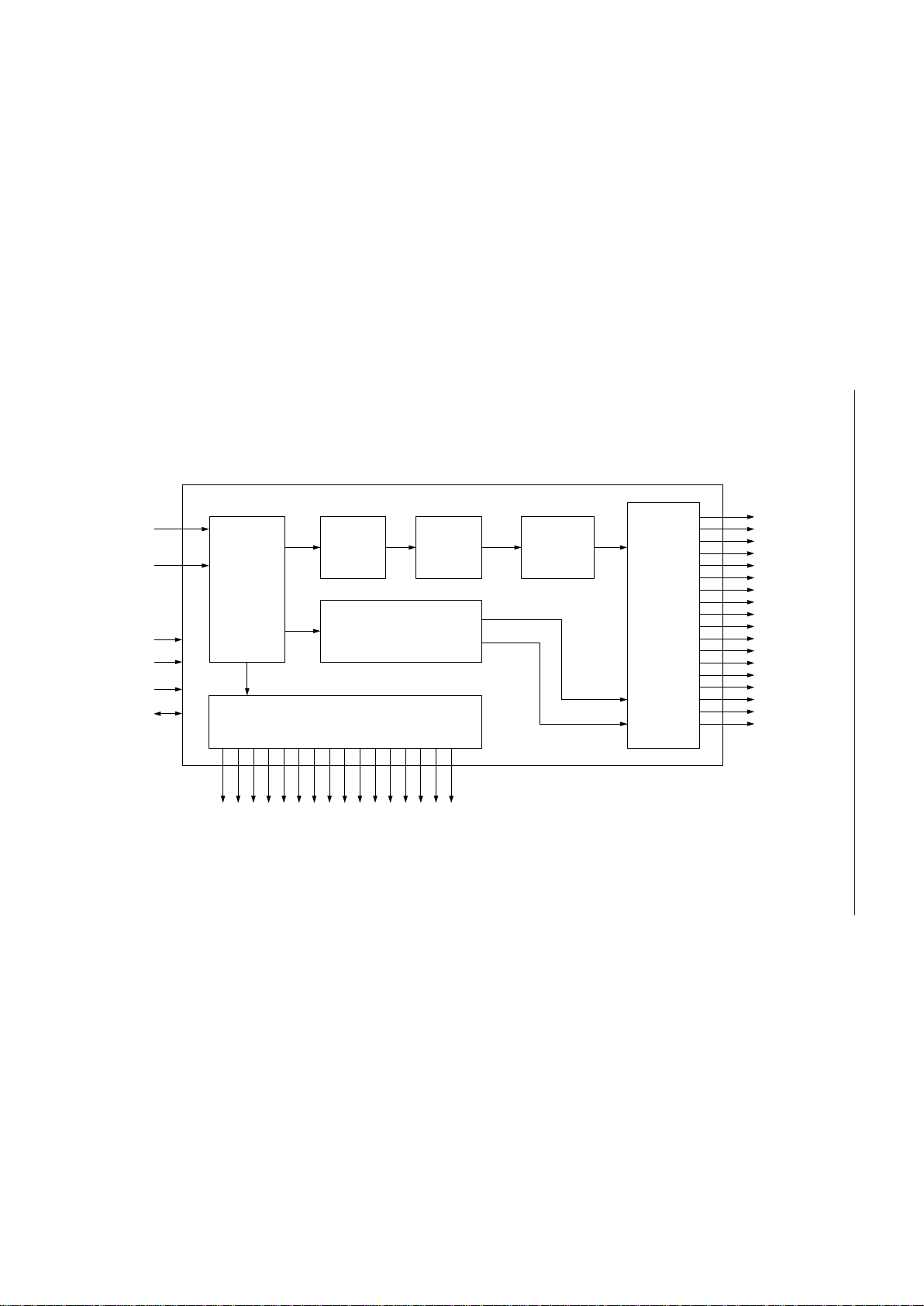
BLOCK DIAGRAM
SGA
SGB
SGC
SGD
SGE
SGF
SGG
SGH
SGI
SGJ
SGK
SGL
SGM
SGN
SGO
SGP
PNT
TAIL
AD16
AD15
AD14
AD13
AD12
AD11
AD10
AD 9
AD 8
AD 7
AD 6
AD 5
AD 4
AD 3
AD 2
AD 1
DATA
SCLK
POR
V
SS
V
DD
A
SEGMENT
DRIVERS
(ANODE)
SEGMENT
DECODER
64¥16
PLA
6¥16
DISPLAY
DATA
BUFFER
TIMING
AND
CONTROL
2¥16
DECIMAL PT.
COMMA TAIL
DIGIT DRIVERS
(GRID)
Page 3

¡ Semiconductor MSC1951-01
INPUT AND OUTPUT CONFIGURATION
• Schematic Diagrams of Logic Portion Input Circuit
V
SS
V
SS
INPUT
V
DD
• Schematic Diagrams of Logic Portion Output Circuit
V
SS
V
SS
V
DD
OUTPUT
V
DD
• Schematic Diagrams of Driver Output Circuit
V
SS
V
SS
V
DD
OUTPUT
3/17
Page 4
¡ Semiconductor MSC1951-01
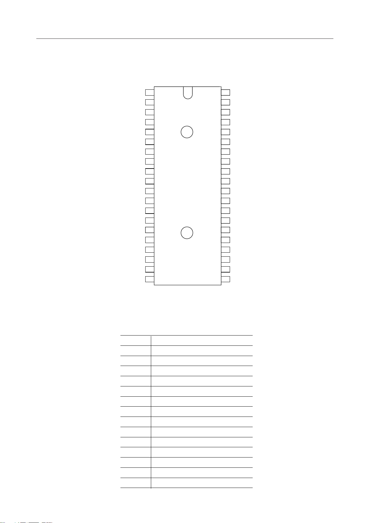
PIN CONFIGURATION (TOP VIEW)
V
DD
V
SS
AD16
AD15
AD14
AD13
AD12
AD11
AD10
AD 9
AD 8
AD 7
AD 6
AD 5
AD 4
AD 3
AD 2
AD 1
(GND)
POR
38
37
34
PNT
TAIL
SGP
SGO
SGN
SGM
SGL
SGK
SGJ
SGI
SGH
SGG
SGF
SGE
SGD
SGC
SGB
SGA
SCLK
DATA
140
239
3
4
536
635
7
833
932
10 31
11 30
12 29
13 28
14 27
15 26
16 25
17 24
18 23
A
19 22
20 21
40-Pin Plastic DIP
Pin No. Function
1 Power supply (5V)
2 Digit output pin 16
~
17 Digit output pin 1
18 GND
19 TEST pin
20 POWER-ON-RESET pin
21 Data input pin
22 Shift clock pin
23 Segment output pin A
~~
38 Segment output pin P
39 TAIL output pin
40 POINT output pin
~
4/17
Page 5
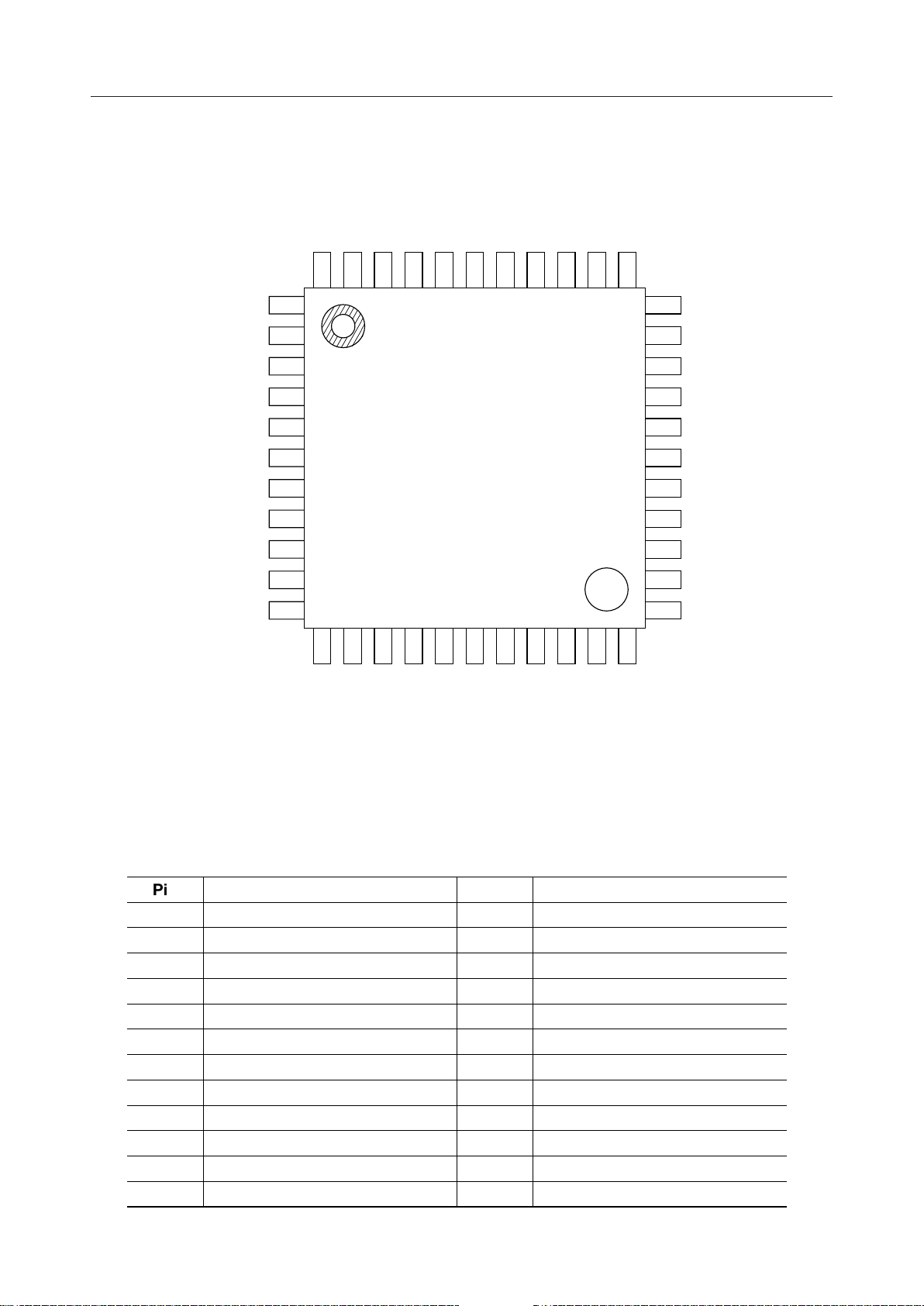
¡ Semiconductor MSC1951-01
(GND)
DD
SS
AD16
AD15
AD14
AD13
44
43
42
41
V
40
V
39
PNT
38
TAIL
37
SGP
36
SGO
35
SGN
34
NC
AD12
AD11
AD10
AD 9
AD 8
AD 7
AD 6
AD 5
AD 4
AD 3
10
11
1
2
3
4
5
6
7
8
9
22
21
20
19
18
17
16
15
14
13
12
AD 2
AD 1
(GND)
DD
V
A
POR
(GND)
DD
V
DATA
SCLK
SGA
SGB
NC
33
32
31
30
29
28
27
26
25
24
23
SGM
SGL
SGK
SGJ
SG I
SG H
SGG
SGF
SGE
SGD
SGC
Pin Function
1 No-connection pin
2 Digit output pin 12
~
~
13 Digit output pin 1
14 GND
15 TEST pin
16 POWER-ON-RESET pin
17 GND
18 Data input pin
19 Shift clock pin
20 Segment output pin A
21 Segment output pin B
NC : No-connection pin
44-Pin Plastic QFP
Pin Function
22 No-connection pin
23 Segment output pin C
~
36 Segment output pin P
37 TAIL output pin
38 POINT output pin
39 GND
40 Power supply (5V)
41 Digit output pin 16
~
44 Digit output pin 13
~
~
5/17
Page 6

¡ Semiconductor MSC1951-01
PIN DESCRIPTIONS
Symbol Type Description
V
SS
V
DD
DATA I
SCLK I
POR I
A I/O
AD16 to AD1 O
SGA to SGP
TAIL, PNT
—
—
Power supply pin
GND pin
Serial data Input of display data/control data
Input from MSB
Shift clock signal input of shift register
Shifts data at the falling edge of SCLK
Power-on-reset input. Input of "H" level into this pin with the power turned on
initializes this IC.
The internal state after the initialization is as follows:
1) AD1 to AD16, SGA to SGP, TAIL and PNT output are in the off state.
2) The duty cycle is set to "0".
3) The digit counter value is set to 16 digits.
4) The buffer pointer is set to AD1.
5) Pin "A" is in the output mode.
Usually used as an output mode, and outputs 1/5 of the internal oscillation
frequency. In the test mode, operates as an input pin.
Grid output pin
The output configuration is an emitter follower.
O
Segment output pin
The output configuration is an emitter follower.
6/17
Page 7

¡ Semiconductor MSC1951-01
ABSOLUTE MAXIMUM RATINGS
Parameter Symbol
Power Supply Voltage
Input Voltage
Output Voltage
V
SS
V
IN
V
SS
Digit
Output Current
I
LOAD
Segment
DIP
QFP
Storage Temperature °C–55 to 150T
STG
RECOMMENDED OPERATING CONDITIONS
Parameter Symbol
Power Supply Voltage
High Level Input Voltage
Low Level Input Voltage
Clock Frequency
OSC Frequency
Frame Frequency
Operating Temperature °CT
V
V
V
f
SS
IH
IL
f
C
OSC
f
FR
op
Condition Unit
—
All inputs
All inputs
—
—
—
—
Rating Unit
–0.3 to +6.5
–0.3 to V
V
– 58 to V
SS
SS
+ 0.3
SS +
0.3
–25
–20
–10
Min.
4.5
3.6
0.0
—
—
—
–40
Typ.
—
—
—
—
500
195
—
Max.
5.5
5.5
1.0
500
—
—
85
V
V
V
mA
mA
mA
V
V
V
kHz
kHz
Hz
7/17
Page 8

¡ Semiconductor MSC1951-01
ELECTRICAL CHARACTERISTICS
DC Characteristics
(VSS = 5 V±10%, VGG = –53 V±0.5 V, Ta = –40 to +85°C)
Parameter Symbol
High Level Input Voltage
Low Level Input Voltage
High Level Input Current
Low Level Input Current
V
IH
V
IL
I
IH
I
IL
V
OH1
Digit
High Level Output Voltage
V
OH2
Low Level Output Voltage
Output Leakage Current —
V
I
OUT
I
OL
SS
Segment
"L" output current is determined by
external pull-down resistor
Condition Unit
All inputs
All inputs
= V
V
IH
SS
VIL = 0.0 V
V
= 5 V
SS
I
= –10 mA
LOAD
V
= 5 V
DIP
QFP 2.5
V
= VSS – VGG = –53 V
OUT
I
LOAD
VSS = 5 V
I
LOAD
SS
= –10 mA
= –5mA
AC Characteristics
(V
= 5 V±10%, VGG = –53 V±0.5 V, Ta = –40 to +85°C)
SS
Parameter Symbol Condition Unit
Self-oscillation Frequency
Frame Frequency
Clock Frequency
SCLK "H" Time —t
SCLK "L" Time
Data Set-up Time
Data Hold Time
V
Rise Time
SS
POR Pulse Width
POR-SCLK Time
Internal Processing Time
f
OSC
f
f
CW-H
CW-L
t
DS
t
DH
t
PRZ
t
RESW
t
RESS
t
BUSY
FR
C
When unit mounted
—
—
—
—t
—
—
—
—
—
Min.
3.6
0.0
–2.0
–2.0
3.0
2.5
—
392
88
—
1.0
200
100
100
200
200
40
Max.
5.5
1.0
2.0
2.0
V
GG
10.0
10.0—Current Consumption
Max.Min.
548
332
500
—
—
—
+3.0
—
—1.0
—
—
—
—
—
—
V
V
mA
mA
V
V
V
V
mA
mANo load
kHz
Hz
kHz
ms
ms
ns
ns
ms
ms
ns
ms
8/17
Page 9

¡ Semiconductor MSC1951-01
TIMING DIAGAM
a) SCLK and Data Timing
t
BUSY
–3.6 V
SCLK
t
CW-HtCW-L
t
DS
t
DH
f
C
–1.0 V
DATA
b) VSS Input and Data Word Transfer Timing
V
SS
t
PRZ
POR
t
RESW
t
RESS
t
BUSY
–3.6 V
–1.0 V
–4.5 V
–0 V
SCLK
MSB side
Data Word
Data Word
LSB side MSB side LSB side
9/17
Page 10

¡ Semiconductor MSC1951-01
FUNCTIONAL DESCRIPTION
The MSB value of 8-bit serial data determines whether the input data into MSC1951-01 is control
data or display data.
Display Data
By setting MSB = "0", the display data can be entered. The address of PLA and set values are
specified by bit 5 to bit 0 following MSB.
Tables 1 to 3 provide the PLA code table.
Command
Display Data
Description
Set Display contents
MSB
bit7
bit6 bit5 bit4 bit3 bit2 bit1
0X2
5
4
2
3
2
2
2
1
2
LSB
bit0
2
0
X: Don't care
Control Data
The control data can be input by setting MSB to "1". In addition, a command type and set values
are determined by the bit 6 to bit 0 following MSB.
Command Function
Buffer Pointer Control
Digit Counter Control
Specifies the RAM
address.
Sets the number of
display digits.
Duty Cycle Control Sets the duty value.
Test Mode Sets the test mode.
MSB
bit 7
bit 6 bit 5 bit 4 bit 3 bit 2 bit 1
12
12
12
1X002
0102
1002
112
4
4
3
3
3
2
XXX
2
2
2
2
2
2
LSB
bit 0
1
2
1
2
1
2
0
0
0
X: Don't care
a) Buffer Pointer Control
This command changes the display contents only at an arbitrary digit. (The RAM write
address is set.)
To input data into bits 0 to 3, set (desired digit –2).
(Example) When specifying AD4, the set value is 2 (0010).
Specified Digit Set Value of
Bits 0 to 3
AD1
AD2
AD3
AD4
AD5
AD6
AD7
AD8
15 (1111)
0 (0000)
1 (0001)
2 (0010)
3 (0011)
4 (0100)
5 (0101)
6 (0110)
Specified Digit Set Value of
Bits 0 to 3
AD9
AD10
AD11
AD12
AD13
AD14
AD15
AD16
7 (0111)
8 (1000)
9 (1001)
10 (1010)
11 (1011)
12 (1100)
13 (1101)
14 (1110)
10/17
Page 11

¡ Semiconductor MSC1951-01
b) Digit Counter Control
This command sets the number of display digits.
Set the desired number of digits in bits 0 to 3.
Number of
Display Digits
1
2
3
4
5
6
7
8
Set Value of
Bits 0 to 3
1 (0001)
2 (0010)
3 (0011)
4 (0100)
5 (0101)
6 (0110)
7 (0111)
8 (1000)
Number of
Display Digits
9
10
11
12
13
14
15
16
Set Value of
Bits 0 to 3
9 (1001)
10 (1010)
11 (1011)
12 (1100)
13 (1101)
14 (1110)
15 (1111)
0 (0000)
c) Duty Cycle Control
This command sets the duty cycle of the driver output. This command allows the brightness
to be adjusted by 1/32 step. As shown in Figure 1, the blank time between digits or between
the segments is specified by 1 bit time on the hardware. Therefore, the set value ranges from
0 to 31.
1 DISPLAY CYCLE
512 bit times
AD1
AD2
AD3
AD4
AD5
AD6
AD7
AD8
AD9
AD10
AD11
AD12
AD13
AD14
AD15
AD16
SGn
31bit times
1 bit time
31bit times
1 bit time
V
SS
V
GG
V
SS
V
GG
Note: At the time of Duty Cycle = 31 (I bit time = 5 ¥ 1/fosc)
Fig. 1 Output Timing
11/17
Page 12

¡ Semiconductor MSC1951-01
d) Test Mode
This mode is not a user function, but is used for outgoing inspection.
Table 1 PLA Code Table
Input Code
7 6543210
0
X
0
0
0
0
0
0
0
0
0
0
0
0
0
0
0
0
0
0
0
0
0
0
0
0
0
0
0
0
0
0
0
0
0
0
0
1
0
1
0
1
0
1
0
1
0
1
0
1
0
1
0
1
0
1
0
1
0
1
0
1
0
1
0
1
0
1
1
0
1
0
1
0
1
0
1
0
1
0
1
0
1
0
1
0
1
0
1
0
1
0
1
0
1
0
1
0
1
0
1
1
1
1
1
1
1
1
1
1
1
1
1
1
1
1
1
1
1
1
1
1
1
1
1
1
1
1
1
1
1
1
0
0
0
0
0
0
0
1
0
1
0
1
0
1
1
0
1
0
1
0
1
0
1
1
1
1
1
1
1
1
0
0
0
0
0
0
0
0
0
1
0
1
0
1
0
1
1
0
1
0
1
0
1
0
1
1
1
1
1
1
1
1
0
0
0
0
0
0
0
0
0
1
0
1
0
1
0
1
1
0
1
0
1
0
1
0
1
1
1
1
1
1
1
1
0
0
0
0
0
0
0
0
0
1
0
1
0
1
0
1
1
0
1
0
1
0
1
0
1
1
1
1
1
1
1
1
0
0
1
1
0
0
1
1
0
0
1
1
0
0
1
1
0
0
1
1
0
0
1
1
0
0
1
1
0
0
1
1
0
0
1
1
0
0
1
1
0
0
1
1
0
0
1
1
0
0
1
1
0
0
1
1
0
0
1
1
0
0
1
1
0
X
0
X
0
X
0
X
0
X
0
X
0
X
0
X
0
X
0
X
0
X
0
X
0
X
0
X
0
X
X
0
X
0
X
0
X
0
X
0
X
0
X
0
X
0
X
0
X
0
X
0
X
0
X
0
X
0
X
0
X
0
X
0
X
0
X
0
X
0
X
0
X
0
X
0
X
0
X
0
X
0
X
0
X
0
X
0
X
0
X
0
X
0
X
0
X
0
X
0
X
0
X
0
X
0
X
0
X
0
X
0
X
0
X
0
X
0
X
0
X
0
X
0
X
0
Function
0
Segment A On
1
Segment B On
0
Segment C On
1
Segment D On
0
Segment E On
1
Segment F On
0
Segment G On
1
Segment H On
0
Segment I On
1
Segment J On
0
Segment K On
1
Segment L On
0
Segment M On
1
Segment N On
0
Segment O On
1
Segment P On
0
Segment A On
1
Segment A & B On
0
Segment A-C On
1
Segment A-D On
0
Segment A-E On
1
Segment A-F On
0
Segment A-G On
1
Segment A-H On
0
Segment A-I On
1
Segment A-J On
0
Segment A-K On
1
Segment A-L On
0
Segment A-M On
1
Segment A-N On
0
Segment A-O On
1
Segment A-P On
0
Number 0
1
Number 1
0
Number 2
1
Number 3
0
Number 4
1
Number 5
0
Number 6
1
Number 7
0
Number 8
1
Number 9
0
Letter P
1
Letter L
0
Comma
1
Blank
0
Decimal
1
Blank
0
Number 0
1
Number 1
0
Number 2
1
Number 3
0
Number 4
1
Number 5
0
Number 6
1
Number 7
0
Number 8
1
Number 9
0
Letter A
1
Letter B
0
Letter C
1
Letter D
0
Letter E
1
Letter F
Segment Driver Output Patterns (1 = On)
SGA SGB SGC SGD SGE SGF SGG SGH SGI SGJ SGK SGL SGM SGN SGO SGP
1
1
1
1
1
1
1
1
1
1
1
1
1
1
1
1
1
1
1
1
1
1
1
1
1
1
1
1
1
1
1
1
1
1
1
1
1
1
1
1
1
1
1
1
1
1
1
1
1
1
1
1
1
1
1
1
1
1
1
1
1
1
1
1
1
1
1
1
1
1
1
1
1
1
1
1
1
1
1
1
1
1
1
1
1
1
1
1
1
1
1
1
1
1
1
1
1
1
1
1
1
1
1
1
1
1
1
1
1
1
1
1
1
1
1
1
1
1
1
1
1
1
1
1
1
1
1
1
1
1
1
1
1
1
1
1
1
1
1
1
1
1
1
1
1
1
1
1
1
1
1
1
1
1
1
1
1
1
1
1
1
1
1
1
1
1
1
1
1
1
1
1
1
1
1
1
1
1
1
1
1
1
1
1
1
1
1
1
1
1
1
1
1
1
1
1
1
1
1
1
1
1
1
1
1
1
1
1
1
1
1
1
1
1
1
1
1
1
1
1
1
1
1
1
1
1
1
1
1
1
1
1
1
1
1
1
1
1
1
1
1
1
1
1
1
1
1
1
1
1
1
1
1
1
1
1
1
1
1
1
1
1
1
1
1
1
1
1
1
1
1
1
1
1
1
1
1
1
1
1
1
1
1
1
1
1
1
1
1
1
1
1
1
1
1
1
1
1
1
1
1
1
1
1
1
1
1
1
1
1
1
1
1
1
1
1
1
1
1
1
1
1
1
1
1
1
1
1
1
1
1
1
1
1
1
1
111
1
1
1
1
1
1
1
1
1
1
1
1
1
1
1
1
1
1
1
1
1
1
1
1
1
1
1
1
1
1
1
1
1
1
1
1
1
1
1
11
1
1
1
1
1
1
1
1
1
1
1
1
1
1
1
1
1
1
1
1
1
1
1
1
1
1
1
1
1
1
1
1
1
1
1
1
1
1
PNT TAIL
1
1
1
Any 1 of
16 Segments
Bargraph
Codes
1 to 16
Segments
Alphanumeric and
Special Codes
12/17
Page 13

¡ Semiconductor MSC1951-01
Table 2 PLA Code (At the time of 7-segment Display)
00
01
02
03
04
05
06
08 10
09 11 19 21 29 31 39
0A 12 1A 22 2A 32 3A
0B 13 1B 23 2B 33 3B
0C 14 1C 24 2C 34 3C
0D 15 1D 25 2D 35 3D
0E 16 1E 26 2E 36 3E
18
20 28 30 38
;
•
07
0F 17 1F 27 2F 37 3F
SGP
SGO
SGN
SGM
SGL
SGK
SGJ
SGI
SGH
SGG
SGF
SGE
SGD
SGC
SGB
SGA
16-SEGMENT
BARGRAPH
SGF SGB
SGE SGC
PNT
TAIL
SGA
SGG
SGD
7-SEGMENT
ALPHANUMERIC
13/17
Page 14

¡ Semiconductor MSC1951-01
Table 3 PLA Code (At the time of bar display)
00 01 02 03 04 05 06 07 08 09 0A 0B 0C 0D 0E 0F
7-SEGMENT
CHARACTERS
SPECIAL
BARGRAPH
CODES
7-SEGMENT
CHARACTERS
SPECIAL
BARGRAPH
CODES
7-SEGMENT
CHARACTERS
•
= PNT and TAIL both set
••
= PNT only set
SPECIAL
BARGRAPH
CODES
SGP
SGO
SGN
SGM
SGL
SGK
SGJ
SGI
SGH
SGG
SGF
SGE
SGD
SGC
SGB
SGA
SGP
SGO
SGN
SGM
SGL
SGK
SGJ
SGI
SGH
SGG
SGF
SGE
SGD
SGC
SGB
SGA
SGP
SGO
SGN
SGM
SGL
SGK
SGJ
SGI
SGH
SGG
SGF
SGE
SGD
SGC
SGB
SGA
SEE FIGURE 2
10 11 12 13 14 15 16 17 18 19 1A 1B 1C 1D 1E 1F
SEE FIGURE 2
••
20 21 22 23 24 25 26 27 28 29 2A 2B 2C 2D 2E 2F
0123456789PL
*
SGP
SGO
SGN
SGM
SGL
SGK
SGJ
SGI
SGH
SGG
SGF
SGE
SGD
SGC
SGB
SGA
30 31 32 33 34 35 36 37 38 39 3A 3B 3C 3D 3E 3F
0123456789ABCDEF
7-SEGMENT
CHARACTERS
SPECIAL
BARGRAPH
CODES
14/17
Page 15

¡ Semiconductor MSC1951-01
* To set the comma and point, the display data at the display digit is input, then 2C and 2E data
are input.
Note: Only when 2C and 2E data are entered, the write address in the RAM is not automatically
incremented. For other data, the address specified by the Buffer Pointer Control
command is automatically incremented by one each time the display data is input.
APPLICATION CIRCUIT
+5V
10mF
V
DD
V
SS
MSC1951-01
DATA
SCLK
DATA
CLOCK
HOST
SYSTEM
ADn SGn POR
16 16
TYPICAL
GRID
(DIGIT)
R
C
DRIVER
CIRCUIT
R
G
E
K
TYPICAL
ANODE
(SEGMENT)
DRIVER
CIRCUIT
R
A
VACUUM
FLUORESCENT
DISPLAY
–V
GG
15/17
Page 16

¡ Semiconductor MSC1951-01
PACKAGE DIMENSIONS
(Unit : mm)
DIP40-P-600-2.54
Package material
Lead frame material
Pin treatment
Solder plate thickness
Package weight (g)
Epoxy resin
42 alloy
Solder plating
5 mm or more
6.10 TYP.
Notes for Mounting the Surface Mount Type Package
The SOP, QFP, TSOP, SOJ, QFJ (PLCC), SHP and BGA are surface mount type packages, which
are very susceptible to heat in reflow mounting and humidity absorbed in storage.
Therefore, before you perform reflow mounting, contact Oki’s responsible sales person for the
product name, package name, pin number, package code and desired mounting conditions
(reflow method, temperature and times).
16/17
Page 17

¡ Semiconductor MSC1951-01
(Unit : mm)
QFP44-P-910-0.80-K
Mirror finish
Package material
Lead frame material
Pin treatment
Solder plate thickness
Package weight (g)
Epoxy resin
42 alloy
Solder plating
5 mm or more
0.35 TYP.
Notes for Mounting the Surface Mount Type Package
The SOP, QFP, TSOP, SOJ, QFJ (PLCC), SHP and BGA are surface mount type packages, which
are very susceptible to heat in reflow mounting and humidity absorbed in storage.
Therefore, before you perform reflow mounting, contact Oki’s responsible sales person for the
product name, package name, pin number, package code and desired mounting conditions
(reflow method, temperature and times).
17/17
 Loading...