

Page 1

E2C0024-27-Y4
¡ Semiconductor
This version: Nov. 1997
Previous version: Jul. 1996
MSC1230¡ Semiconductor
MSC1230
111-Bit 2/3-Duty Controller/Driver with Digital Dimming Function
GENERAL DESCRIPTION
The MSC1230 is a Bi-CMOS display driver with digital dimming function. It enables switching
between 1/3-duty vacuum fluorescent (VF) display tube and universal VF display tube by pin
control.
The MSC1230 consists of a 112-bit shift register, a 111-bit latch, a 10-bit digital dimming circuit,
37 segment drivers, and 3 grid drivers.
The MSC1230 provides an interface with a microcomputer only by three signal lines: CS,
DATA-IN, and CLOCK.
By using the chip select function, the DATA-IN and CLOCK signal lines can be shared
by other peripheral circuits.
FEATURES
• Power supply voltage :
• Operating temperature range : Ta=–40 °C to +85 °C
• 37-segment driver outputs : IOH=–6 mA at VOH = VDD –0.8 V
• 3-grid driver outputs : IOH=–30 mA at VOH = VDD –0.8 V
• Built-in digital dimming circuit (10-bit resolution)
• Switchable between 1/3-duty VF display tube and universal VF display tube*
When SEL pin is left open : Selects universal VF display tube (The grids GRID1, GRID2,
and GRID1+GRID2 are turned on repeatedly in this order)
When SEL pin is used at 0 V : Selects 1/3-duty VF display tube (The grids GRID1, GRID2,
and GRID3 are turned on repeatedly in this order)
• Built-in oscillation circuit (external R and C)
• Built-in Power-On-Reset circuit
• Package:
56-pin plastic QFP (QFP56-P-910-0.65-2K)(Product name: MSC1230GS-2K)
* A universal VF display tube is a display tube for which, like a gate array, the user can freely
design characters and patterns on the master layer (grid). (Pattern can be created without gaps
between grids.)
Since the outline dimensions of the display tube and the grid layout are predetermined,
desired patterns can be displayed in a short time.
The universal VF display tube is used for the display parts for audio equipment, household
appliances, and automobile equipment.
VDD=8 V to 18 V (built-in 5 V regulator for logic circuit)
1/13
Page 2
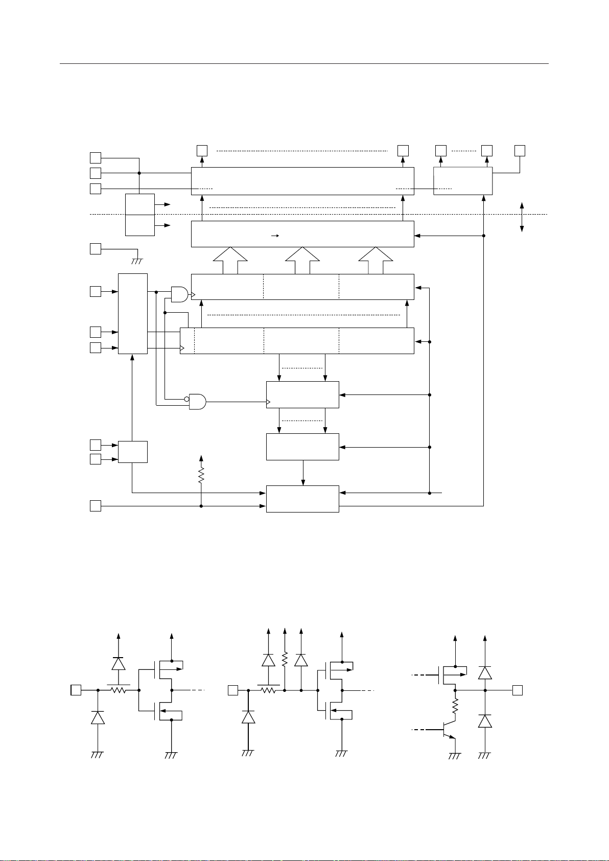
BLOCK DIAGRAM
MSC1230¡ Semiconductor
V
DD1
V
DD2
DGND
LGND
CS
DATA-IN
CLOCK
OSC0
OSC1
5V
REG.
POR
Control
Circuit
OSC
SEG37 SEG1 GRID3 GRID1
37-bit Segment Driver
5V
POR
37
75111 74 38 37 1
112 111 107106 97 96
5V
37bit data
111 37-Segment Control
3737
111-bit Latch
111-bit data
112-bit Shift Register
10-bit data
10-bit Latch
10-bit data
10-bit Digital
Diming
1
37
3-bit Grid Driver
1
V
3
DD
V
=8 - 18V
DD
VCC=5.0V
(Regurator)
SEL
112bits=0: Digital Dimming Mode
112bits=1: VF Data Input Mode
INPUT AND OUTPUT CONFIGURATION
l Schematic Diagram 1 of
Logic Portion Input Circuit
(5V Reg.)
GND
INPUT
V
DD
GND
l Schematic Diagram 2 of
Logic Portion Input Circuit
V
DD
COLn
GND
Timing
Generator
(5V Reg.)
GND
POR
l Schematic Diagram of
Driver Output Circuit
V
GND
DD
V
DD
OUTPUT
GND
2/13
Page 3
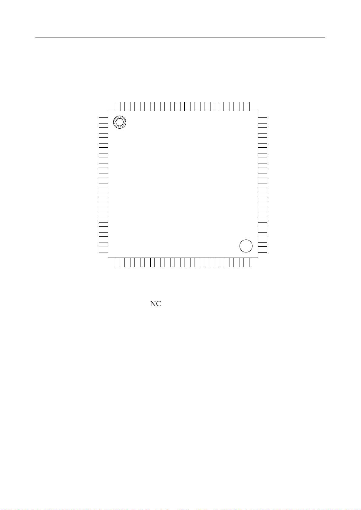
PIN CONFIGURATION (TOP VIEW)
MSC1230¡ Semiconductor
SEG19
SEG20
SEG21
SEG22
SEG23
SEG24
SEG25
SEG26
SEG27
SEG28
SEG29
10
11
SEG30 12
SEG31 13
SEG32 14
SEG17
SEG18
55
56
SEG15
SEG16
53
54
DD2
V
SEG14
51
52
NC
50
DGND
49
1
2
3
4
5
6
7
8
9
22
21
20
15
16
17
18
19
NC
48
23
DD1
V
47
24
SEG13
SEG1245
46
25
26
SEG1144
27
SEG1043
28
42
41
40
39
38
37
36
35
34
33
32
31
30
29
SEG9
SEG8
SEG7
SEG6
SEG5
SEG4
SEG3
SEG2
SEG1
NC
GRID1
GRID2
GRID3
V
DD3
SEG34
SEG33
NC
SEG36
SEG35
SEG37
LGND
NC: No connection
56-Pin Plastic QFP
NC
OSC1
OSC0
SEL
CS
CLOCK
DATA-IN
3/13
Page 4

PIN DESCRIPTION
MSC1230¡ Semiconductor
Pin
34 to 46,
Symbol Type Decription
SEG1 to 37 O Output pins for segment signals for driving VF display tube.
52 to 56,
1 to 19
30 to 32
25
GRID1 to 3 O Output pins for grid signals for driving VF display tube.
SEL I When at a "L" level, this pin selects 1/3-duty VF display tube.
28
27
24
23
26
47
51
29
49 —
21 —
CLOCK
OSC0
OSC1
CS
V
DD1
V
DD2
V
DD3
DGND
LGND
The GRID3 output is not used when the universal VF display tube is used.
When at a "H" level (or when used in the open state), this pin selects universal
VF display tube.
IDATA-IN
Pin for series data input from microprocessor.
Data is input to the shift register on the rising edge of the CLOCK signal.
I
Serial clock input pin.
Data is input through the DATA-IN pin at the rising edge of the serial clock.
RC oscillator connecting pins.
I
Connect a resistor between the OSC1 and OSC0 pins and a capacitor between
O
the OSC0 pin and the ground.
I
Chip select input pin. Circuit operation is valid when this pin is at a "L" level.
Power supply pins. When using these pins, connect each of them to the power
—
supply.
Ground pins for driver and logic. These pins can be connected with each other
when they are used.
4/13
Page 5

ABSOLUTE MAXIMUM RATINGS
MSC1230¡ Semiconductor
Parameter
Supply Voltage
Input Voltage
Storage Temperature
Power Dissipation
Symbol Condition
V
DD
V
IN
T
STG
P
D
—
All inputs
—
Ta=85°C
RECOMMENDED OPERATING CONDITIONS
Parameter
Supply Voltage
High Level Input Voltage (1)
High Level Input Voltage (2)
Low Level Input Voltage (1)
Low Level Input Voltage (2)
Clock Frequency
Oscillation Frequency
Frame Frequency
Operating Temperature
V
V
V
V
V
f
OSC
f
T
DD
IH1
IH2
IL1
IL2
f
FR
op
All inputs except OSC0
All inputs except OSC0
C
R=4.7 kW, C=10 pF
f
OSC
—
OSC0
OSC0
—
=3.2 MHz
—
Ratings Unit
–0.3 to +20
–0.3 to +6.0
–65 to +150
400
V
V
°C
mW
Min. Typ. Max.Symbol Condition Unit
8
3.8
4.5
0.0
0.0
—
—
—
–40
—18
—
—
—
—
—
3.2
260
—
5.5
5.5
0.8
0.5
250
—
—
85
V
V
V
V
V
V
kHz
MHz
Hz
°C
5/13
Page 6

ELECTRICAL CHARACTERISTICS
DC Characteristics
Parameter
MSC1230¡ Semiconductor
(Ta=–40 to +85°C, VDD=8 to 18V)
Min. Max.Symbol Condition Unit
"H" Input Voltage (1) *1
"H" Input Voltage (2) *2
"L" Input Voltage (1) *1
"L" Input Voltage (2) *2
"H" Input Current (1) *3
"H" Input Current (2) *4
"L" Input Current (1) *3
"L" Input Current (2) *4
"H" Output Voltage (1) *5
"H" Output Voltage (2) *6
"L" Output Voltage *7
Supply Current
V
V
V
V
mA
mA
mA
mA
V
V
V
V
V
mA
VIH=5 V
V
IH
V
IL
V
IL
V
DD
I
OH1
V
DD
I
=–30 mA
OH2
V
DD
I
=500 mA
OL1
V
DD
I
=200 mA
OL2
V
DD
I
OL3
f
=3.2 MHz
osc
no Load
—
—
—
—
=5 V
=0 V
=0 V
=9.5 V
=–6 mA
=9.5 V
=9.5 V
=9.5 V
=9.5 V
=2 mA
3.8
4.5
0.0
0.0
–5
–200
–5
–0.6
V
DD
–0.8
V
DD
–0.8
—
—
—
—
V
IH1
V
IH2
V
IL1
V
IL2
I
IH1
I
IH2
I
IL1
I
IL2
V
OH1
V
OH2
V
OL1
V
OL2
V
OL3
I
DD
5.5
5.5
0.8
0.5
5
200
5
–0.1
—
—
2
1
0.3
13
*1 All input pins except OSC0
*2 OSC0 pin
*3 CS, CLOCK and DATA-IN pins
*4 SEL pin
*5 SEG1 to SEG37 pins
*6 GRID1 to GRID3 pins
*7 SEG1 to SEG37 and GRID1 to GRID 3 pins
6/13
Page 7

AC Characteristics
MSC1230¡ Semiconductor
Parameter
Oscillation Frequency
External Input Frequency
into OSC0
Clock Frequency
Clock Pulse Width
DATA Setup Time
DATA Hold Time
CS Pulse Width
CS Off Time
CS Setup Time
CS-Clock Time
CS Hold Time
Clock-CS Time
f
OSC
f
OSCI
f
t
CW
t
DS
t
DH
t
CSW
t
CSL
t
CSS
t
CSH
(Ta=–40 to +85°C, V
=8 to 18V)
DD
Min. Max.Symbol Condition Unit
R=4.7 kW , C=10 pF
2 4.4
MHz
External input only 2.7 3.7 MHz
C
—
—
—
—
—
—
—
—
1.3
1
200
8—
32
2
2
250
—
—
—
—
—
—
—
kHz
ms
ms
ns
ms
ms
ms
ms
CS-All Data Output Delay
Slew Rate (All Drivers)
CS Time at Power-on
Hold Time at Power-off
Rise Time at Power-on
ODS
t
PCS
t
POF
t
PRZ
C
=100 pFt
I
t
R
t=20% to 80% or 80% to 20%
CI=100 pF
—
When monuted on the unit
V
=0.0 V
DD
When monuted on the unit
—8
—
300
5
—
5
—
—
100 ms
ms
ms
ms
ms
7/13
Page 8

MSC1230¡ Semiconductor
CS
CLOCK
DATA-IN
CS
SEG1-37
GRID1-3
t
ODS
t
css
t
DStDH
t
R
t
csw
f
c
t
cw
t
DStDH
Figure 1. Data Input Timing
t
CSW
t
t
cw
ODS
t
DStDH
VALIDVALIDVALID
t
t
CSH
R
t
CSL
3.8V
0.8V
3.8V
0.8V
3.8V
0.8V
3.8V
0.8V
80%
20%
V
DD1, 2, 3
CS
Figure 2. SEG or GRID Driver Output Timing
t
t
PCS
t
POF
PRZ
Figure 3. Power-on Timing
8V
0V
3.8V
0.8V
8/13
Page 9

MSC1230¡ Semiconductor
FUNCTIONAL DESCRIPTION
Power-on Reset
When power is turned on, the IC is initialized by the internal power-on reset circuit. The status
of the internal circuit after initialization is as follows:
– The contents of the shift registers and latches are set to "0".
– The digital dimming duty cycle is set to "0".
Data Input
Data input to the DATA-IN pin is valid only when the CS pin is at a "L" level.
The input data to DATA-IN is shifted into the shift registers on the rising edge of the clock. The
data is automatically loaded to the latches on the rising edge of the CS pin.
When M0 = "1", the IC enters the display data input mode and a total of 112 bits of data are input.
When M0 = "0", the IC enters the digital dimming data input mode and a total of 16 bits of data
are input.
[Data Format]
1) Display Data Input Mode
Input Data : 112 bits
VF Display Data : 111 bits
Mode Select Data (M0) : 1 bit
112M0111
Mode
Data
(1 bit)
D111
110
D110
....
....97D9796D9695D9594D9493D9392D9291D91
Display Data (111 bits)
....
....4D43D32D21D1
2) Bit correspondence between segment outputs and shift registers
37363534333231302928272625242322212019181716151413121110987654321
37363534333231302928272625242322212019181716151413121110987654321
BIT
74 73 72 71 70 69 68 67 66 65 64 63 62 61 60 59 58 57 56 55 54 53 52 51 50 49 48 47 46 45 44 43 42 41 40 39 38
109 108 107 106 105 104 103 102 101 100111 110
99 98 97 96 95 94 93 92 91 90 89 88 87 86 85 84 83 82 81 80 79 78 77 76 75
First inBit
SEG
G1
G2
G3
9/13
Page 10

3) Input Format for VF data
Byte c7 c6 c5 c4 c3 c2 c1 c0
1 D8D7D6D5D4 D2
2 D16
3 D24
4 D32
5 D40
6 D48
7 D56
8 D64
9 D72
10 D80
11 D88
12 D96
13 D104
14 M0
D15
D23
D31
D39
D47
D55
D63
D71
D79
D87
D95
D103
D111
D14
D22
D30
D38
D46
D54
D62
D70
D78
D86
D94
D102
D110
D13
D21
D29
D37
D45
D53
D61
D69
D77
D85
D93
D101
D109
D12
D20
D28
D36
D44
D52
D60
D68
D76
D84
D92
D100
D108
D3
D11
D19
D27
D35
D43
D51
D59
D67
D75
D83
D91
D99
D107
D10
D18
D26
D34
D42
D50
D58
D66
D74
D82
D90
D98
D106
MSC1230¡ Semiconductor
D1
D9
D17
D25
D33
D41
D49
D57
D65
D73
D81
D89
D97
D105
4) Digital Dimming Data Input Mode
This data consists of 10 bits.
The output duty changes in the range of 0/1024 (0%) to 1016/1024 (99%) for each grid.
The 10-bit digital dimming data is input from the LSB.
Input Data : 16 bits
Digital Dimming Data : 10 bits
Mode Select Data : 1 bit
112M0111xx110xx109xx108xx107xx10610105910481037102610151004993982971First inBit
Mode
Data
(1bit)
(MSB) INPUT DATA (LSB)
0000000000
0000000001
1111111000
MSB LSB
Dimming Data (10 bits)
DUTY CYCLE
0/1024
1/1024
1016/1024
1111111111
1016/1024
10/13
Page 11

5) Input Format for Dimming Data
Byte c7 c6 c5 c4 c3 c2 c1 c0
1 87654 2
2M0xx xx xx xx
6) Function Mode
M0 FUNCTION
0 Display Data Input Mode
1 Digital Dimming Data Input Mode
GRID/SEG Driver Operation and Digital Dimming
3
xx 10
MSC1230¡ Semiconductor
1
9
Figures 4 and 5 show the timing for the GRID and SEG drivers in universal VFD mode and
1/3 duty VFD mode, respectively.
Figure 6 shows an example of timing for digital dimming operation in 1/3 duty VFD mode.
(When the duty cycle in the dimming data is 508/1024)
GRID1
3072 bit time
GRID2
GRID3
SEG1-37
* 1 bit time=4/f
(1 display cycle)
3 bit time
1019 bit time 1024 bit time
OSC
5 bit time 8 bit time
Figure 4. Duty Cycle Timing (Universal VFD Mode)
11/13
Page 12

GRID1
GRID2
GRID3
SEG1-37
3072 bit time
(1 display cycle)
3 bit time
1019 bit time 1024 bit time
5 bit time 8 bit time
Figure 5. Duty Cycle Timing (1/3 Duty Mode)
508 508
MSC1230¡ Semiconductor
GRID1
GRID2
GRID3
SEG1-37
3072 bit time
511 508 1024
Figure 6. Duty Cycle Timing (1/3 Duty Mode)
(When digital dimming data is changed from 3F8H to 1FFH)
≠≠
1016 bit time 511 bit time
12/13
Page 13

PACKAGE DIMENSIONS
QFP56-P-910-0.65-2K
Mirror finish
MSC1230¡ Semiconductor
(Unit : mm)
Package material
Lead frame material
Pin treatment
Solder plate thickness
Package weight (g)
Epoxy resin
42 alloy
Solder plating
5 mm or more
0.43 TYP.
Notes for Mounting the Surface Mount Type Package
The SOP, QFP, TSOP, SOJ, QFJ (PLCC), SHP and BGA are surface mount type packages, which
are very susceptible to heat in reflow mounting and humidity absorbed in storage.
Therefore, before you perform reflow mounting, contact Oki’s responsible sales person for the
product name, package name, pin number, package code and desired mounting conditions
(reflow method, temperature and times).
13/13
 Loading...