

Page 1

E2C0021-27-Y3
¡ Semiconductor MSC1212-01
¡ Semiconductor
This version: Nov. 1997
Previous version: Jul. 1996
MSC1212-01
48-Bit Grid/Anode Driver
GENERAL DESCRIPTION
The MSC1212-01 is a driver IC for VFD implemented in BiCMOS technology.
The circuit consists of a 48-bit shift register and a 48-bit latch; they control display data, which
is output from the display drivers.
Since a 64-pin plastic QFP package is used, the display unit size can be reduced.
FEATURES
• Logic supply voltage (VCC) : 4.5 to 5.5 V
• Driver supply voltage (V
• Operating temperature range : –40 to +105°C
• Driver output current : I
• Built-in 48-bit output Driver (with latch)
• Built-in 48-bit shift register
• Clock frequency : 0.5 MHz
• Package:
64-pin plastic QFP (QFP64-P-1414-0.80-BK) (Product name: MSC1212-01GS-BK)
) : 8 to 18 V
DISP
= –6 mA (for only one driver on state)
O2-1
I
= –50 mA (total current for all drivers on
O2-2
state)
I
= 0.2 mA
O2-3
1/11
Page 2
¡ Semiconductor MSC1212-01
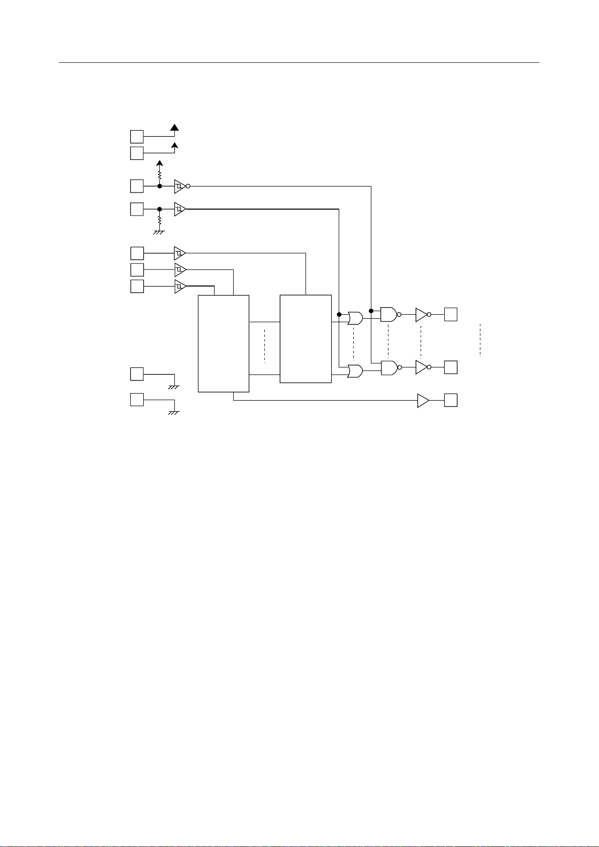
BLOCK DIAGRAM
V
DISP
V
CC
CL
CHG
LS
DIN
CLK
L-GND
D-GND
V
CC
CSI
PO1
48-BIT
S/R
PO48
L
I1 O1
48-BIT
LATCH
O48I48
HVO 1
HVO48
SO
DOUT
2/11
Page 3
¡ Semiconductor MSC1212-01
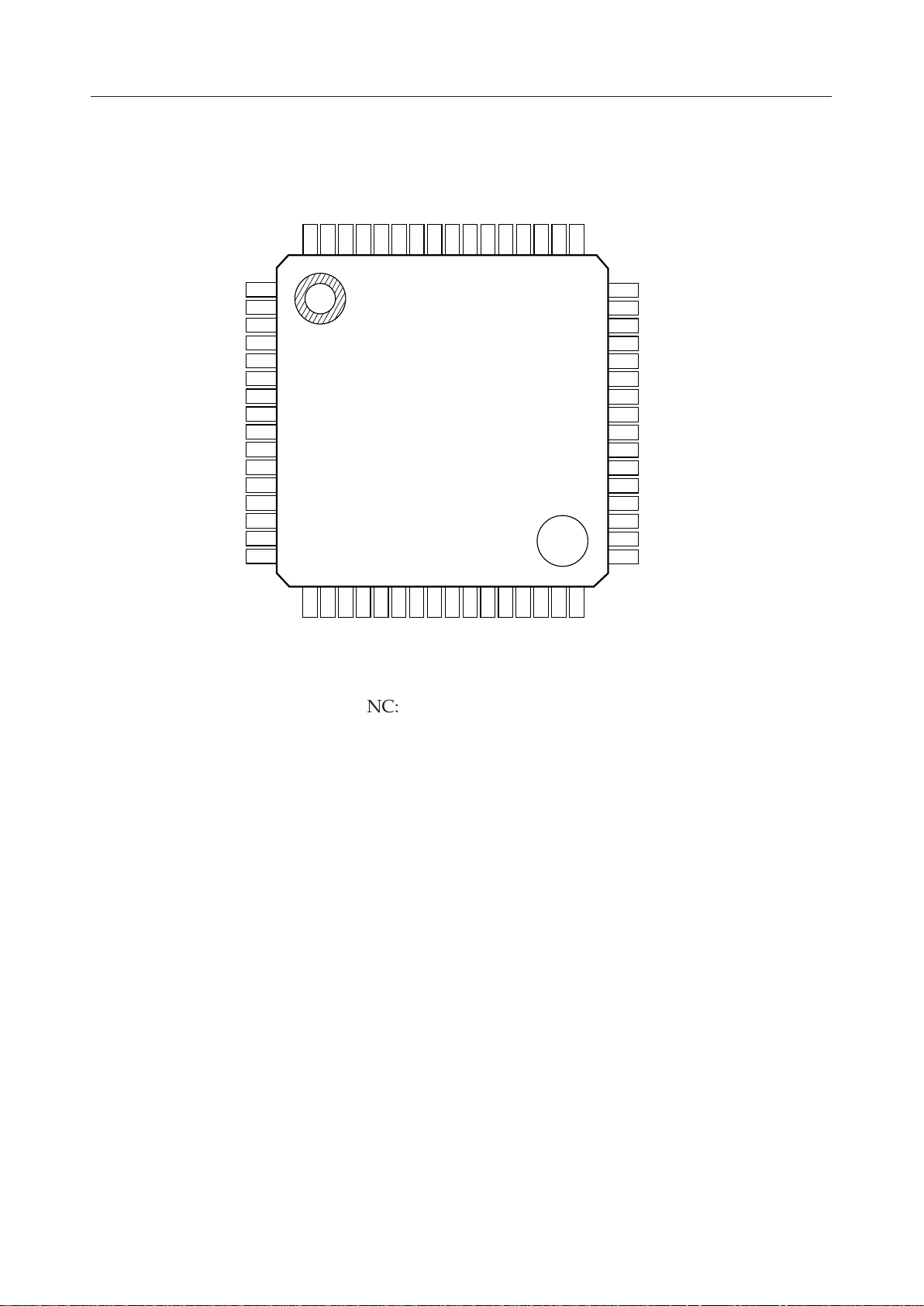
PIN CONFIGURATION (TOP VIEW)
NC
HVO 18
HVO 19
HVO 20
HVO 21
HVO 22
HVO 23
HVO 24
HVO 25
HVO 26
HVO 27
HVO 28
HVO 29
HVO 30
HVO 31
NC
HVO 17
HVO 16
HVO 15
HVO 14
HVO 13
HVO 12
HVO 11
HVO 10
HVO 9
HVO 8
HVO 7
HVO 6
HVO 5
HVO 4
HVO 3
HVO 2
10
11
12
13
14
15
16
646362616059585756555453525150
1
2
3
4
5
6
7
8
9
171819202122232425262728293031
DISP
HVO1NCV
D-GND
L-GND
DIN
CLKLSCL
CHG
VCCDOUT
D-GND
DISP
V
NC
49
32
HVO 48
48
47
46
45
44
43
42
41
40
39
38
37
36
35
34
33
HVO 32
HVO 33
HVO 34
HVO 35
HVO 36
HVO 37
HVO 38
HVO 39
HVO 40
HVO 41
HVO 42
HVO 43
HVO 44
HVO 45
HVO 46
HVO 47
NC: No-connection pin
64-Pin Plastic QFP
3/11
Page 4
¡ Semiconductor MSC1212-01
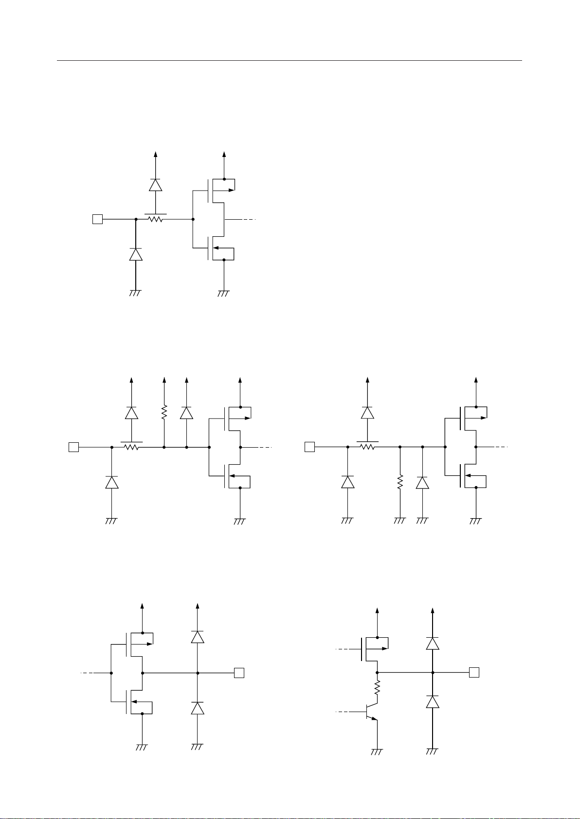
INPUT AND OUTPUT CONFIGURATION
• Schematic Diagrams of Logic Portion Input Circuit
V
DISP
V
CC
INPUT
GND
GND
• Schematic Diagrams of Logic Portion Input
Circuit (Pull-up)
V
DISP
V
CC
• Schematic Diagrams of Logic Portion Input
Circuit (Pull-down)
V
DISP
V
CC
INPUT
GND
GND
• Schematic Diagrams of Logic Portion Output
Circuit
V
CC
V
CC
OUTPUT
INPUT
GND
GND
• Schematic Diagrams of Driver Output Circuit
V
DISP
V
DISP
OUTPUT
GND
GND
GND
GND
4/11
Page 5

¡ Semiconductor MSC1212-01
PIN DESCRIPTION
Function
Driver Output
Driver Power Supply
Logic Power Supply
Driver GND
Logic GND
Data Input
Clock Input
Latch Strobe Input
Pin
1 to 17
32 to 48
50 to 63
19, 30
27
20, 29
21
22
23
24
Symbol
HVO1
to
HVO48
V
DISP
V
CC
D-GND
L-GND
DIN
CLK
LS
Description
Driver output pins, applicable to each bit of shift
register.
Power supply pins for driver circuit. Both Pin 19
and 30 should be connected externally.
Power supply pin for logic.
GND pins for the driver circuit.
Both Pin 20 and 29 should be connected externally.
GND pin for the logic circuit.
Input pin without pull-up or pull-down resistor.
Input pin of shift register. Display data input is
synchronized with clock signal. (positive logic)
Input pin without pull-up or pull-down resistor.
Data of shift register is shifted from one stage to
the next on application of each clock rising edge.
Input pin without pull-up or pull-down resistor.
When LS is at "H" level, the latch is shunted and the
shift register output becomes the lacth output.
When LS is at "L" level, the lacth holds the shift
register output just bafore LS goes to "L" level.
Clear Input
Test Input
Clear input pin with pull-up resistor. Normally "L"
25
26
28 DOUTData Output Serial output pin of shift register.
CL
CHG
level. In this condition, driver output changes to "H"
or "L" according to latch output level. When CL is
"H", all driver output pins are fixed to "L".
Test input pin with pull-down resistor. Normally "L"
level, but here, if CL="H", then driver output changes
to "H" or "L" according to latch output level.
If CL = "L" when CHG is at "H" level, all driver output
is fixed to "H" for test.
5/11
Page 6

¡ Semiconductor MSC1212-01
ABSOLUTE MAXIMUM RATINGS
Parameter Symbol
Logic Supply Voltage
Driver Supply Voltage
Input Voltage
Data Output Voltage
Driver Output Voltage
Power Dissipation
Thermal Resistance
Storage Temperature
*1
*1, *2
*1
*1
*1
*3
V
V
V
V
T
CC
DISP
V
IN
O1
O2
P
R
j-a
STG
D
Condition
—
—
—
Rating Unit
–0.3 to +6.5 V
–0.3 to +20 V
–0.3 to V
–0.3 to V
–0.3 to V
CC
CC
DISP
+0.3 VApplicable to all input pins
+0.3 VApplicable to data output pin
+0.3 VApplicable to driver output pin
1.0 WTa £ 25°C
120 °C/W
–55 to +150 °C—
*1 Maximum supply voltage with respect to L-GND and D-GND
*2 Catastrophic breakdown may occur if the applied voltage is more than the rating.
*3 Thermal resistance of package (between junction and atmosphere)
The junction temperature (T
Tj = P ¥ R
+ Ta (P is the maximum power dissipation)
j-a
) given by the following formula should not exceed 150°C.
j
6/11
Page 7

¡ Semiconductor MSC1212-01
RECOMMENDED OPERATING CONDITIONS
Parameter Symbol
Logic Supply Voltage
Driver Supply Voltage
High Level Input Voltage Applicable to all input pins
Low Level Input Voltage
Logic Output Current Applicable to DOUT pin
Driver High Level Output Current Only one driver is ON state
Driver High Level Output Current
Driver Low Level Output Current Applicable to all driver output pins
CLK Frequency See Timing Diagram
Data Setup Time See Timing Diagram
Data Hold Time See Timing Diagram
LS Pulse Width See Timing Diagram
CHG Pulse Width See Timing Diagram
CL Pulse Width See Timing Diagram
CLK Pulse Width See Timing Diagram
CLK-LS Delay Time See Timing Diagram
LS-CLK Delay Time See Timing Diagram
LS-CHG Delay Time See Timing Diagram
LS-CL Delay Time See Timing Diagram
Operating Temperature —
V
CC
V
DISP
V
IH
V
I
O1
I
O2-1
I
O2-2
I
O2-3
f
CLK
t
DS
t
DH
t
WLS
t
WCHG
t
WCL
t
WCLK
t
DCLK-LS
t
LS-CLK
W
t
WLS-CHG
t
WLS-CL
T
op
Applicable to logic supply voltage pin
Applicable to driver supply voltage pin
Applicable to all input pins
IL
Total current at all driver outputs
are ON state
Condition
Min. Unit
4.5
8
0.8 V
—
–0.1
—
—
—
—
400
300
125
10
10
500
525
0
0
0
–40
CC
Max.
5.5
18
—
0.2 V
0.1
–6
–50
0.2
0.5
—
—
—
—
—
—
—
—
—
—
105
CC
MHz
V
V
V
V
mA
mA
mA
mA
ns
ns
ns
ms
ms
ns
ns
ns
ns
ns
°C
7/11
Page 8

¡ Semiconductor MSC1212-01
ELECTRICAL CHARACTERISTICS
DC Characteristics
Parameter Symbol
Logic Power Supply
Current
Driver Power Supply
Current
High Level Input
Threshold Voltage
Low Level Input
Threshold Voltage
Hysteresis Voltage
High Level Input
Current
Low Level Input
Current
High Level Data
Output Current
Low Level Data
Output Current
Driver High Level
Output Current
Driver Low Level
Output Current
Voltage Difference
Between GND Pins
I
I
I
DISP
V
V
I
I
I
I
I
OH1
I
OL1
I
OH2
I
OL2
V
CC1
No Load
CC2
No Load
V
All input pins
P
All input pins
N
All input pins
H
IH1
IH2
IL1
IL2
= V
V
I
VI = 0V
V
V
–
CC
V
OL1
=
CC
OH1
1.0 V
1.0 V
=
Only one driver is ON state
V
DISP–VOH2
V
OL2
Voltage difference between
GND
= 1.0 V
1.0 V
=
D-GND and L-GND
= 4.5 to 5.5 V, V
(V
CC
Condition
f
= 0 Hz
CLK
= 0.5 MHz
f
CLK
VCC = 4.5 V
= 5.5 V
V
CC
= 4.5 V
V
CC
= 5.5 V
V
CC
CHG pin
Input pins except CHG pin
CL pin
Input pins except CL pin
*1
= 8 to 18 V, Ta = –40 to +105°C)
DISP
Min.
—
—
—
2.4
2.9
—
—
0.3
100
–1
–600
–1
–0.1
0.1
–6
0.2
–0.1
Typ.
—
2.75
3.25
1.75
2.25
—
—
—
—
—
—
—
—
Max.
2
4
4
6
5
—
—
2.1
2.6
1
—
600
1
–100
1
—
—
—
—
0
0.1
Unit
mA
m
A
V
V
V
V
V
mA
mA
mA
mA
mA
mA
mA
mA
V
*1 Pin D-GND and Pin L-GND are not connected internally.
Therefore, set the voltage between D-GND and L-GND at the same level by connecting both
pins externally.
AC Characteristics
Parameter Symbol
CLK-Dout Delay Time
Delay Time Low Æ High
Transit Time Low Æ High
Delay Time High Æ Low
Transit Time High Æ Low
t
t
DLH
t
t
DHL
t
PD
TLH
THL
= 4.5 to 5.5 V, V
(V
CC
Condition
See Timing Diagram
See Timing Diagram
See Timing Diagram
See Timing Diagram
See Timing Diagram
= 8 to 18 V, Ta = –40 to +105°C)
DISP
Min.
0.3
—
—
—
—
Typ.
—
1.0
2.0
1.0
2.0
Max.
1.6
2.0
5.0
2.0
5.0
Unit
ms
ms
ms
ms
ms
8/11
Page 9

¡ Semiconductor MSC1212-01
TIMING DIAGRAM
WCL
t
THL
t
t
t
t
THL
TLH
TLH
CLK
1/f
WCL
t
DHL
t
DHL
t
WCHG
t
DLH
t
PD
t
WCHG
t
DLS-CLK
t
DLS-CHG
t
DLH
t
WCLK
t
T1/2 T3/4 T47/48 T1/2 T3/4
WLS
t
DLS-CL
PD
t
DH
t
DS
t
DCLK-LS
t
t
CLK
DIN
DOUT
LS
CHG
CL
HVO (Others)
HVO (1, 2, 47, and 48)
9/11
Page 10

¡ Semiconductor MSC1212-01
FUNCTIONAL DESCRIPTION
Function Table
CLOCK DIN
CL
H
L
L
L
L
H
L
CHG
X
H
L
L
L
PO1
H
L
LS
X
X
H
H
L
PO2
PO1k
PO1k
PO3
PO2k
PO2k
POn
X
X
H
L
X
PO4
. . . . . . . . . . . . . . . . . . . . . . . . .
PO3k
. . . . . . . . . . . . . . . . . . . . . . . . .
PO3k
. . . . . . . . . . . . . . . . . . . . . . . . .
HVOn
L
H
H
L
NC
L: Low Level, H: High Level, X: Don't Care, NC: No Change
PO46
PO45k
PO45k
PO47
PO46k
PO47k
PO48
PO47k
PO47k
DOUT
PO47k
PO47k
10/11
Page 11

¡ Semiconductor MSC1212-01
PACKAGE DIMENSIONS
(Unit : mm)
QFP64-P-1414-0.80-BK
Mirror finish
Package material
Lead frame material
Pin treatment
Solder plate thickness
Package weight (g)
Epoxy resin
42 alloy
Solder plating
5 mm or more
0.87 TYP.
Notes for Mounting the Surface Mount Type Package
The SOP, QFP, TSOP, SOJ, QFJ (PLCC), SHP and BGA are surface mount type packages, which
are very susceptible to heat in reflow mounting and humidity absorbed in storage.
Therefore, before you perform reflow mounting, contact Oki’s responsible sales person for the
product name, package name, pin number, package code and desired mounting conditions
(reflow method, temperature and times).
11/11
 Loading...