

Page 1

E2C0020-29-53
¡ Semiconductor MSC1209
¡ Semiconductor
This version: May 1999
Previous version: Nov. 1997
MSC1209
42-Bit Vacuum Fluorescent Display Tube Driver with Digital Dimming Function
GENERAL DESCRIPTION
The MSC1209 is a Bi-CMOS display driver for a 1/2-duty vacuum fluorescent display tube. The
MSC1209 consists of an 84-bit shift register, an 84-bit latch circuit, a 10-bit digital dimming circuit,
42-bit segment drivers, a 2-bit grid circuit, and a cascade control circuit.
The MSC1209 is interfaced with a microcontroller by using three signal lines of LOAD, CLOCK,
and DATA. The cascaded MSC1209 ICs can share LOAD, CLOCK, and DATA.
FEATURES
• Power supply voltage: 8V to 18V (Built-in 5V regulator for logic)
• Operating temperature range: –40 to +105°C
• Driving 42 segments directly: VOH=VDD–0.5V at IOH=–3.0mA (VDD=15.0V)
• Built-in digital dimming circuit
10-bit resolution
Programmable in the duty range of 0/2048 (0%) to 1016.5/2048 (49.6%)
• 3 interfaces with microcontroller: LOAD, CLOCK, DATA
• Cascade connection available
(The cascaded MSC1209 ICs can share LOAD, CLOCK, and DATA.)
• Built-in oscillation circuit with an external capacitor (a single pin is used)
• Built-in power-on reset circuit
• Package:
56-pin plastic QFP (QFP56-P-910-0.65-2K) (Product name: MSC1209GS-2K)
1/15
Page 2
¡ Semiconductor MSC1209
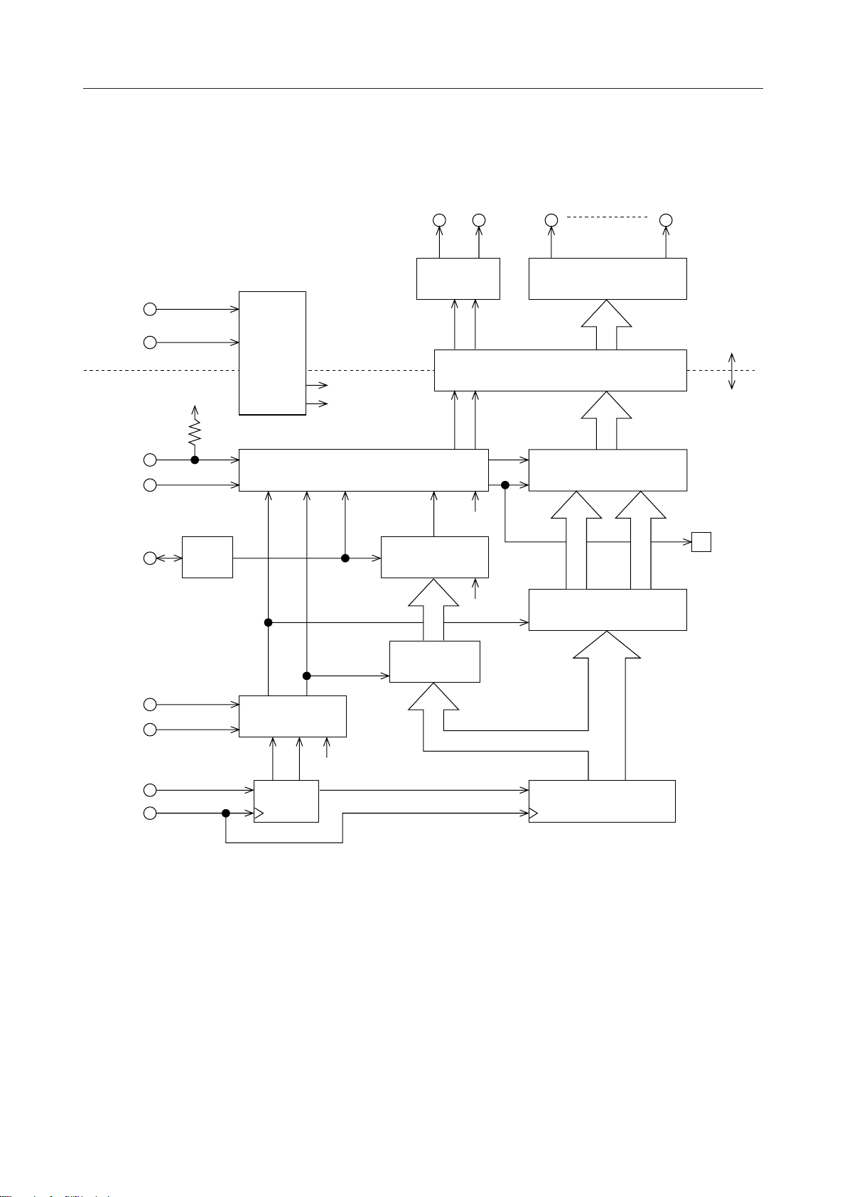
BLOCK DIAGRAM
SEG42SEG1GRID2GRID1
V
DD
V
BLANK
MODEA
OSC
MODEB
LOAD
SS
5V
OSC
Voltage
Regulator
LOAD
Timing Control
5V
POR
Timing Generator
Digital Dimming
L
2-bit
Grid Driver
10-bit
10-bit Latch
42-bit Segment Driver
Level Shifter
POR
POR
L
10-bits (Q1 to Q10)
Multiplexer
84-bit Latch
84 bits
VDD=8 to 18V
=5.0V
V
CC
(Regulator)
SEL
DATA
CLOCK
D
2-bit S/R
POR
D
Q1-Q84
84-bit Shift Register
2/15
Page 3
¡ Semiconductor MSC1209
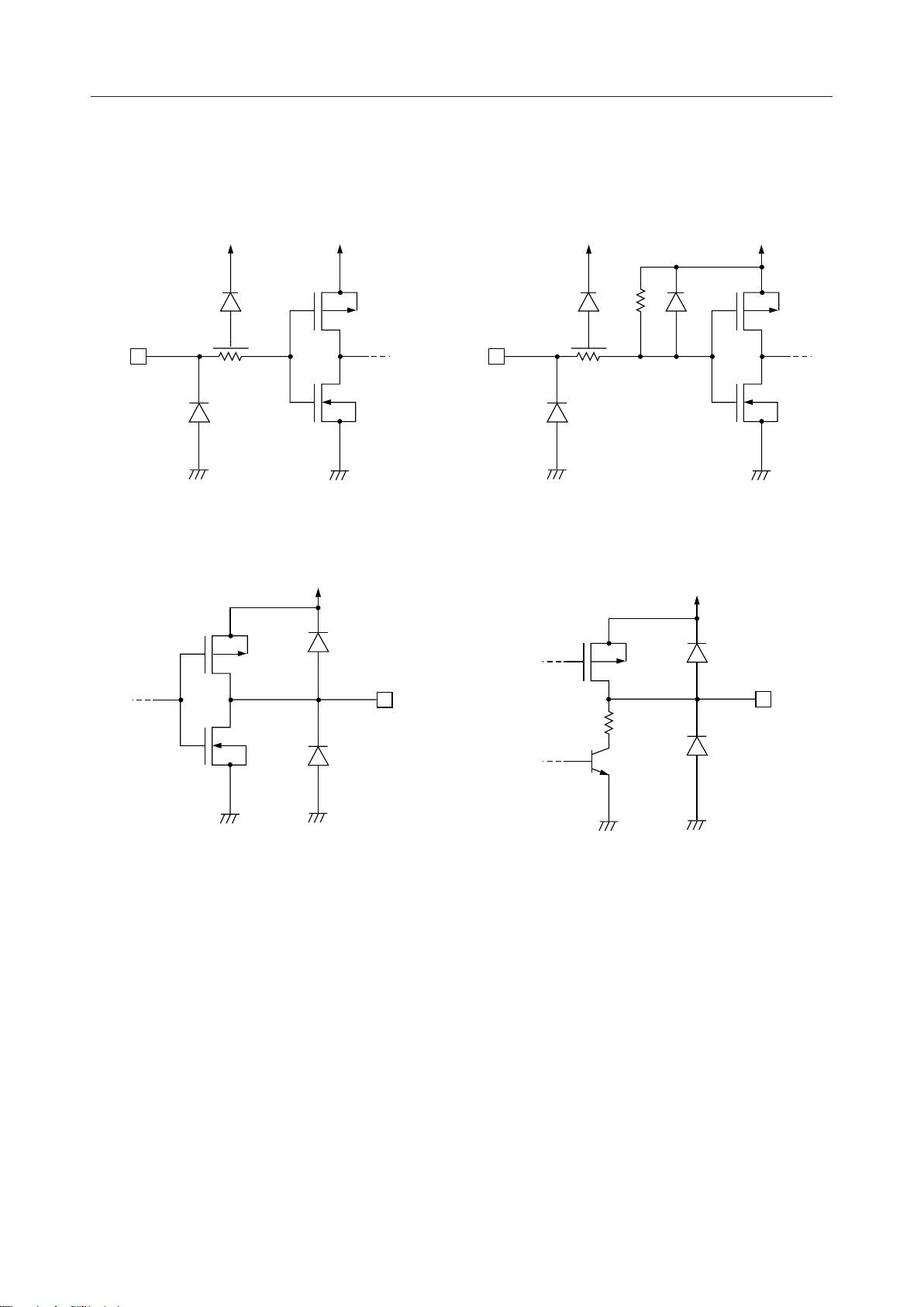
INPUT AND OUTPUT CONFIGURATION
• Schematic Diagram of Logic Portion Input
Circuit 1
INPUT
V
DD
V
SS
(5V Reg.)
V
SS
• Schematic Diagram of Logic Portion Output
Circuit
(5V Reg.)
• Schematic Diagram of Logic Portion Input
Circuit 2
SEL
V
DD
V
SS
(5V Reg.)
V
SS
• Schematic Diagram of Driver Output Circuit
V
DD
V
SS
OUTPUT
OUTPUT
V
SS
V
SS
V
SS
3/15
Page 4
¡ Semiconductor MSC1209
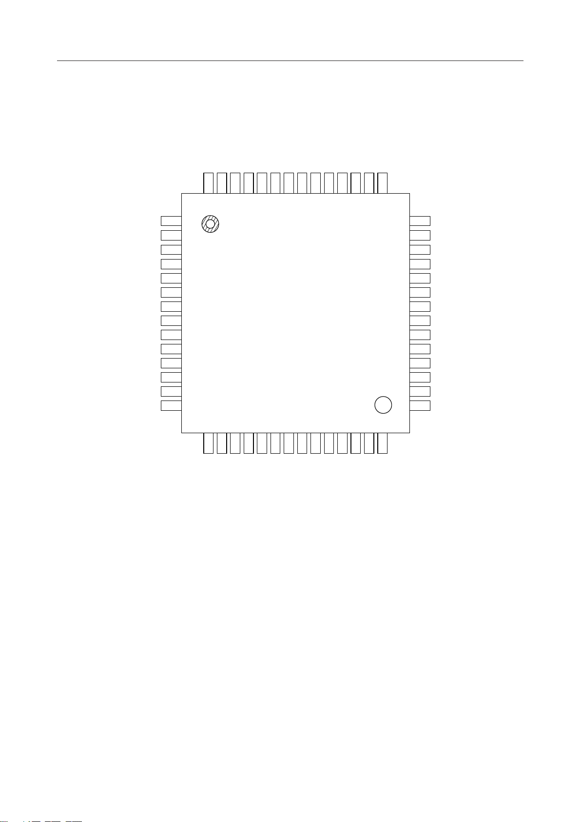
PIN CONFIGURATION (TOP VIEW)
SEG 4
SEG 5
SEG 6
SEG 7
SEG 8
SEG 9
SEG10
SEG11
SEG12
SEG13
SEG14
SEG15
SEG16
SEG17
10
11
12
13
14
SEG 1
SEG 2
SEG 3
56555453525150494847464544
1
2
3
4
5
6
7
8
9
15
SEL
MODEB
NC
DATA
CLOCK
LOAD
21222324252627
VSSMODEA
OSC
BLANK
GRID2
43
28
42
41
40
39
38
37
36
35
34
33
32
31
30
29
GRID1
V
DD
SEG42
SEG41
SEG40
SEG39
SEG38
SEG37
SEG36
SEG35
SEG34
SEG33
SEG32
SEG31
NC
SEG1816SEG1917SEG2018SEG2119SEG2220SEG23
NC: No connection
56-Pin Plastic QFP
SEG24
SEG25
SEG26
SEG27
SEG28
SEG29
SEG30
4/15
Page 5
¡ Semiconductor MSC1209
PIN DESCRIPTION
Pin Symbol
48 DATA
50
51 LOAD
1 to 20,
22 to 40,
54 to 56
42 GRID1
43 GRID2
44 BLANK
45 OSC
46 MODEA
52 MODEB
CLOCK
SEG1 to SEG42
Type
I
I
I
O
O
O
I
I/O
I
Connected to
Microcontroller
Microcontroller
Microcontroller
Anode electrode
of VFD tube
Grid electrode
of VFD tube
Grid electrode
of VFD tube
—
—
—
Description
Serial data input. (Positive logic)
Receives display data and dimming data.
Shift clock input.
Serial data is shifted on the rising edge of this shift clock
pulse.
Load pulse input.
The load signal is input when the transfer of serial data is
completed.
Segment driver output.
Grid driver output. When this pin is set to "L", the display
goes on. Connect an external PNP transistor to this pin.
The segment data of the first bit (S1) to the 42nd bit (S42) is
valid in the 84-bit segment data.
Grid driver output. When this pin is set to "L", the display
goes on. Connect an external PNP transistor to this pin.
The segment data of the 43rd bit (S43) to the 84th bit (S84)
is valid in the 84-bit segment data.
Input with pull-up resistor for display blank. When this pin is
set to "L", the display goes off. (SEGn="L")
Input and output for oscillation. Connect an external
capacitor of 68pF.
The typical value of oscillating frequency
is 512kHz.
These pins specify the operating mode.
MODEA MODEB
0 0 Master Operation
10
01
1 1 Slave Operation
Operating Mode
Test Mode
Slave Operation
45
68pF
53 SEL
41 V
47 V
DD
SS
O
—
—
MODEA pin
at slave side
Power source
Power source
SEL pin of the master IC outputs switching signals for the
segment data that corresponds to the grid signals. The SEL
pin of the master IC is connected to the MODEA pin of the
slave IC.
Power supply pin (8V to 18V).
GND pin. (Ground)
5/15
Page 6

¡ Semiconductor MSC1209
ABSOLUTE MAXIMUM RATINGS
Parameter
Power Supply Voltage
Input Voltage
Power Dissipation
Symbol
V
DD
V
IN
P
D
STG
Condition
—
All input pins
Ta≥25°C
—Storage Temperature T
RECOMMENDED OPERATING CONDITIONS
Parameter
Power Supply Voltage — — 18.0 V8.0
"H" Input Voltage
"L" Input Voltage All input pins other than OSC
"H" Driver Output VDD=10.8V, 1 driver at the ON state
Current VDD=10.8V, all drivers at the ON state
CLOCK Frequency — — 1.0 MHz—
Oscillation Frequency C=68pF
Grid Frequency C=68pF
Operating Temperature — — +105 °C–40
Symbol
V
DD
V
IH
V
IL
I
O–1
I
O–2
f
C
f
OSC
f
GRID
T
OP
Condition
All input pins other than OSC
–0.3 to +20
–0.3 to +6.0
–65 to +150
Min.
3.8
–0.3
—
—
307.2
150
Rating
257 mW
Typ.
—
—
—
—
512
250
Max.
5.5
+0.8
–2.2
–92.4mAmA
716.8
350
Unit
V
V
°C
Unit
V
V
kHz
Hz
6/15
Page 7

¡ Semiconductor MSC1209
ELECTRICAL CHARACTERISTICS
DC Characteristics
Unless otherwise specified: Ta=–40 to +105°C, VDD=8.0 to 18.0V
Parameter
"H" Input Voltage
"L" Input Voltage —
"H" Input Current I
"L" Input Current I
"H" Output Voltage VDD=9.5V, I
"L" Output Voltage VDD=9.5V, I
Supply Current
Symbol
V
IH
V
IL
IH1
I
IH2
IL1
I
IL2
V
OH1
V
OH2
V
OH3
V
OH4
V
OH5
V
OL1
V
OL2
V
OL3
V
OL4
V
OL5
V
OL6
I
DD
Condition
—
VDD=18.0V, V
VDD=18.0V, V
VDD=18.0V, V
VDD=18.0V, V
VDD=12.0V, I
VDD=15.0V, I
VDD=9.5V, I
VDD=12.0V, I
VDD=9.5V, I
VDD=9.5V, I
VDD=9.5V, I
VDD=9.5V, I
VDD=12.0V, I
f
=512kHz, no load — 20
OSC
Min.
3.8
–0.3
=5.0V –1.0
IH1
=5.0V –60 +60 mA
IH2
=0.0V –1.0 +1.0 mA All input pins
IL1
=0.0V –500 –100 mA
IL2
=–2.0mA
OH1
=–2.5mA
OH2
=–3.0mA
OH3
=–0.8mA
OH4
=–1.0mA 4.0 — V SEL
OH5
=500mA
OL1
=200mA
OL2
=1.0mA
OL3
=500mA
OL4
=200mA — 1.0 V
OL5
=1.0mA — 1.0 V SEL
OL6
VDD–0.5
VDD–0.5
V
–0.5
DD
–0.5
V
DD
—
—
—
—
Max.
5.5
+0.8
+1.0
—
—
—
—
4.0
2.0
4.0
2.0
Unit
V
V
mA
All input pins
other than BLANK
other than BLANK
V
V
V
V
V
V
V
V
mA
Applied pin
All input pins
BLANK
BLANK
SEG1 to 42
SEG1 to 42
GRID1 to 2
V
DD–VSS
AC Characteristics
Parameter Symbol Condition Min. Max. Unit
CLOCK Frequency f
CLOCK Pulse Width t
CLOCK Rise/Fall Time t
DATA Setup Time t
DATA Hold Time t
CLOCKÆ LOAD Time t
LOADÆ CLOCK Time t
LOAD Pulse Width t
SEGn Rise/Fall Time t
SEL Rise/Fall Time t
V
-DATA Input Time at VDD ON f
DD
V
-Hold Time at VDD OFF f
DD
VDD Rise Time at VDD ON f
C
(1/t
CR/tCF
(Ta=–40 to +85°C, V
) — — 1.0 MHz
CLOCK
CW
— 400 — ns
— — 300 ns
DS
DH
CL
LC
LW
R/tF
R/tF
PDA
PDF
PR2
When mounted in a unit 300 — ms
When mounted in a unit 5.0 — ms
— 200 — ns
— 200 — ns
— 100 — ns
— 100 — ns
— 1.0 — ms
CL=50pF — 1.0 ms
CL=50pF — 1.0 ms
— 100 ms—
=8 to 18V)
DD
7/15
Page 8

¡ Semiconductor MSC1209
TIMING DIAGRAM
1) Data Timing
SEL
t
CR
CLOCK
t
t
DH
DS
DATA
VALID VALID VALID VALID
2) Reset Timing
t
V
DD
PRZ
t
PDA
DATA
3) Output Timing
SEGn, GRIDn
t
CF
tRt
t
LW
3.8V
0.8V
t
CLOCK
t
CL
t
t
CW
t
CW
LC
3.8V
0.8V
3.8V
0.8V
80%V
t
POF
DD
0.0V
3.8V
0.8V
0.8V
0.2V
DD
DD
SEL
F
t
RtF
4.0V
1.0V
8/15
Page 9

¡ Semiconductor MSC1209
FUNCTIONAL DESCRIPTION
DATA Input
This device uses 10-bit dimming data (D1 to D10) and 84-bit segment data (S1 to S84). To transfer
these data, the mode bits (M0 and M1) must be sent after each of these data succeedingly. The
data transfer timing diagram is shown below.
D10
DATA
CLOCK
LOAD
D2D1
M0 S1 S2
Figure 1 Data Transfer Timing
S83M1S84
M0 M1
M0 : Enable bit
M0 = "0": Indicates the data from the master IC.
M0 = "1": Indicates the data from the slave IC.
M1 : Mode specification bit
M1 = "1": Indicates that the data sent on ahead is dimming data.
M1 = "0": Indicates that the data sent on ahead is segment data.
D1 : LSB of dimming data
S1 : data for GRID1 of SEG1
S2 : data for GRID1 of SEG2
:
S42 : data for GRID1 of SEG42
S43 : data for GRID2 of SEG1
:
S84 : data for GRID2 of SEG42
Notes: 1. When the number of input data bits are larger, the data bits are pushed out in the
same order that they are input, and 86 bits of the data counted from the bit entered
last are used as valid data. (In the case of segment data)
2. When the number of input data bits are smaller, the data remaining in the shift
register before data transfer is shifted and used as valid data.
CLOCK Input
Data is shifted at the rising edge of the clock.
LOAD Input
The contents of the shift register are shifted in while the LOAD input is "H" level and latched at
"H" to "L" transition. This LOAD signal is regenerated in the VFD tube driver for the latch pulse
for dimming data and segment data. When 10-bit dimming data and 84-bit segment data have
been transferred, input the LOAD signal prior to the next clock.
9/15
Page 10

¡ Semiconductor MSC1209
Blank Function
Inputting a "L" level to the BLANK pin turns display off (segment output = "L"). At this
time, grid outputs are output normally.
Initial Setting
When power is turned on (i.e., when segment data has never been transferred), the display is
turned off (segment output = "L"). Display is turned on at the moment when transfer of the
segment data is complete. The relationship between the data transfer and display is shown in
Figure 2.
V
DD
DATA
LOAD
SEGn
Dimming Data
Display OFF
Segment Data
Display ON
Figure 2 Relationship Between Data Transfer and Display
If, after power-on, the segment data is transferred before the dimming data is transferred, display
is turned on at the moment when transfer of the segment data is complete, at which time the
dimming value is undefined. The relationship between the data transfer and display is shown
in Figure 3.
V
DD
DATA
Segment Data
Dimming Data
LOAD
SEGn
Display OFF Display ON
Undefined Dimming Value
Figure 3 Relationship Between Advanced Transfer of Segment Data and Display
10/15
Page 11

¡ Semiconductor MSC1209
Oscillator
Connect an external capacitor (C), as shown in Figure 4. The oscillating frequency f
on the external capacitor used. The following equation is true between f
(f
GRID
f
GRID
):
= f
OSC
/2048
C (68pF)
OSC Pin
f
OSC
and grid frequency
OSC
OSC
depends
Figure 4 Oscillator Equivalent Circuit
Dimming Function
The duty cycle of grid output can be changed in 1/2048 step with respect to 10-bit dimming data.
Table 1 shows the relationship between dimming data and duty ratio.
Table 1 Dimming Data and Duty Ratio
(MSB)
00
00
~
11
11
11
~
11
Dimming Data
0000
0000
~~
1111
1111
1111
1111
(LSB)
0000
0001
~~
0111
1000
1001
1110
Duty Ratio
0/2048
1/2048
~~
1015/2048
1016/2048
1016.5/2048
1016.5/2048
Max
Ø
Max
Note: Setting for address 3FFH is invalid.
Duty ratios are programmable within the range of 0/2048 (0%) to 1016.5/2048 (49.6%). Figure
5 shows the grid output timing.
Cascade Connection
When two MSC1209 ICs are used in cascade connection, use the MODEA and MODEB pins to
connect them, as shown below.
MSC1209
MODEA
MODEB
OSC
(Master)
SEL
5V
MSC1209
MODEA
MODEB
OSC
(Slave)
SEL
OPEN
11/15
Page 12

¡ Semiconductor MSC1209
The IC where the MODEA and MODEB pins are set to "L" operates as the master, and the one
where the MODEB pin is set to "H" as the slave.
By connecting the master side SEL output pin to the slave side MODEA pin, the segments on the
slave side operate in synchronization with the grid on the master side.
12/15
Page 13

¡ Semiconductor MSC1209
GRID Output Timing
t
FOSC
)
(f
OSC
SEGn
S43 - S84
t
BLANK1
t
SEL
* Dimming Data; 3FE[H] to 3F9[H]
GRID1
GRID2
Display ON
Display OFF
* Dimming Data; 3F8[H]
GRID1
GRID2
Display ON
Display OFF
BLANK2
t
GRID
S1 - S42 S43 - S84
Display ON
Display OFF
Display ON
Display OFF
Display OFF
Display ON
Display OFF
Display ON
* Dimming Data; 002[H]
GRID1
GRID2
* Dimming Data; 001[H]
GRID1
GRID2
* Dimming Data; 000[H]
GRID1
GRID2
t
= 2ms Typical
FOSC
t
= 2048t
GRID
t
BLANK1
= 2t
FOSC
FOSC
Display OFF
ON
Display OFF
Display OFF
ON ON
Display OFF
ON
ON
Display OFF
Display OFF
Display OFF
Display OFF
, t
BLANK2
= 5.5t
FOSC
ON
Figure 5 Dimming Data and Duty Ratio
13/15
Page 14

¡ Semiconductor MSC1209
APPLICATION CIRCUIT
* When one MSC1209 IC is used
(SEG1 to 42) ¥ 1
SEG42
GRID1
GRID2
CPU
SEG1
LOAD
CLOCK
DATA
SEL
MODEA
MODEB
OSC
V
SS
V
DD
* When two MSC1209 ICs are used
SEG1
SEG42
VF Display Tube
(SEG1 to 42) ¥ 2
SEG1 SEG42
CPU
LOAD
CLOCK
DATA
MODEA
MODEB
OSC
V
SS
GRID1
GRID2
SEL
V
DD
5V
LOAD
CLOCK
DATA
MODEA
MODEB
OSC
V
SS
GRID1
GRID2
V
DD
VF Display Tube
14/15
Page 15

¡ Semiconductor MSC1209
PACKAGE DIMENSIONS
(Unit : mm)
QFP56-P-910-0.65-2K
Mirror finish
Package material
Lead frame material
Pin treatment
Solder plate thickness
Package weight (g)
Epoxy resin
42 alloy
Solder plating
5 mm or more
0.43 TYP.
Notes for Mounting the Surface Mount Type Package
The SOP, QFP, TSOP, TQFP, LQFP, SOJ, QFJ (PLCC), SHP, and BGA are surface mount type
packages, which are very susceptible to heat in reflow mounting and humidity absorbed in
storage. Therefore, before you perform reflow mounting, contact Oki’s responsible sales person
on the product name, package name, pin number, package code and desired mounting conditions
(reflow method, temperature and times).
15/15
Page 16

E2Y0002-29-11
NOTICE
1. The information contained herein can change without notice owing to product and/or
technical improvements. Before using the product, please make sure that the information
being referred to is up-to-date.
2. The outline of action and examples for application circuits described herein have been
chosen as an explanation for the standard action and performance of the product. When
planning to use the product, please ensure that the external conditions are reflected in the
actual circuit, assembly, and program designs.
3. When designing your product, please use our product below the specified maximum
ratings and within the specified operating ranges including, but not limited to, operating
voltage, power dissipation, and operating temperature.
4. Oki assumes no responsibility or liability whatsoever for any failure or unusual or
unexpected operation resulting from misuse, neglect, improper installation, repair, alteration
or accident, improper handling, or unusual physical or electrical stress including, but not
limited to, exposure to parameters beyond the specified maximum ratings or operation
outside the specified operating range.
5. Neither indemnity against nor license of a third party’s industrial and intellectual property
right, etc. is granted by us in connection with the use of the product and/or the information
and drawings contained herein. No responsibility is assumed by us for any infringement
of a third party’s right which may result from the use thereof.
6. The products listed in this document are intended for use in general electronics equipment
for commercial applications (e.g., office automation, communication equipment,
measurement equipment, consumer electronics, etc.). These products are not authorized
for use in any system or application that requires special or enhanced quality and reliability
characteristics nor in any system or application where the failure of such system or
application may result in the loss or damage of property, or death or injury to humans.
Such applications include, but are not limited to, traffic and automotive equipment, safety
devices, aerospace equipment, nuclear power control, medical equipment, and life-support
systems.
7. Certain products in this document may need government approval before they can be
exported to particular countries. The purchaser assumes the responsibility of determining
the legality of export of these products and will take appropriate and necessary steps at their
own expense for these.
8. No part of the contents cotained herein may be reprinted or reproduced without our prior
permission.
9. MS-DOS is a registered trademark of Microsoft Corporation.
Copyright 1999 Oki Electric Industry Co., Ltd.
Printed in Japan
 Loading...