

Page 1

E2C0018-27-Y3
¡ Semiconductor MSC1205
¡ Semiconductor
This version: Nov. 1997
Previous version: Jul. 1996
MSC1205
32-Bit Duplex Controller/Driver with Digital Dimming Function
GENERAL DESCRIPTION
The MSC1205 is a Bi-CMOS display driver for a 1/2-duty vacuum fluorescent display tube. It
consists of a 64-bit shift register, latch circuits, a digital diming circuit, and drivers.
The MSC1205 provides an interface with a microcomputer only by three signal lines: LOAD,
DATA, and CLOCK.
FEATURES
• Power Supply Voltage: 8 to 18V (built-in 5V regulator for logic)
• Built-in 1-terminal RC oscillation circuit (with external capacitor)
• Built-in digital dimming circuit
10-bit resolution
Programmable in the duty range of 0/2048 (0%) to 1015.5/2048 (49.6%).
• Can directly drive 32 ¥ 2 display anodes.
• Built-in power-on reset circuit
• Package options:
42-pin plastic DIP (DIP42-P-600-2.54) (Product name: MSC1205-RS)
44-pin plastic QFP (QFP44-P-910-0.80-2K) (Product name: MSC1205GS-2K)
1/15
Page 2
¡ Semiconductor MSC1205
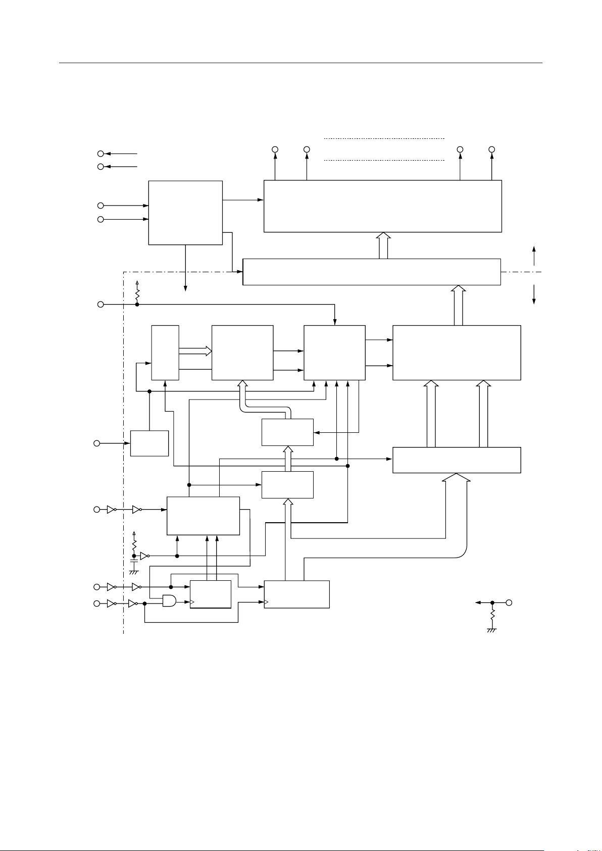
BLOCK DIAGRAM
GRID1
GRID2
V
DD
V
SS
BLANK
OSC
LOAD
VOLTAGE
REGULATOR
5V
DOWN COUNTER
10 bits
bo
R
(fosc)
OSC
LOAD TIMING
CONTROL
(POR)
COMPA-
RATOR
10 bits
(SEGLD)
(DIMLD)
SEG32
L
SEG31 SEG2 SEG1
DRIVER
32 bits
LEVEL SHIFTER
BL
MULTIPLEXER
ST
32 bits 32 bits
(bo)
LATCH
TIMING
GENE-
RATOR
L
L
LATCH
LATCH
Q1-Q10
Q1-Q64
32 bits
64 bits
8 to 18V
5V
DATA
CLOCK
D
(2 bits)
D
Q1-Q64
(64 bits)
SHIFT REGISTER
TEST
2/15
Page 3
¡ Semiconductor MSC1205
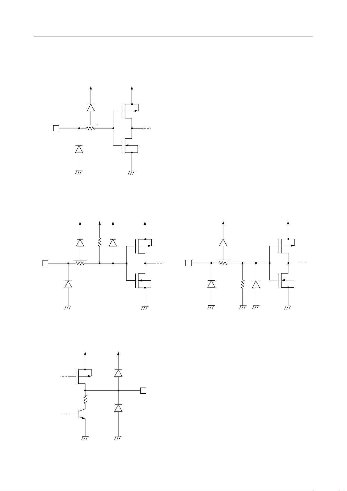
INPUT AND OUTPUT CONFIGURATION
• Schematic Diagrams of Logic Portion Input Circuit 1
V
DD
(5V Reg.)
INPUT
V
SS
V
SS
• Schematic Diagrams of Logic Portion Input
Circuit 2
BLANK
V
DD
(5V Reg.)
• Schematic Diagrams of Logic Portion Input
Circuit 3
TEST
V
DD
(5V Reg.)
V
SS
V
SS
• Schematic Diagrams of Driver Output Circuit
V
DD
V
SS
V
DD
V
OUTPUT
SS
V
SS
V
SS
3/15
Page 4
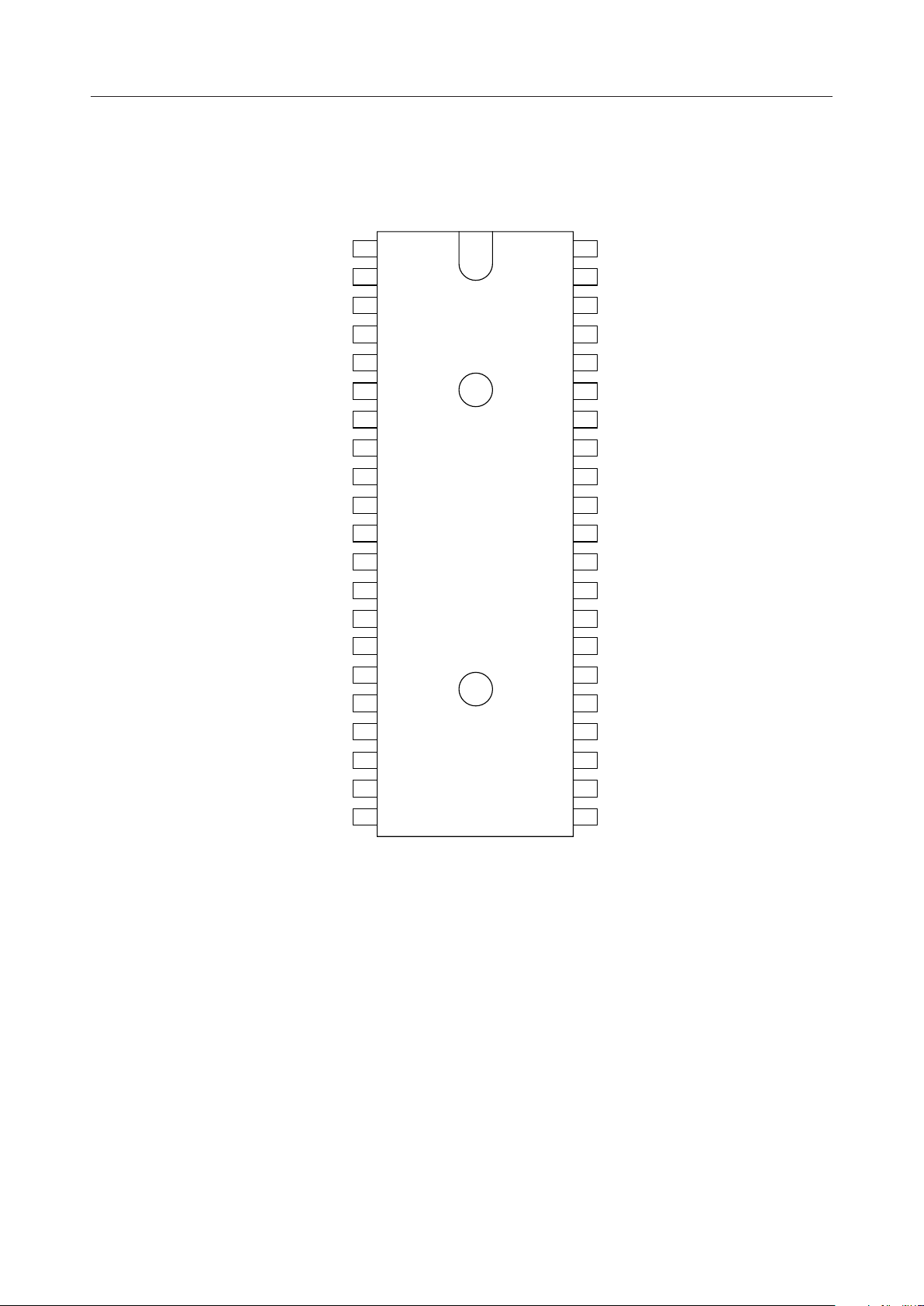
¡ Semiconductor MSC1205
PIN CONFIGURATION (TOP VIEW)
DATA V
CLOCK TEST
LOAD OSC
SEG1
SEG2 GRID2
SEG3 GRID1
SEG4 V
SEG5 SEG32
SEG6 SEG31
SEG7 SEG30
SEG8 SEG29
SEG9 SEG28
SEG10 SEG27
SEG11 SEG26
SEG12 SEG25
SEG13 SEG24
1
42
SS
241
3
4
40
39
BLANK
538
637
7
36
DD
835
9
10
11
12
34
33
32
31
13 30
14
29
15 28
16 27
SEG14 SEG23
SEG15 SEG22
SEG16 SEG21
SEG17 SEG20
SEG18 SEG19
17 26
18
25
19 24
20 23
21 22
42-Pin Plastic DIP
4/15
Page 5
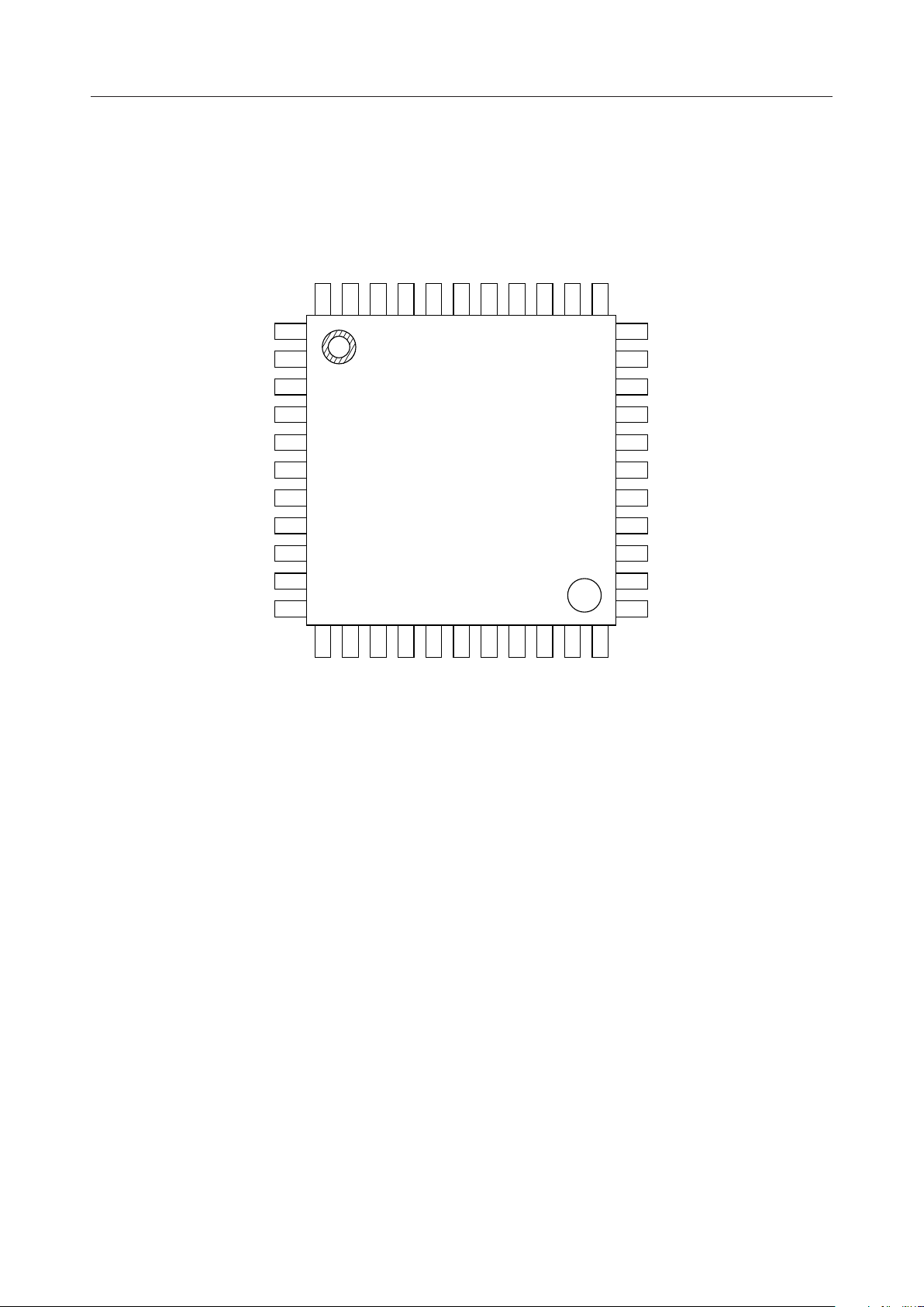
¡ Semiconductor MSC1205
PIN CONFIGURATION (TOP VIEW)
SS
TEST
OSC
BLANK
35
GRID2
34
SEG2
44
SEG1
43
LOAD
42
CLOCK
DATANCV
41
40
39
38
37
36
SEG3
SEG4
SEG5
SEG6
SEG7
SEG8
SEG9
SEG10
SEG11
SEG12
SEG13
10
11
1
2
3
4
5
6
7
8
9
12
13
14
15
16
17
18
19
20
21
SEG14
SEG15
SEG16
SEG17
SEG18NCSEG19
SEG20
SEG21
SEG22
33
32
31
30
29
28
27
26
25
24
23
22
SEG23
GRID1
V
DD
SEG32
SEG31
SEG30
SEG29
SEG28
SEG27
SEG26
SEG25
SEG24
NC : No-connection pin
44-Pin Plastic QFP
5/15
Page 6

¡ Semiconductor MSC1205
PIN DESCRIPTION
Symbol
DATA
CLOCK
LOAD
SEG1
-SEG32
V
DD
GRID1
GRID2
BLANK
OSC
TEST
Type
I
I
I
O
—
O
O
I
I
I
Description
Serial data input pin. This pin receives display data, dimming data, enable bit and mode bit.
Shift clock input pin with Schmitt circuit.
Serial data is clocked in this pin at the rising edge of the shift clock pulse.
Load pulse input pin.
The load signal is input when dimming data and segment data transfer is finished.
Segment driver output pins. These pins provide large current
driving (I
driving (I
= –5.5mA at VDD = 12V) and small current
OH
= –1.8mA at VDD = 12V).
OH
Power supply voltage. This pin is connected to a power supply of 8 to 18V.
Grid driver output pin. When this pin is set to "L", the display is turned on. This pin is connected
to external PNP transistor.
The segment data of the first bit (S1) to the 32nd bit (S32) is valid in the segment data of 64
bits.
Grid driver output pin. When this pin is set to "L", the display is turned on. This pin is connected
to external PNP transistor.
The segment data of the 33rd bit (S33) to the 64th bit (S64) is valid in the segment data of 64
bits.
Display blank input pin with a pull-up resistor.
When this pin is set to "L", the display is turned off (SEGn = "L")
Oscillation input pin. This pin is connected to an external capacitor of 82pF. A standard
oscillation frequency is 512kHz.
Test input pin with a pull-down resistor.
Normally this pin should be left open or should be connected to ground.
V
SS
Ground pin.
—
This pin is connected to ground (V
SS
= 0)
6/15
Page 7

¡ Semiconductor MSC1205
ABSOLUTE MAXIMUM RATINGS
Parameter Symbol Condition Rating Unit
Supply Voltage V
DD
IN
STG
Ta = 25°C
Ta = 25°CInput Voltage V
—Storage Temperature Range T
–0.3 to +20 V
–0.3 to +6.0 V
–65 to +150 °C
RECOMMENDED OPERATING CONDITIONS
Parameter Symbol Condition Range Unit
Power Supply Voltage V
DD
op
—
—Operating Temperature Range T
8 to 18 V
–40 to +85 °C
ELECTRICAL CHARACTERISTICS
DC Characteristics
(Ta = –40 to +85˚C, V
Parameter Symbol Condition Min. Max. Applicable pin
High Level Input Voltage
Low Level Input Voltage
High Level Input Current
V
V
I
IH1
IH
IL
—
—
VI = 5V
3.8
–0.3 0.8
–1
5.5
1 DATA, LOAD
Unit
V
V
mA
= 8 to 18V)
DD
CLOCK
—
—
Low Level Input Current
High Level Output
Voltage (1)
(Small Current Driver)
High Level Output
Voltage (2)
(Large Current Driver)
Low Level Output
Voltage
High Level Output
Voltage (3)
Current Consumption
V
V
V
V
V
V
V
V
I
IH3
I
IL1
I
IL2
I
IL3
OH1
OH2
OH3
OH4
OH5
OH6
OL1
OL2
OL3
OH7
I
DD
VI = 5V
V
V
V
= 9.5V, I
V
DD
= 12V, I
V
DD
VDD = 15V, I
= 9.5V, I
V
DD
VDD = 12V, I
= 15V, I
V
DD
= 9.5V, I
V
DD
V
= 9.5V, I
DD
= 9.5V, I
V
DD
VDD = 9.5V, I
f
= 512kHz, no load
OSC
= 0V
I
= 0V
I
= 0V
I
OH1
OH2
OH3
OH4
OH5
OH6
OL2
OH7
= –1.3mA
= –1.8mA
= –2.3mA
= –4.1mA
= –5.5mA
= –7.0mA
= 1mA
OL1
= 500mA
= 2mA
OL3
= –0.8mA
–500
V
DD
V
DD
V
DD
V
DD
V
DD
V
DD
V
DD
—
–1
–1
—
—
-0.5
-0.5
-0.5
-0.5
-0.5
-0.5
-0.5
500
1
–100
1
—
—
—
—
—
—
4
2
0.3
—
20
mA
mA
mA
mA
V
V
V
V
V
V
V
V—V
V—V
V
mA
TEST
DATA, LOAD
CLOCK
BLANK
TEST
SEG (2n)
n = 1-16
SEG (2n-1)
n = 1-16
SEG1-SEG32
GRID1, GRID2
GRID1, GRID2
—
7/15
Page 8

¡ Semiconductor MSC1205
AC Characteristics
Parameter Symbol Condition Min. Typ. Max. Unit
Clock Frequency f
Clock Pulse Width
Clock Rise/Fall Time
DATA Setup Time
DATA Hold Time
Clock Æ Load Time
Load Æ Clock Time
Load Pulse Width
Large Current
SEGn Rise/Fall Time
Small Current
Grid Frequency
Oscillation Frequency
(1/tclock)
C
t
CW
tcr, t
cf
t
DS
t
DH
t
CL
t
LC
t
LW
tr, t
f
tr, t
f
f
GRID
f
OSC
—
—
—
—
—
—
—
—
C
= 20pF
L
C
= 20pF
L
= 82pF±5%
C
L
(Ta = –40 to +85˚C, V
—
500
—
200
200
100
50
1.3
0
0
150
307.2
—1
—
—
—
—
—
—
—
4/120
15/120
250
512
= 8 to 18V)
DD
—
500
—
—
—
—
—
400
400
350
716.8
MHz
ns
ns
ns
ns
ns
ns
ms
ns
ns
Hz
kHz
DATA
CLOCK
LOAD
DATA
CLOCK
LOAD
SEGn
GRIDn
SEGMENT DATA DIMMING DATA
3.8V
0.8V
t
DS
t
DH
f
C
t
CW
t
CW
3.8V
t
CL
t
t
cr
cf
t
LC
3.8V
0.8V
0.8V
t
t
r
t
f
0.9V
DD
0.1V
DD
LW
8/15
Page 9

¡ Semiconductor MSC1205
FUNCTIONAL DESCRIPTION
DATA Input
This device uses 10-bit dimming and 64-bit segment data.
In order to transfer this data, the enable bit (M0) and mode bit (M1) should be set to an initial state.
The data format is shown below.
DATA
CLOCK
M1M0 D1 D2 D10 M0 M1 S1 S2 S63 S64
Figure 1. Data Transfer Timing
M0 : This bit is an enable bit.
M0 = "0" : Subsequent data is disabled; preceding data is held.
M0 = "1" : The beginning of data transfer. The following data is clocked in sequentially.
M1 : This bit is used to select the mode.
M1 = "0" : Subsequent data is handled as the segment data.
M1 = "1" : Subsequent data is handled as the dimming data.
D1 : LSB of dimming data.
S1 : data for grid1 of SEG1.
S2 : data for grid1 of SEG2.
.
.
.
S32 : data for grid1 of SEG32.
S33 : data for grid2 of SEG1.
.
.
.
S64 : data for grid2 of SEG32.
Notes: 1. Be sure to set the enable bit to "1" before data is transferred. Data following M0 is
handled to be enable. If data is input with the enable bit not set to "1", the first "1"
data coming next is handled as the enable bit.
2. If the number of the data bits applied is greater (for example, 67 bits are applied
for the segment data of 64 bits), the data bits are pushed out in the same order
that they are applied, and thus S1, S2, and S3 are ignored.
3. If the number of the data bits applied is smaller (for example, 62 bits are applied
for the segment data of 64 bits), S63 and S64 prior to data transfer are shifted to S1
and S2 respectively.
9/15
Page 10

¡ Semiconductor MSC1205
CLOCK Input
DATA is shifted at the rising edge of the clock.
LOAD Input
The contents of the shift register are shifted in while the LOAD input is "H" and latched at "H"
to "L" transition.
The LOAD signal is reproduced in the VF driver for the latch pulse for dimming data and
segment data.
After 10-bit dimming data and 64-bit segment data are transferred, input the LOAD signal prior
to the next clock.
Blank Function
A low-level voltage at the BLANK pin turns the display off (segment output = "L"). When
segment data transfer is finished, the display is turned on.
The relationship between this data transfer and the display is shown in Figure 2.
Initial Setting
When powered on (i.e., when the segment data has never been transferred) the display is turned
off (the segment output is "L").
When segment data transfer is finished, display is turned on. The relationship between this data
transfer and the display is shown in Figure 2.
V
DD
DATA
LOAD
SEGn
Display OFF Display ON
SEGMENT DATADIMMING DATA
Figure 2. Relationship Between Data Transfer and Display
10/15
Page 11

¡ Semiconductor MSC1205
If the segment data is transferred before the dimming data is transferred after powered on, the
display is turned on at the completion of segment data transfer, with undefined dimming values.
The relationship between data transfer and display is shown in Figure. 3.
V
DD
DATA
LOAD
SEGn
SEGMENT DATA DIMMING DATA
Dimming value is undefined
Display OFF Display ON
Figure 3. Relationship Between Advance Transfer of Segment Data and Display
Oscillator
Connect an external capacitor (C), as shown in Figure 4. The oscillating frequency f
on the external capacitor used. The following equation is true between f
(f
GRID
):
f
GRID
= f
OSC
/2048
Terminal
f
OSC
and grid frequency
OSC
depends
OSC
C (82pF)
Figure 4. Oscillation Equivalent Circuit
11/15
Page 12

¡ Semiconductor MSC1205
Dimming Function
The duty cycle of grid output can be changed in 1/2048 step with respect to 10-bit dimming data.
Table 1 shows the relationship between dimming data and duty ratio.
Table 1. Dimming Data and Duty Ratio
(MSB) dimming data (LSB)
00
00
~
11
11
~
11
0000
0000
~
1111
1111
~
1111
0000
0001
~
0111
1000
~
1110
Duty ratio
0/2048
1/2048
~
1015/2048
1015.5/2048
~
1015.5/2048
Max
Æ
Max
Note: Setting for address 3FFH is invalid.
Duty ratios are programmable within the range of 0/2048 (0%) to 1015.5/2048 (49.6%).
12/15
Page 13

¡ Semiconductor MSC1205
APPLICATION CIRCUIT
SEG1-SEG32
45 35
SEG1 SEG32
SEG2
1
DATA
2
CPU
3
CLOCK
LOAD
GRID1
GRID2
37
38
40
82pF
OSC
MSC1205
V
SS
V
DD
42 36
VFD
13/15
Page 14

¡ Semiconductor MSC1205
PACKAGE DIMENSIONS
(Unit : mm)
DIP42-P-600-2.54
Package material
Lead frame material
Pin treatment
Solder plate thickness
Package weight (g)
Epoxy resin
42 alloy
Solder plating
5 mm or more
6.20 TYP.
Notes for Mounting the Surface Mount Type Package
The SOP, QFP, TSOP, SOJ, QFJ (PLCC), SHP and BGA are surface mount type packages, which
are very susceptible to heat in reflow mounting and humidity absorbed in storage.
Therefore, before you perform reflow mounting, contact Oki’s responsible sales person for the
product name, package name, pin number, package code and desired mounting conditions
(reflow method, temperature and times).
14/15
Page 15

¡ Semiconductor MSC1205
(Unit : mm)
QFP44-P-910-0.80-2K
Mirror finish
Package material
Lead frame material
Pin treatment
Solder plate thickness
Package weight (g)
Epoxy resin
42 alloy
Solder plating
5 mm or more
0.41 TYP.
Notes for Mounting the Surface Mount Type Package
The SOP, QFP, TSOP, SOJ, QFJ (PLCC), SHP and BGA are surface mount type packages, which
are very susceptible to heat in reflow mounting and humidity absorbed in storage.
Therefore, before you perform reflow mounting, contact Oki’s responsible sales person for the
product name, package name, pin number, package code and desired mounting conditions
(reflow method, temperature and times).
15/15
 Loading...