

Page 1

E2C0017-27-Y2
¡ Semiconductor MSC1201-xx
¡ Semiconductor
This version: Nov. 1997
Previous version: Jul. 1996
MSC1201-xx
60-Bit VFD Tube Driver with Digital Dimming and PWM Conversion Function
GENERAL DESCRIPTION
The MSC1201-xx is a 1/2 duty vacuum fluorescent display tube driver implemented in Bi-CMOS
technology. This LSI consists of 64-bit shift registers, 64 latches, PWM conversion circuit, a digital
dimming circuit, 30-segment driver and 2-grid driver. As the MSC1201-xx has both a digital
dimming circuit and a PWM conversion circuit which converts PWM signal for lamp dimming
control to PWM signal for VFD tube dimming control, the dimming control can be realized
without any external circuit.
The interface with a MCU can be done only with 3 wires (CS, DATA and CLOCK signals). Also,
DATA and CLOCK signal lines can be shared with other peripherals because of chip select
function by CS signal.
For the general purpose code, the code number is -01. (Product name: MSC1201-01GS-2K)
For a custom code, the code number will be ordered at any time.
FEATURES
• Single supply voltage : VDD = 8 V to 18 V (built-in 5 V logic regurator)
• Operating temperature range : Ta = –40°C to +85°C
• 30-segment driver outputs (IOH = –6 mA at VOH = V
• 2-grid pre-driver outputs (IOH = –30 mA at VOH = V
• Built-in digital dimming circuit (11-bit resolution)
• Built-in oscillation circuit (external R and C, f
• Built-in Power-On-Reset circuit.
• Lamp PWM signal Æ Buil-in PWM conversion circuit for vacuum fluorescent display tube.
• Built-in RC Oscillation (external R and C)
• Correspondence between shift register and output segment is settable optionally using built
in mask programmable 30 ¥ 30 PLA.
• Package :
44-pin plastic QFP (QFP44–P–910-0.80–2K)(Product name: MSC1201-xxGS-2K)
= 2.0 MHz)
OSC
xx indicates the code number
DD
DD
– 0.8 V)
– 0.8 V)
1/20
Page 2
¡ Semiconductor MSC1201-xx
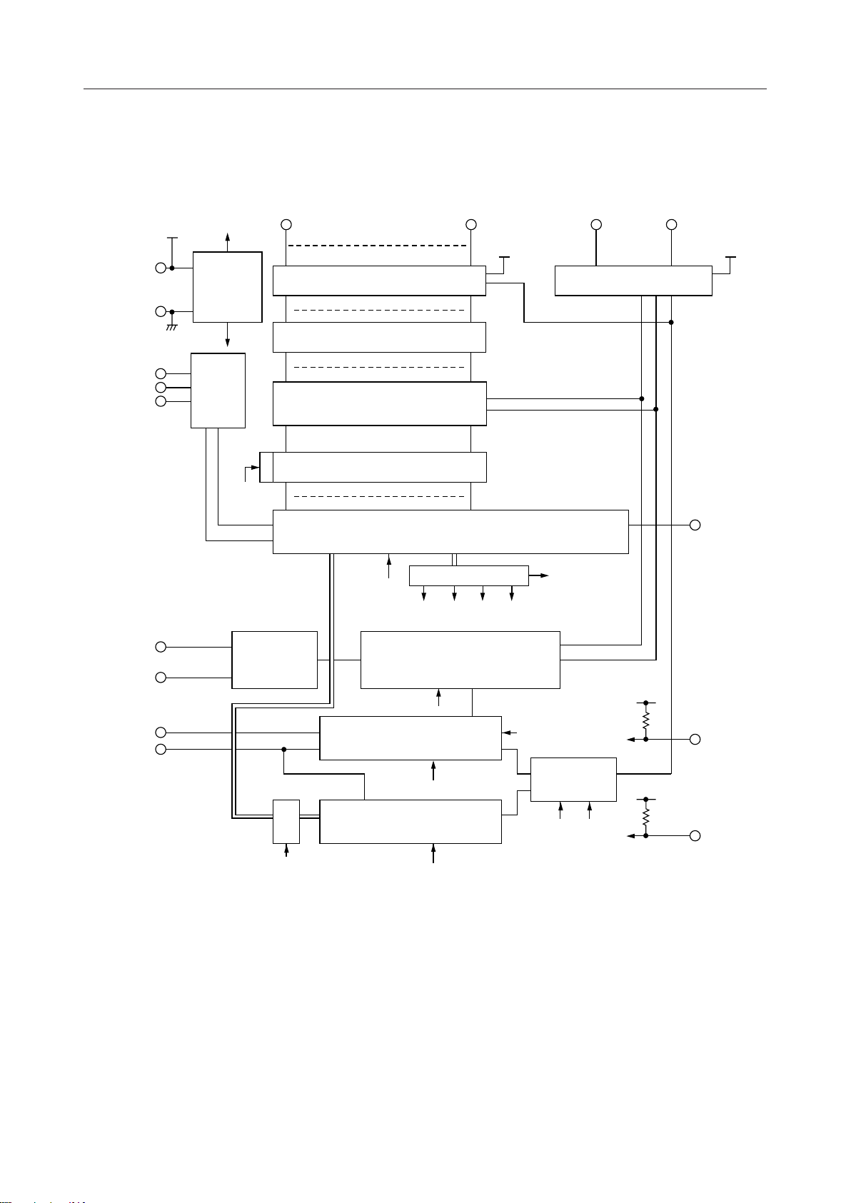
BLOCK DIAGRAM
V
DD
GND
CS
DATA
CLOCK
5 V
5 V Reg
&
POR Circuit
POR
Control
Circuit
S1
SEG1
D
CK
30-Segment Driver
30 ¥ 30 PLA Matrix
Multiplexer
Latch
64-Bit Shift Register
D48-59
R
POR
SEG30 GRID1 GRID2
2-Grid Driver
M3 M2 M1 M0
Mode Selector
S1 S2 S3 S4
Test Mode
DATA OUT
OSC0
OSC1
PWMIN
VK
RC
OSC
S2
Timing Generator
R
POR
PWM Conversion Circuit
R
POR
Digital Dimming Circuit
R
POR
S2
Selector
S3 S4
INH
TEST1
2/20
Page 3
¡ Semiconductor MSC1201-xx
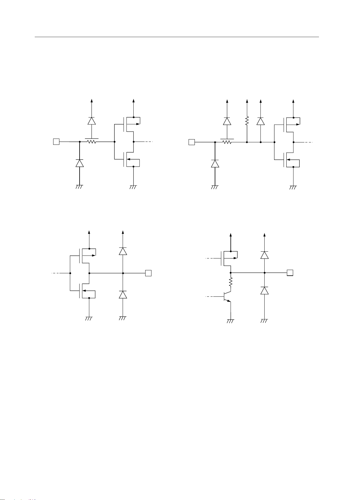
INPUT AND OUTPUT CONFIGURATION
• Schematic Diagrams of Logic Portion Input
Circuit 1
INPUT
V
DD
GND
(5V Reg.)
GND
• Schematic Diagrams of Logic Portion Output
Circuit
(5V Reg.)
(5V Reg.)
• Schematic Diagrams of Logic Portion Input
Circuit 1
TEST1
INH
V
DD
GND
(5V Reg.)
GND
• Schematic Diagrams of Driver Output Circuit
V
DD
V
DD
GND
GND
OUTPUT
GND
OUTPUT
GND
3/20
Page 4
¡ Semiconductor MSC1201-xx
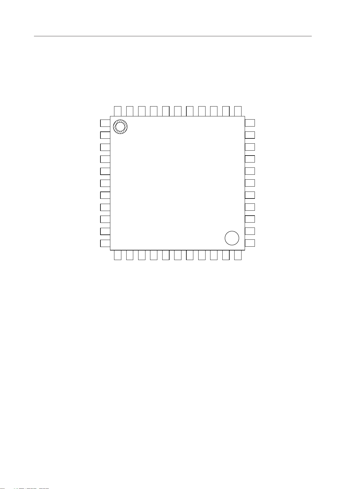
PIN CONFIGURATION (TOP VIEW)
SEG11
SEG12
SEG13
SEG14
SEG15
SEG16
SEG17
SEG18
SEG19
SEG20
SEG21
34
35
36
37
38
39
40
41
42
43
44
SEG10
SEG22
SEG23
1
2
33
32
SEG9
SEG24
SEG25
SEG26
SEG27
SEG28
SEG29
SEG30
GRID1
GRID2
10
11
3
4
5
6
7
8
9
21
20
19
18
17
16
15
14
13
12
V
DD
VK
OSC0
TEST1
OSC1
44-Pin Plastic Package
GND
CS
DATA
CLOCK
INH
31
30
29
28
27
26
25
24
23
22
PWM IN
SEG8
SEG7
SEG6
SEG5
SEG4
SEG3
SEG2
SEG1
DATAOUT
4/20
Page 5
¡ Semiconductor MSC1201-xx
PIN DESCRIPTIONS
Pin Symbol
1-9
24-44
10, 11
16
15
18
20
19
23
22
14
SEG1-30
OSC0
OSC1
CS
DATA
CLOCK
DATA
OUT
PWMIN
VK
I/O
Segment output pin for VFD
O
OGRID1, 2 Grid 1 and Grid 2 output pins for VFD
I
RC oscillation pins. Connect a resistor between OSC1 and OSC0 pin and a capacitor
between OSC0 and GND pin.
O
Chip select input. Only when the high level is input to this pin, interfacing with a MCU
I
is available through "CLOCK" and "DATA" pins.
Therefore, 2-signal lines of "CLOCK" and "DATA" can be shared with other peripherals.
Input which receives display data and digital dimming data from a MCU. Data is
I
shifted in at the rising edge of the shift clock.
Serial clock input. Data that is input through "DATA" pin is input and output by
I
synchronization with the rising edge of the serial clock.
O
Serial data output. Data is shifted out at the rising edge of the serial clock with the
delay of 64-bit time. This pin is used for cascading this LSI with other drivers such
as a LED driver.
PWM signal input.
I
I
Dimming select input. When the high level is input, daylight-mode output duty cycle
is about 100% for each grid time for PWM conversion and digital dimming mode.
When the low level is input, the dark-mode output duty cycle is determined by the
duty cycle of the PWM signal input to PWM IN and the digital dimming output duty
cycle is determined by digital dimming data.
Description
21
13
12
17
INH
TEST1
V
DD
GND
I
Blank Display input with a built-in pull-up resistor. When set to "L", all the drivers
output "L". When display duly is not controlled by this signal, leave this pin open.
I
Test signal input pin. As this pin is used for shipping test of the LSI, leave open in the
normal operation mode.
—
Power Supply
— Ground
5/20
Page 6
¡ Semiconductor MSC1201-xx
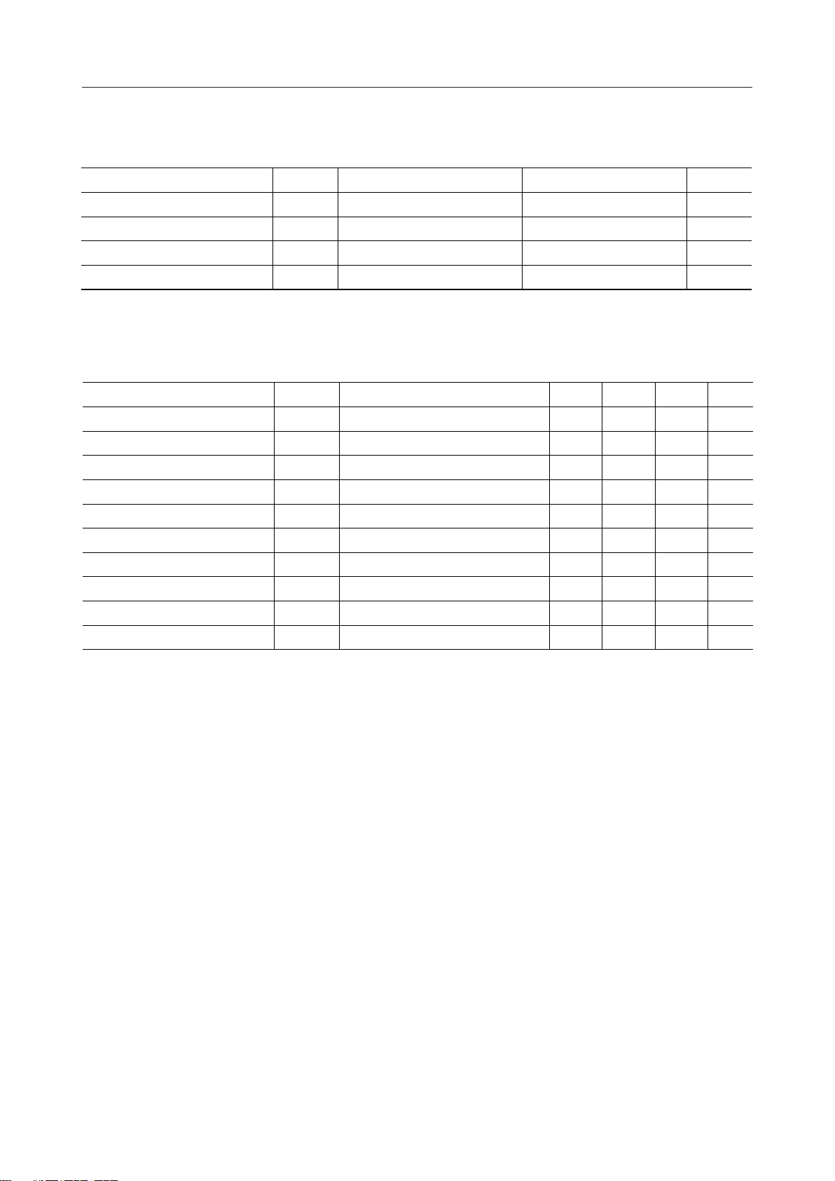
ABSOLUTE MAXIMUM RATINGS
Parameter Symbol Condition Rating Unit
Supply Voltage V
Power Dissipation P
DD
IN
STG
D
—
All inputsInput Voltage V
—Storage Temperature Range T
Ta = 85°C
RECOMMENDED OPERATING CONDITIONS
Parameter Symbol Condition Max. Unit
Supply Voltage V
High Level Input Voltage (1) V
High Level Input Voltage (2) V
High Level Input Voltage (3) V
Low Level Input Voltage (1) V
Low Level Input Voltage (2) V
Clock Frequency f
DD
IH1
IH2
IH3
IL1
IL2
C
OSC
FR
op
All inputs except OSC0, VK
All inputs except OSC0
R = 4.7kW, C=22pFOSC Frequency f
f
OSC
—
VK
OSC0
OSC0
—
= 2 MHzFrame Frequency F
—Operating Temperature Range T
–0.3 to +20 V
–0.3 to +6 V
–65 to +150 °C
0.4 W
Min.
8
3.8
Typ.
—
18 V
5.5 V—
V
DD
5.5 V—4.5
0.8 V—0
0.5 V—0
250 kHz——
— MHz2—
—Hz224—
85 ˚C—–40
V—3.8
6/20
Page 7

¡ Semiconductor MSC1201-xx
ELECTRICAL CHARACTERISTICS
DC Characteristics
Parameter
Hight Level Input Voltage (1)
Hight Level Input Voltage (2)
Hight Level Input Voltage (3)
Low Level Input Voltage (1)
Low Level Input Voltage (2)
Hight Level Input Current (1)
Hight Level Input Current (2)
Hight Level Input Current (3)
Low Level Input Current (1)
Low Level Input Current (2)
Low Level Input Current (3)
High Level Output Voltage (1)
High Level Output Voltage (2) V
Symbol Min. Unit
*1
*9
*2
*10
*2
*3
*4
*5
*3
*4
*5
*6
*7
V
High Level Output Voltage (3)
*8
V
V
*6
Low Level Output Voltage (1)
V
*7
V
Low Level Output Voltage (2)
*8
Power Supply Current
V
IH1
V
IH2
V
IH3
V
IL1
V
IL2
I
IH1
I
IH2
I
IH3
I
IL1
I
IL2
I
IL3
V
OH1
OH2
OH3-1
OH3-2
OL1-1
OL1-2
OL1-3
V
OL2
DD
Condition
V
V
V
V
V
V
V
I
OH1
VDD = 9.5 V
I
OH2
V
I
OH3-1
VDD = 9.5 V
Output Open
V
I
OL1-1
VDD = 9.5 V
I
OL1-2
V
I
OL1-3
VDD = 9.5 V
I
OL2
= 2 MHz, No loadI
f
OSC
—
—
—
—
—
= 5.0 V
IH1
= 5.0 V
IH2
= 5.0 V
IH3
= 0.0 V
IL1
= 0.0 V
IL2
= 0.0 V
IL3
= 9.5 V
DD
= –6 mA
= –30 mA
= 9.5 V
DD
= –200 mA
= 9.5 V
DD
= 500 mA
= 200 mA
= 9.5 V
DD
= 2 mA
= 200 mA
(Ta = –40 to +85˚C, V
3.8
3.8
4.5
0
0
–5
–80
–60
–5
–0.6
–320
-0.8
V
DD
-0.8 V—
V
DD
4
4.5
—
—
—
—
= 8 to 18 V)
DD
Max.
5.5
V
DD
5.5
0.8
0.5
5
80
60
5
–0.1
–30
—
6
6
2
1
0.3
0.8
20
V
V
V
V
V
mA
mA
mA
mA
mA
mA
V
V
V
V
V
V
V—
mA
Notes: *1 Applicable to all input pins (except VK, OSC0 pin)
*2 Applicable to OSC0 pin
*3 Applicable to CLOCK, DATA, CS, VK, and PWMIN pin
*4 Applicable to TEST1
*5 Applicable to INH pin
*6 Applicable to pins SEG1 to SEG30
*7 Applicable to GRID1 and GRID2
*8 Applicable to DATA OUT pin
*9 Applicable to VK pin
*10 Applicable to all input pins (except OSC0 pin)
7/20
Page 8

¡ Semiconductor MSC1201-xx
AC Characteristics
Parameter Symbol Condition Max. Unit
Oscillation Frequency f
OSC0 Input Frequency f
Clock Frequency f
Clock Pulse Width t
Data Set-up Time t
Data Hold Time t
CS Pulse Width t
CS Off Time t
CS Set-up Time
CS-Clock Time
CS Hold Time
Clock-CS Time
Data Output Delay
Clock-Data out Time
SEG & GRID Output Delay
from CS
OSC
OSCI
CW
DS
DH
CSW
CSL
t
CSS
t
CSH
t
PD
t
ODS
(Ta = –40 to +85°C, V
= 8 to 18 V)
DD
Min.
R = 4.7kW, C = 22pF
1.2
External input only
C
—
—
—
—
—
—
—
—
—
C
= 100pF
L
2.8 MHz
2.5 MHz1.5
250 kHz—
— ms1.3
— ms1
—ns200
— ms68
— ms30
— ms2
— ms2
1 ms—
8 ms—
PCS
t
POF
PRZ
t
R
FR
Slew Rate (All Drivers)
Power-off Hold Time
PWM Conversion Characteristics
Parameter
PWM Input Frequency
Input Threshold Voltage
PWM Input Duty Cycle d
Symbol Condition Unit
f
PWM
v
R
U
= 100pF, t = 20% to 80% or
C
L
80% to 20%
—Power-on CS Time t
When the Unit mounted
V
= 0 V
DD
When the Unit mountedPower-on Rise Time t
—Frame Frequency F
—
—
—
(Ta = –40 to +85°C, V
Min.
176
0.8
20
Typ.
256
2.5
—
5 ms—
— ms300
—ms5
100 ms—
342 Hz146
= 8 to 18 V)
DD
Max.
336
3.8
100
Hz
V
%
8/20
Page 9

¡ Semiconductor MSC1201-xx
TIMING DIAGRAM
t
CSW
CS
CLOCK
DATA
3.8V
0.8V
3.8V
0.8V
3.8V
0.8V
DH
f
C
t
CSS
t
CW
t
DS
t
VALID VALID
Fig. 1 Data Input Timing
t
CW
t
CSL
t
CSH
t
DS
t
DH
CLOCK
DATA
3.8V
0.8V
3.8V
0.8V
t
CW
t
PD
t
CW
Fig. 2 Data Output Timing
t
PD
9/20
Page 10

¡ Semiconductor MSC1201-xx
TIMING DIAGRAM (Continued)
V
CS
CS
DD
8V
3.8V
0.8V
3.8V
0.8V
t
PCS
Fig. 3 Power-On Timing
t
ODS
t
R
t
POF
t
CSW
t
PRZ
t
ODS
t
R
SEG1-30
GRID1, 2
PWMIN
80%
20%
Input
Threshold
Voltage
Fig. 4 SEG & GRID Driver Output Timing
PWM Frequency (f
A
) Duty Cycle dU = A/(A+B)
PWM
B
Fig. 5 PWM Input Waveform
10/20
Page 11

¡ Semiconductor MSC1201-xx
FUNCTIONAL DESCRIPTION
Power-On-Reset
The status of the internal circuit after power-on reset is as follows;
1) Shift registers and latches are reset.
2) PWM conversion mode is selected.
DATA Input
Data input is available only when the high level is applied to the "CS" pin. Input data is shifted
into shift registers through "Data" pin at the rising edge of the shift clock. The data is
automatically loaded to latches at the falling edge of "CS" signal. When M0 = "0", input data
should include display data (total of 64 bits data should be input.) and when M0 = "1", input data
should exclude display data (Total of 16-bit data should be input.)
[Data Format]
1) Display Data Input Mode
Input Data : 64 bits
VF Display Data : 60 bits
Mode Select Data : 4 bits
First In
Bit
64
D5963D5862D57
Display
Data
53
D4852M351M250M149M048D47
Mode
Data
3D22D11
D0
Display
Data
2) Segment outputs/Shift Registers Bit Correspondence Table
The content of the table depends on a PLA code.
This table is modeled on the general purpose code of -01.
Segment output positions can be changed dependent on the PLA code, but the segment-bit
correspondence cannot be changed.
302928272625242322212019181716151413121110987654321
302928272625242322212019181716151413121110987654321
Bit
60 59 58 57 56 55 54 53 52 51 50 49 48 47 46 45 44 43 42 41 40 39 38 37 36 35 34 33 32 31
SEGn
GRID1
GRID2
11/20
Page 12

¡ Semiconductor MSC1201-xx
3) Digital Dimming Data Input Mode
Input Data : 16 bits
Digital Dimming Data : 11 bits
Mode Select Data : 4 bits
64 63 621061960859758657556455354253152
xx 11
MSB
Dimming Data
(MSB) INPUT DATA (LSB)
0000000000
X
0000000000
X
1111111000
X
1111111111
X
4) Function Mode
0
1
0
1
LSB
51
M
M
3
2
Mode Data
DUTY CYCLE
0/2048
1/2048
2032/2048
2032/2048
50
M
49
First inBit
M
1
0
Mode
S1
S2 0 0 0 1 Digital Dimming Data Input
S3 0 0 1 0 PWM Conversion Select & Display Data Input
S4 0 0 1 1 PWM Conversion Select
S5 0 1 0 0 Digital Dimming Select & Display Data Input
S6 0 1 0 1 Digital Dimming Select
M3
0 0 0 0 Display Data Input
M2 M1 M0 Function
12/20
Page 13

¡ Semiconductor MSC1201-xx
PWM Conversion
In the PWM conversion mode, "lamp PWM", which is used for dimming control of back-light for
instrument clusters or other displays, is used to generate the PWM signal for VFD tube dimming
control. The lamp PWM input to "PWM IN" pin is converted to PWM signal for VFD tube with
a built-in PWM conversion look-up table (User-Programmable Mask ROM).
The duty cycle of the lamp PWM is defined as follows:
PWMIN
A
PWM Input Frequency = 256 ± 80Hz
Duty Cycle = A / (A+B)
B5V
Note: The duty cycle of the lamp PWM signal is measured with a reference point of 2.5 V typ.
As the reference point of 2.5 V is the threshold voltage of "PWM IN" pin, it deviates to
some value between 0.8 V and 3.8 V due to process parameter deviation. Therefore, the
PWM conversion error increases as the rise/fall time of the lamp PWM increases.
GRID/SEG Driver Operation and Digital/Analog Dimming Operation
Figure 6 shows an output timing of the GRID and SEG Driver when the VK is "H" level.
Output timings of the GRID and SEG drivers are shown in figure 7 for the digital dimming mode
operation in figure 8 for the PWM conversion mode operation.
(1) GRID and SEG drivers output timings when VK = "H"
1 Frame (4096-bit times)
f
FR
GRID1
GRID2
SEG1-30
Fig. 6 GRID and SEG Output Timing (VK = "H")
Note: One bit time = 2/f
6-bit times
= 1 ms typ.
OSC
2032-bit times
2038-bit times
16-bit times
10-bit times
13/20
Page 14

¡ Semiconductor MSC1201-xx
(2) GRID and SEG driver output timing when VK = "L" and in Digital Dimming Mode.
1 Frame (4096-bit times)
f
FR
GRID1
GRID2
SEG1-30
Max.
2032-bit times
6-bit times
Max.
2038-bit times
10-bit times
16-bit times
Fig. 7 GRID and SEG Output Timing (digital dimming mode)
Notes: • The above indicates the timing for the digital dimming mode with the duty cycle of
2032/2048 at V
PARK
= "L" level.
• The On-times for GRID and SEG are specified with the 11 bits of the digital dimming
data.
• One bit time = 2/f
= 1 ms typ.
OSC
(3) GRID and SEG driver output timings when VK = "L" and in PWM Conversion Mode
1 Frame (2048-bit times)
f
FR
GRID1
GRID2
Max.
256-bit times
3-bit times
SEG1-30
Max.
259-bit times
8-bit times
Fig. 8 GRID and SEG Driver Output Timing (PWM conversion mode)
Notes: • The above indicates the GRID and SEG Drivers Timing when the PWM conversion
mode at VK = "L" level is selected.
• One bit time = 4/f
= 2 ms typ.
OSC
14/20
Page 15

¡ Semiconductor MSC1201-xx
PWM Conversion Table
MSC1201-01
STEP No.
0
1
2
3
4
5
6
7
8
9
10
11
12
13
14
15
16
17
18
19
20
21
22
23
24
25
26
27
28
29
30
31
32
LAMP PWM
DUTY CYCLE
98.75%
97.50%
96.25%
95.00%
93.75%
92.50%
91.25%
90.00%
88.75%
87.50%
86.25%
85.00%
83.75%
82.50%
81.25%
80.00%
78.75%
77.50%
76.25%
75.00%
73.75%
72.50%
71.25%
70.00%
68.75%
67.50%
66.25%
65.00%
63.75%
62.50%
61.25%
60.00%
VF PWM
DUTY CYCLE
12.50%100.00%
12.30%
12.11%
11.91%
11.72%
11.52%
11.33%
11.13%
10.94%
10.74%
10.55%
10.35%
10.16%
9.96%
9.77%
9.57%
9.38%
9.18%
8.98%
8.79%
8.59%
8.40%
8.20%
8.01%
7.81%
7.62%
7.42%
7.23%
7.03%
6.84%
6.64%
6.45%
6.25%
STEP No.
33
34
35
36
37
38
39
40
41
42
43
44
45
46
47
48
49
50
51
52
53
54
55
56
57
58
59
60
61
62
63
64
LAMP PWM
DUTY CYCLE
58.75%
57.50%
56.25%
55.00%
53.75%
52.50%
51.25%
50.00%
48.75%
47.50%
46.25%
45.00%
43.75%
42.50%
41.25%
40.00%
38.75%
37.50%
36.25%
35.00%
33.75%
32.50%
31.25%
30.00%
28.75%
27.50%
26.25%
25.00%
23.75%
22.50%
21.25%
20.00%
VF PWM
DUTY CYCLE
6.05%
5.86%
5.66%
5.47%
5.27%
5.08%
4.88%
4.69%
4.49%
4.30%
4.10%
3.91%
3.71%
3.52%
3.32%
3.13%
2.93%
2.73%
2.54%
2.34%
2.15%
1.95%
1.76%
1.56%
1.37%
1.17%
0.98%
0.78%
0.59%
0.39%
0.20%
0.10%
15/20
Page 16

¡ Semiconductor MSC1201-xx
PLA Code Table
MSC1201-01
SEG 1
SEG 2
SEG 3
SEG 4
SEG 5
SEG 6
SEG 7
SEG 8
SEG 9
SEG 10
SEG 11
SEG 12
SEG 13
SEG 14
SEG 15
SEG 16
SEG 17
SEG 18
SEG 19
SEG 20
SEG 21
SEG 22
SEG 23
SEG 24
SEG 25
SEG 26
SEG 27
SEG 28
SEG 29
SEG 30
PIN 24
PIN 25
PIN 26
PIN 27
PIN 28
PIN 29
PIN 30
PIN 31
PIN 32
PIN 33
PIN 34
PIN 35
PIN 36
PIN 37
PIN 38
PIN 39
PIN 40
PIN 41
PIN 42
PIN 43
PIN 44
PIN 1
PIN 2
PIN 3
PIN 4
PIN 5
PIN 6
PIN 7
PIN 8
PIN 9
BIT 1, 31
BIT 2, 32
BIT 3, 33
BIT 4, 34
BIT 5, 35
BIT 6, 36
BIT 7, 37
BIT 8, 38
BIT 9, 39
BIT10, 40
BIT11, 41
BIT12, 42
BIT13, 43
BIT14, 44
BIT15, 45
BIT16, 46
BIT17, 47
BIT18, 48
BIT19, 49
BIT20, 50
BIT21, 51
BIT22, 52
BIT23, 53
BIT24, 54
BIT25, 55
BIT26, 56
BIT27, 57
BIT28, 58
BIT29, 59
BIT30, 60
16/20
Page 17

¡ Semiconductor MSC1201-xx
Pin Name Output Pin Name Output
SEG1 BIT 1,31 SEG16 BIT 16,46
SEG2 BIT 2,32 SEG17 BIT 17,47
SEG3 BIT 3,33 SEG18 BIT 18,48
SEG4 BIT 4,34 SEG19 BIT 19,49
SEG5 BIT 5,35 SEG20 BIT 20,50
SEG6 BIT 6,36 SEG21 BIT 21,51
SEG7 BIT 7,37 SEG22 BIT 22,52
SEG8 BIT 8,38 SEG23 BIT 23,53
SEG9 BIT 9,39 SEG24 BIT 24,54
SEG10 BIT 10,40 SEG25 BIT 25,55
SEG11 BIT 11,41 SEG26 BIT 26,56
SEG12 BIT 12,42 SEG27 BIT 27,57
SEG13 BIT 13,43 SEG28 BIT 28,58
SEG14 BIT 14,44 SEG29 BIT 29,59
SEG15 BIT 15,45 SEG30 BIT 30,60
17/20
Page 18

¡ Semiconductor MSC1201-xx
APPLICATION CIRCUITS
(1) Digital Dimming Mode
1/2 Duty VF Tube
Micro-
controller
12 V
SEG1 SEG30 G1,G2
VDD
GND
CS
DATA
CLOCK
OSC1
OSC0
VK
PWM IN
MSC1201-xx
18/20
Page 19

¡ Semiconductor MSC1201-xx
(2) PWM Conversion Mode
1/2 Duty VF Display Tube
SEG1 SEG30 G1 G2
12 V
V
DD
GND
CS
Micro-
controller
DATA
CLOCK
MSC1201-xx
Daylight Mode "1"
Dark Mode "0"
Illumination Switch
Dashboard Lamp
Lamp PWM Signal
Illumination Lamp
5 V
OSC1
OSC0
VK
PWMIN
19/20
Page 20

¡ Semiconductor MSC1201-xx
PACKAGE DIMENSIONS
(Unit : mm)
QFP44-P-910-0.80-2K
Mirror finish
Package material
Lead frame material
Pin treatment
Solder plate thickness
Package weight (g)
Epoxy resin
42 alloy
Solder plating
5 mm or more
0.41 TYP.
Notes for Mounting the Surface Mount Type Package
The SOP, QFP, TSOP, SOJ, QFJ (PLCC), SHP and BGA are surface mount type packages, which
are very susceptible to heat in reflow mounting and humidity absorbed in storage.
Therefore, before you perform reflow mounting, contact Oki’s responsible sales person for the
product name, package name, pin number, package code and desired mounting conditions
(reflow method, temperature and times).
20/20
 Loading...