

Page 1
Cascadable Silicon Bipolar
MMIC␣ Amplifier
Technical Data
MSA-9970
Features
• Open Loop Feedback
Amplifier
• Performance Flexibility with
User Selected External
Feedback for:
Broadband Minimum
Ripple Amplifiers
Low Return Loss
Amplifiers
Negative Gain Slope
Amplifiers
• Usable Gain to 6.0 GHz
• 16.0 dB Typical Open Loop
Gain at 1.0 GHz
• 14.5 dBm Typical P
1dB
at
1.0␣ GHz
• Hermetic Gold-ceramic
Microstrip Package
The MSA-9970 is a high performance silicon bipolar Monolithic
Microwave Integrated Circuit
(MMIC) housed in a hermetic high
reliability package. This MMIC is
designed with high open loop gain
and is intended to be used with
external resistive and reactive
feedback elements to create a
variety of special purpose gain
blocks.
Applications include very broadband, minimum ripple amplifiers
with extended low frequency
performance possible through the
use of a high valued external
feedback blocking capacitor;
extremely well matched (–20 dB
return loss) amplifiers; and
negative gain slope amplifiers for
flattening MMIC cascades.
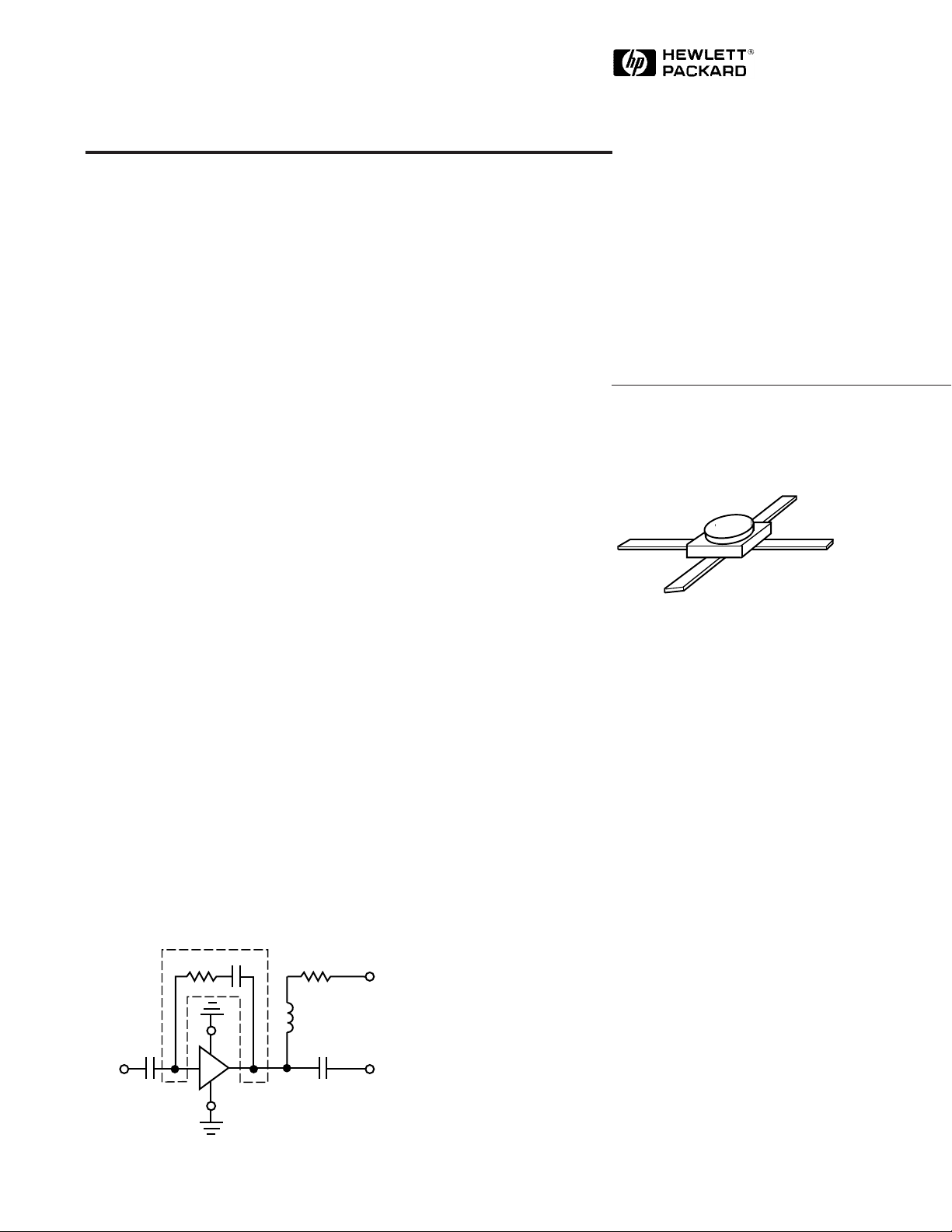
Typical Biasing Configuration
USER SELECTABLE
C
f
R
f
R
bias
70 mil PackageDescription
The MSA-series is fabricated using
HP’s 10 GHz fT, 25␣ GHz f
silicon bipolar MMIC process
which uses nitride self-alignment,
ion implantation, and gold metallization to achieve excellent
performance, uniformity and
reliability. The use of an external
bias resistor for temperature and
current stability also allows bias
flexibility.
V
≥ 10 V
CC
MAX
,
RFC (Optional)
C
block
IN
4
3
MSA
1
2
Vd = 7.8 V
C
block
OUT
6-489
5965-9668E
Page 2
MSA-9970 Absolute Maximum Ratings
Parameter Absolute Maximum
Device Current 80 mA
Power Dissipation
RF Input Power +13 dBm
Junction Temperature 200°C
Storage Temperature –65°C to 200°C
Notes:
1. Permanent damage may occur if any of these limits are exceeded.
2. T
3. Derate at 6.7 mW/° C for T
4. The small spot size of this technique results in a higher, though more
= 25°C.
CASE
accurate determination of θ
MENTS section “Thermal Resistance” for more information.
[2,3]
750 mW
> 88° C.
C
than do alternate methods. See MEASURE-
jc
[1]
Thermal Resistance
θjc = 150°C/W
[2,4]
:
Electrical Specifications
Symbol Parameters and Test Conditions: Id = 35 mA, Z
G
P
Power Gain
[2]
(|S21|2) f = 0.1 GHz dB 17.5
[1]
, T
A
= 25° C
= 50 Ω Units Min. Typ. Max.
O
f = 1.0 GHz 14.5 16.0 17.5
f = 4.0 GHz 8.0 9.0 10.0
P
IP
V
1 dB
3
d
Output Power at 1 dB Gain Compression
Third Order Intercept Point
[2]
Device Voltage V 7.0 7.8 8.6
[2]
f = 1.0 GHz dBm 14.5
f = 1.0 GHz dBm 25.0
dV/dT Device Voltage Temperature Coefficient mV/°C –16.0
Notes:
1. The recommended operating current range for this device is 25 to 45 mA. Typical performance as a function of current
is on the following page.
2. Open loop value. Adding external feedback will alter device performance.
6-490
Page 3

MSA-9970 Typical Scattering Parameters (Z
G
p
(dB)G
p
(dB)
G
p
(dB)
0.3.05 0.1 0.5 1.0 3.0 6.0
FREQUENCY (GHz) FREQUENCY (GHz)
Figure 1. Open Loop Power Gain vs.
Frequency, I
d
= 35 mA.
0.20.1 0.3 0.5 1.0 2.0 4.0
Figure 3. Open Loop Output Power at
1 dB Gain Compression vs. Frequency.
0
3
6
9
12
15
18
21
7
9
11
15
13
19
17
Figure 4. Open Loop Power Gain vs.
Current.
5
10
15
20
–55 +25–25 +125+85
P
1 dB
(dBm)
P
1 dB
(dBm)
TEMPERATURE (°C)
2046108
V
d
(V)
Figure 2. Device Current vs. Voltage.
0
10
20
30
50
40
I
d
(mA)
TC = +125°C
T
C
= +25°C
TC = –55°C
Figure 5. Open Loop Output Power at
1 dB Gain Compression and Open Loop
Power Gain vs. Case Temperature,
f=1.0 GHz, I
d
= 35 mA.
13
14
15
16
17
Id = 45 mA
Id = 35 mA
Id = 25 mA
2010 30 40 50
I
d
(mA)
0.1 GHz
1.0 GHz
4.0 GHz
P
1 dB
G
p
Freq.
S
11
S
21
= 50 Ω, TA = 25° C, I
O
S
12
S
= 35 mA)
d
22
GHz Mag Ang dB Mag Ang dB Mag Ang Mag Ang k
0.02 .89 –1 17.5 7.51 179 –37.2 .014 4 .93 –1 1.01
0.05 .90 –3 17.5 7.47 177 –35.6 .017 34 .92 –3 .83
0.1 .90 –6 17.4 7.45 174 –33.2 .022 43 .93 –6 .70
0.2 .89 –12 17.4 7.43 168 –29.6 .033 61 .93 –13 .39
0.4 .87 –24 17.2 7.27 156 –24.4 .061 63 .91 –27 .24
0.6 .85 –36 17.0 7.06 145 –20.8 .091 58 .90 –40 .21
0.8 .82 –47 16.6 6.78 134 –18.8 .115 52 .87 –53 .21
1.0 .79 –59 16.2 6.49 124 –17.0 .141 44 .84 –66 .24
1.5 .72 –86 15.3 5.79 100 –14.6 .186 29 .74 –96 .28
2.0 .65 –113 14.2 5.10 77 –13.4 .215 16 .64 –123 .34
2.5 .59 –133 13.0 4.45 61 –12.9 .227 7 .57 –143 .39
3.0 .54 –155 11.6 3.79 42 –12.5 .236 –3 .51 –163 .46
3.5 .53 –174 10.3 3.28 26 –12.4 .239 –14 .45 178 .53
4.0 .52 168 9.2 2.87 10 –12.5 .238 –22 .39 164 .59
4.5 .53 152 8.0 2.51 –4 –12.6 .234 –30 .34 155 .66
5.0 .55 140 6.9 2.21 –17 –12.8 .228 –37 .31 153 .72
5.5 .55 130 5.8 1.94 –31 –13.2 .220 –44 .30 154 .80
6.0 .55 121 4.6 1.70 –43 –13.6 .209 –48 .32 157 .88
6.5 .56 114 3.5 1.50 –53 –13.8 .203 –54 .37 158 .94
7.0 .56 107 2.6 1.34 –63 –14.0 .201 –59 .42 157 .97
A model for this device is available in the DEVICE MODELS section.
Typical Performance, T
(unless otherwise noted)
= 25° C
A
6-491
Page 4

70 mil Package Dimensions
.040
1.02
42GROUND
RF OUTPUT
RF INPUT
AND BIAS
.020
.508
1
.004 ± .002
.10 ± .05
GROUND
.070
1.70
.495 ± .030
12.57 ± .76
3
Notes:
(unless otherwise specified)
1. Dimensions are
2. Tolerances
in .xxx = ± 0.005
mm .xx = ± 0.13
.035
.89
in
mm
6-492
 Loading...