

Page 1

E2A0032-16-X0
¡ Semiconductor MSA4709A
¡ Semiconductor
This version: Jan. 1998
Previous version: Nov. 1996
MSA4709A
Subscriber Line Interface Circuit
GENERAL DESCRIPTION
The MSA4709A is designed to provide BSH functions and to meet PABX transmission performance
requirements.
This device provides two-wire to four-wire conversion function (Hybrid).
FEATURES
• B (Battery feed), S (Supervision), and H (Hybrid) functions integrated on chip.
• Design to meet Central Office and PABX quality transmission requirements.
• All transmission performance parameters can be externally programmable.
• Free from parasitic SCR's using dielectric isolation technology.
• Size and weight reduction over conventional approaches.
• Supply voltage selectable (V
• 1 channel built-in relay driver.
• Package:
30-pin plastic Shrink DIP (SDIP30-P-400-1.78) (Product name: MSA4709ASS)
= –24 V/–48 V).
BB
1/11
Page 2
¡ Semiconductor MSA4709A
2/11
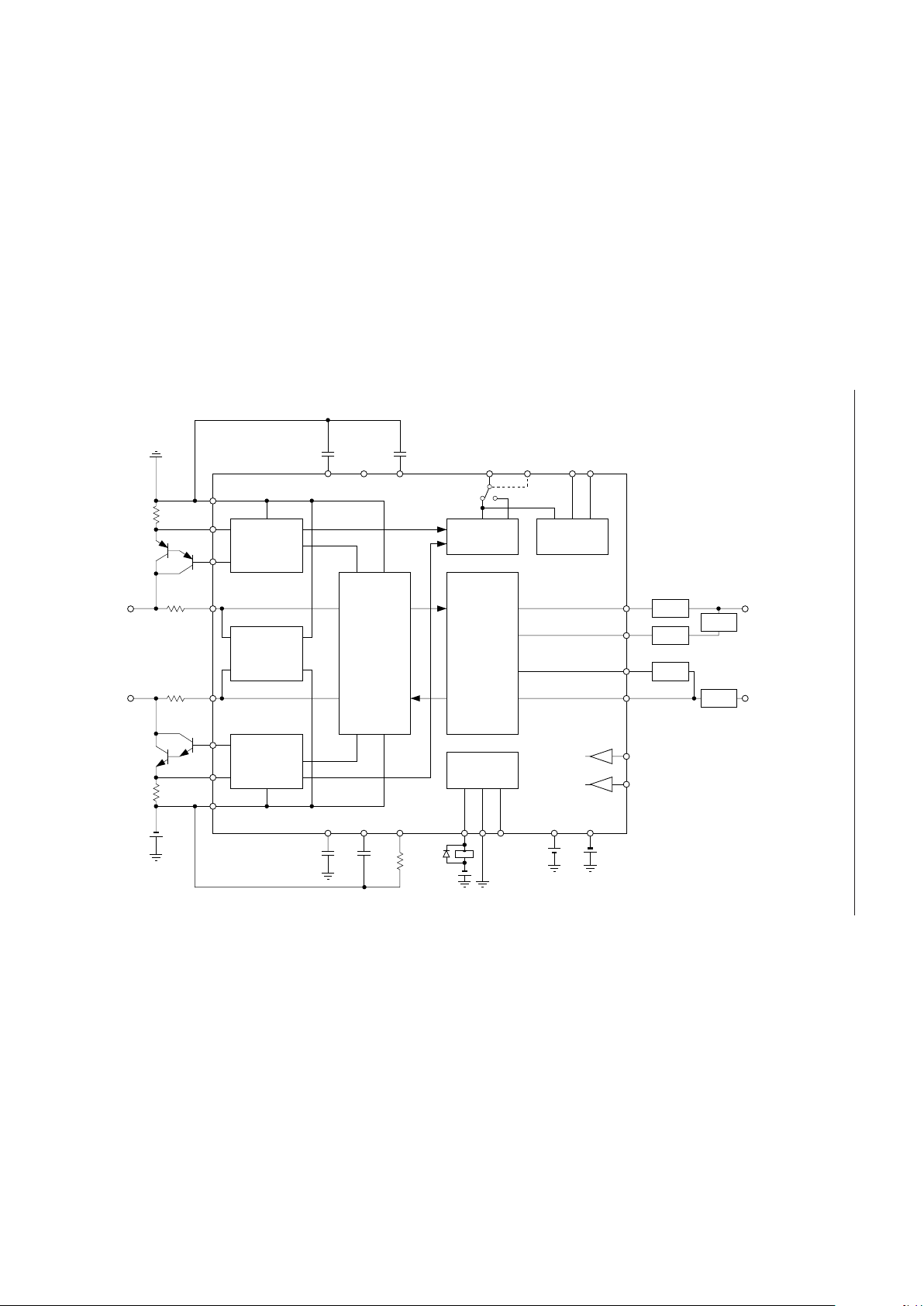
BLOCK DIAGRAM
Ring Current
DET
Ring Current
Drive Amp.
Over Voltage
Protection
TIP Current
DET
TIP Current
Drive Amp.
Interface
Circuit
HYB
Loop & Fault
DET
RING TRIP
Relay Driver
TIP
RING
Z
t
Z
FR
Z
R
Z
b
4WR
ZR
BN
ZX
4WS
4WR
Z
X
VBS
BF
SCN SEL RG RB
V
EE
V
CC
RI
RSI
RSO
V
BB
or
V
EE
RY
CDC
CN
V
BB
NE
NB
A
B
PB
PE
G
CB IL
CDP
Page 3
¡ Semiconductor MSA4709A
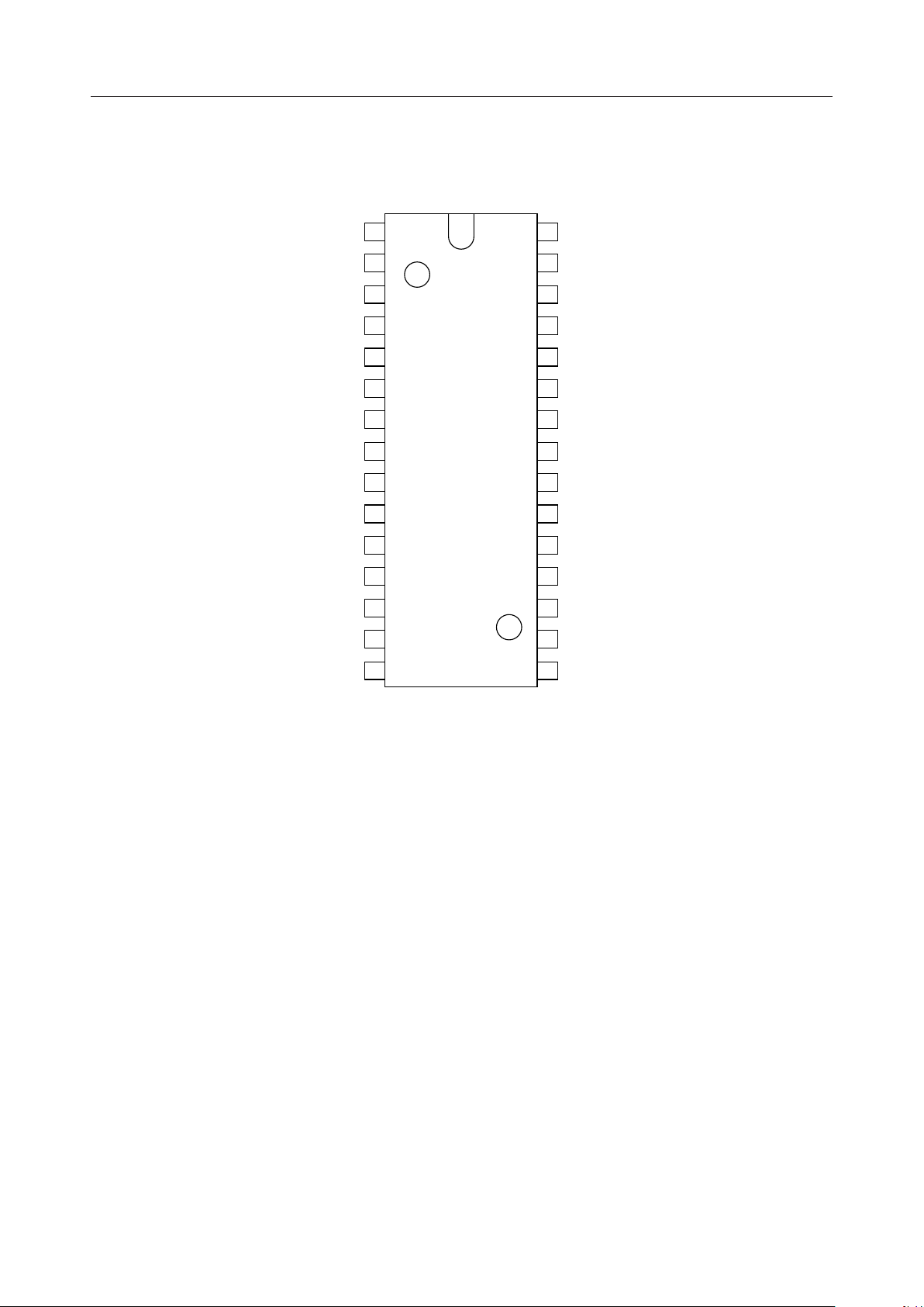
PIN CONFIGURATION (TOP VIEW)
30
29
28
27
26
25
24
NC
B
PE
PB
G
CB
ZX
V
BB
NE
NB
RSO
CN
RY
1
2
A
3
4
5
6
7
Note: NC: No connect pin
CDC
8
RSI
9
RB
10
RG
11
V
12
EE
13
4WR
14
BN
15 16
ZR
30-Pin Plastic Shrink DIP
23
22
21
20
19
18
17
V
CC
RI
BF
VBS
IL
CDP
SEL
SCN
3/11
Page 4
¡ Semiconductor MSA4709A
PIN DESCRIPTION
Pin No. Name Description
1VBBBattery supply, –48 V or –24 V input.
2A
3NE
4 NB The base drive output for the NPN Darlington transistor.
5 RSO Relay driver current sink terminal.
6 CN Battery noise rejection capacitor input. This capacitor value is 1 mF (60V).
7 RY AC performance adjusting resistor RY input.
8 CDC
9 RSI Relay driver current source terminal.
10 RB Ring-Trip filtering capacitor input (RING).
11 RG Ring-Trip filtering capacitor input (TIP).
12 V
13 4WR
14 BN Balancing network drive output.
15 ZR Receive gain adjust and frequency compensation input.
EE
The Ring voltage sensing input. This input is high impedance (apr. 37 kW), and is
connected to the built-in over voltage protection circuit.
The Ring current sensing input is connected to the emitter of NPN Darlington transistor
and the power resistor REA.
AC high impedance providing capacitor Cdc input and constant current feed at the short
line adjusting zener diode input. This capacitor value is 1 mF (15V).
–5 V input.
Receive input and is connected to the negative input of the built-in buffer operational
amplifier.
Output of both the fault current detector and loop current detector. This output is opencollector with a built-in pull-up resistor. (apr. 10 kW).
16 SCN
Condition SEL = "H" SEL = "L"
• ON-Hook H H
• OFF-Hook L H
• Dial pulse: break H H
• Dial pulse: make L H
• RING TRIP L H
• Ground/Battery fault L L
4/11
Page 5

¡ Semiconductor MSA4709A
Pin No. Name Description
17 SEL
18 CDP Dial pulse shaping capacitor input.
19 IL Tip to Ring constant loop current determination resistor input.
20 VBS
21 BF
22 RI Relay driver control input. RI = "H" is Driver "ON"
23 V
CC
24 ZX
25 CB
26 G Ground input.
27 PB The base drive output for the PNP Darlington power transistor.
28 PE
29 B
30 NC No connection
SCN output information select control input. At SEL = "L", SCN Indicates only ground/
battery fault condition.
Supply voltage selection terminal.
V
= VCC (–24 V), VBS = G (–48 V).
BS
Battery-feed mode control input. A logic level "H" switches off both the Ring and Tip
current drive amp. and presents a high impedance to the line. (apr. 80 kW).
+5 V input
2 wire terminating impedance compornent Zx input. This pin has a low input
impedance.
Compensation capacitor input.
This capacitor value is 4700 pF(35V).
The Tip current sensing input is connected to the emitter of the PNP Darlington power
transister and the power resistor REB.
The Tip voltage sensing input. This input is high impedance (apr. 37 kW) and is
connected to the built-in over voltage protection circuit.
5/11
Page 6

¡ Semiconductor MSA4709A
ABSOLUTE MAXIMUM RATINGS
(Ta = 25°C)
Parameter Unit
Symbol Condition
VBS = G
V
BB
Power Supply Voltage
CC
EE
IN
RD
op
STG
VBS = V
— –0.3 to +7.0V
— –7.0 to +0.3V
— –0.3 to VCC + 0.3V
VRI = H –30I
— 0 to 80T
— –55 to 150T
RECOMMENDED OPERATING CONDITIONS
Parameter Max. Unit
Power Supply Voltage
Loop Resistance
Symbol Condition
VBS = G
V
BB
CC
EE
R
L
CC
CC
Rating
–53.0 to +0.3
–30.0 to +0.3
Typ.Min.
–53
–30VBS = V
–48 –43
–24 –21.6
+4.75— +5 +5.25V
–5.25— –5 –4.75V
0VBB = –48 V — 2000
0VBB = –24 V — 600
0——70TaOperating Ambient Temperature °C
V
VDigital Input Voltage
mARelay Driver Current
°COperating Temperature
°CStorage Temperature
V
W
6/11
Page 7

¡ Semiconductor MSA4709A
ELECTRICAL CHARACTERISTICS
DC Characteristics
(I
= 30 mA, VBB = –24/–48 V, VCC = 5 V, VEE = –5 V, Ta = 25°C)
L
Parameter Max. Unit
Power Supply Current
Power Dissipation
Loop Current mA
Symbol Condition
I
BB
CC
EE
BB
CC
EE
I
BB
CC
EE
BB
CC
EE
VBB = –24 V
ON-HOOK
V
= –24 V
BB
OFF-HOOK
V
= –48 V
BB
ON-HOOK
V
= –48 V
BB
OFF-HOOK
VBB = –24 V
ON-HOOK
V
= –24 V
BB
OFF-HOOK
V
= –48 V
BB
ON-HOOK
V
= –48 V
BB
OFF-HOOK
RSI-RSO
I
= 30 mARelay Driver Output Voltage V
RSI-RSO
—
— 4.0 6.0I
— 1 1.5I
—
— 5.4 8.1I
— 1.2 1.8I
—
— 4.0 6.0I
— 1 1.5I
—
— 6.1 9.2I
— 1.2 1.8I
— 70 100Pds24
— 130 200Pd24
— 100 150Pds48
— 280 420Pd48
26 30 34IL50 RL = 50 W
26 30 34IL400 RL = 400 W
———IL1K RL = 1 kW
–3 — 1.2V
Typ.Min.
1.7 2.6
mA
3.7 6.2I
1.5 2.3
mA
5.0 7.5I
mW
7/11
Page 8

¡ Semiconductor MSA4709A
AC Characteristics
( V
= –24/–48 V, VCC = 5 V, VEE = –5 V, Ta = 25°C )
BB
Parameter Max. Unit
Transmit &
Receive Gain
Insertion Loss
Variety
Idel Channel Noise
Signal to Distortion
Ratio
Longitudinal
Balance
AC Induction
Tolerance
Power Supply
Rejection Ratio
2WÆ4W
4WÆ2W
2WÆ4W
4WÆ2W
2W
4W
2WÆ4W
4WÆ2W
2W
4W
2WÆ4W
4WÆ2W
VBBÆ2W
VCCÆ2W
VEEÆ2W
VBBÆ4W
VCCÆ4W
VEEÆ4W
Symbol Condition
G
DL
SN
LB
NI
24
42
24
42
2
4
24
42
2W
4W
= 0 dBm0
V
i
f = 1 kHz
f = 0.3 to 3.4 kHz
Vi = –55 to +3 dBm0
Psohometric Filter
f = 1 kHz
Vi = 0 dBm0
f = 0.3 kHz to 3.4 kHz
f = 0.3 kHz to 3.4 kHz
f = 0.3 kHz to 3.4 kHz
I
AC24
AC42
2
2
2
4
4
4
= 12.8 mArms
I
AC
Vi = 0 dBm0
f = 0.3 kHz to 3.4 kHz
Vin = 24.5 mVrms
f = 0.3 kHz to 3.4 kHz
Vin = 24.5 mVrms
—
— –4.0 —G
–0.1
–0.1 — 0.1DL
—
— — –81NI
53
53 — —SN
40
40 — —LB
20
23
53
53 — —I
20 — —LB
20 — —LC
20 — —LE
20 — —LB
20 — —LC
20 — —LE
Typ.Min.
4.0 —
— 0.1
— –81
——
——
——LMReturn Loss dB
——LRTranshybrid Loss dB
——
dB
dB
dBm0P
dBP
dB
dB
P
dB
dB
8/11
Page 9

¡ Semiconductor MSA4709A
APPLICATION CIRCUIT
•VBB : –48 V
• Loop Current IL : 30 mA
• Equivalent Terminal Impedance : 600W + 1mF
TIP
RING
750W
(*3)
r
1
(*6)
r
1
750W
V
BB
510k
(*5)
51W
(*1)
(*1)
51W
(*5)
V
BB
(*2)
R1
V
V
BB
–
+
2.2k
2.2k
or V
BB
EE
(*4)
1m
RB VBSVCCVEEIL
G CDC
PE
PB
BBN
AZR
NB
NE
V
BB
RG
RSI
RSO
RI BF SEL SCN
+5V –5V
MSA4709A
(Controller)
27k
RY
ZX
4WR
CDP
CB
CN
1m
–+
4.7k
0.028m
0.028m
2.7k
1m
–+
1m
21k
42k
V
BB
187k
12k
4700pF
GSX
AIN–
AIN+
MSM6999
AOUT+
CODEC
PCM
OUT
PCM
FHW
IN
BHW
750
V
CC
R1
RSI
RSO
RI
TIP
RING
r
1
750W
V
Fig. 1 Fig. 2
BB
510k
+
1m
–
RG
RB
V
BB
9/11
Page 10

¡ Semiconductor MSA4709A
Notes: *1. Use heat sinks required for Darlinton-connected power transistors.
*2. This diagram indicates that VBB or VEE (negative supply) is used for driving the
relay, but a positive supply, such as VEE indicated in Fig. 2, can also be used.
*3. This diagram indicates that the ring trip circuit consists of the RING line connected
to ground through the riging current source and the TIP line connected to the
battery (VBB), but the ring trip circuit can also be configured, using the RG pin
indicated in Fig. 2, by the RING line connected to the battery through the ringing
current source and the TIP line connected to ground.
*4. This diagram indicates VBB=–48V. If –24V is used for VBB, connect the VBS pin to
VCC and change the ring trip filtering constants from 510 kW plus 1 mF to 150 kW plus
33 mF.
*5. Use a resistor with precision of 0.1% or better.
*6. Connect additional circuits for suppressing or absorbing surge and noise caued by
relay contacts.
Battery Feed Characteristics
40
30
(mA)
L
IL = 30 mA
20
Loop Current I
10
0
= –48V
V
BB
= 40 mA
I
L
12
Loop Resistance RL (kW)
40
30
(mA)
L
20
Loop Current I
10
0
Loop Resistance RL (kW)
V
= –24V
BB
10.5 1.5
10/11
Page 11

¡ Semiconductor MSA4709A
PACKAGE DIMENSIONS
(Unit : mm)
SDIP30-P-400-1.78
Package material
Lead frame material
Pin treatment
Solder plate thickness
Package weight (g)
Epoxy resin
42 alloy
Solder plating
5 mm or more
1.80 TYP.
11/11
 Loading...