

Page 1
Silicon Bipolar RFIC Amplifiers
Technical Data
MSA-31XX Series
Features
MSA-3111
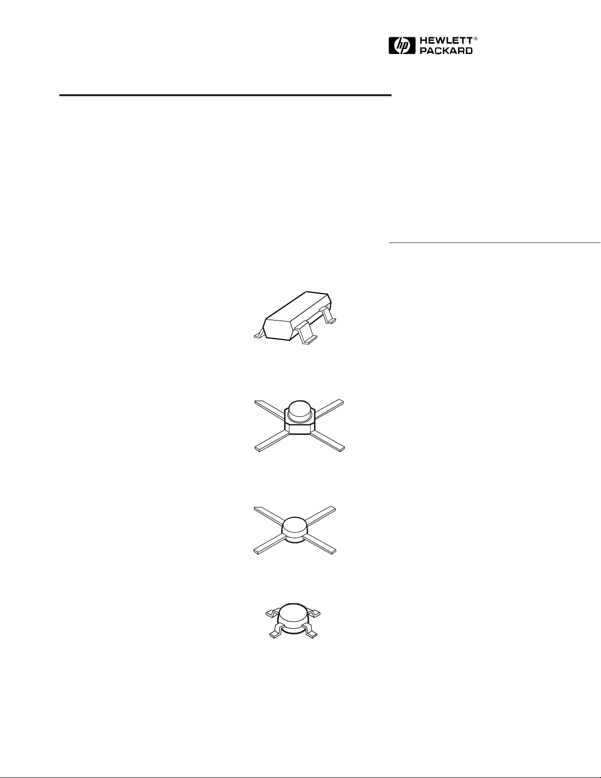
• Surface Mount SOT-143
Package
• 3 dB Bandwidth: DC to
0.5 GHz
• 18.4 dB Gain at 1 GHz
• 3.5 dB NF at 1 GHz
MSA-3135
• Hermetic Ceramic Package
• 3 dB Bandwidth: DC to
0.6 GHz
• 19.6 dB Gain at 1 GHz
• 3.2 dB NF at 1 GHz
MSA-3185
• Plastic Microstrip Package
• 3 dB Bandwidth: DC to
0.5 GHz
• 18.7 dB Gain at 1 GHz
• 3.5 dB NF at 1 GHz
MSA-3186
• Surface Mount Plastic
Microstrip Package
• 3 dB Bandwidth: DC to
0.5 GHz
• 18.7 dB Gain at 1 GHz
• 3.5 dB NF at 1 GHz
MSA-3111
MSA-3135
MSA-3185
MSA-3186
Description
The MSA-31XX series are high
performance silicon bipolar RFIC
amplifiers designed to be
cascadable in 50 Ω systems. The
stability factor of K > 1 contributes to easy cascading in
numerous narrow and broadband
IF and RF commercial and
industrial applications.
The MODAMP MSA series is
fabricated using a 10 GHz fT,
25 GHz F
process which utilizes nitride selfalignment, ion implantation, and
gold metallization to achieve
excellent uniformity,
performance, and reliability. The
use of an external bias resistor for
temperature and current stability
also allows bias flexibility.
Package options include, the
industry standard plastic surface
mount SOT-143 package, the
100␣ mil surface mountable
hermetic ceramic package, the
85␣ mil plastic microstripline
package, and the 85 mil surface
mountable plastic microstripline
package.
, silicon bipolar RFIC
MAX
5965-9664E
6-482
Page 2
Absolute Maximum Ratings
[1]
MSA- MSA- MSA-
Parameter 3111 3135 3185, -3186
Device Current 50 mA 60 mA 60 mA
Power Dissipation
[2,3]
250 mW
[3a]
325 mW
[3b]
325 mW
RF Input Power +13 dBm +13 dBm +13 dBm
Junction Temperature 150°C 200°C 150°C
Storage Temperature -65 to 150°C -65 to 200°C -65 to 150°C
Thermal
Resistance: θ
jc
Notes:
1. Permanent damage may occur if any of these limits are exceeded.
2. T
= 25°C.
CASE
3a. Derate at 2.0 mW/°C for TC > 25°C.
b. Derate at 6.5 mW/°C for TC > 149°C.
c. Derate at 8.7 mW/°C for TC > 112°C.
500°C/W 155°C/W 115°C/W
[3c]
Typical Biasing Configuration
DC BLOCK
INPUT
4
3
MSA
1
V = 4.5 V
d
2
R =
RF CHOKE
bias
R
bias
V – V
CC d
I
d
V 7 V
OUTPUT
CC
Electrical Specifications, T
ID = 29 mA, Z
= 50 Ω
o
= 25°C
A
MSA-3111 MSA-3135 MSA-3185, -3186
Parameters and
Symbol Test Conditions Units Min. Typ. Max. Min. Typ. Max. Min. Typ. Max.
G
P
Power Gain
|2)
(|S
21
f = 0. 1 GH z d B 23.5 24.4 23.5 24.5 26.5 23.5 24.6
f = 0. 5 GH z 22.4 22.8 22.3
f = 1. 0 GH z 18.4 19.6 18.7
∆G
P
Gain Flatness
f = 0.1 to 0.3 GHz d B ±0.5 ± 0.4 ± 1.0 ± 0.5
f
3dB
3 dB Bandwidth GHz 0.5 0.6 0.5
VSWR Input VSWR
f = 0.1 to 3.0 GHz 1.2:1 1.2:1 1.2:1
Output VSWR
f = 0.1 to 3.0 GHz 1.2:1 1.2:1 1.4:1
P
1dB
Power Output @
1 dB Gain
Compression:
f = 1.0 GHz dBm 9.0 9.3 9.0
NF 50 Ω Noise
Figure
f = 1.0 GHz dB 3.5 3.2 3.5
IP
3
Third Order
Intercept
Point
f = 1.0 GHz dBm 23 22 21
t
Group Delay
d
f = 1.0 GHz psec 130 130 130
V
D
Device Voltage
T
= 25°C V 4.0 4.5 6.0 4.5 4.7 5.5 4.0 4.7 6.0
C
dV/dT Device Voltage
Temperature Coefficient mV/°C -9.6 -9.6 -9.6
Note: 1. Refer to “Tape and Reel Packaging for Surface Mount Devices.”
6-483
Page 3

Typical Performance for MSA-3111
z
D
30
25
-55°C
20
-25°C
25°C
85°C
Gp (dB)
15
10
5
0.1 1.0 4.0
FREQUENCY (GHz)
Figure 1. Power Gain vs. Frequency at
Four Temperatures, ID = 29 mA.
30
28
26
24
22
20
Gp (dB)
18
16
14
12
10
20 35
Figure 2. Power Gain vs. Current at
25°C.
0.1 GH
0.5 GHz
1.0 GHz
2.0 GHz
I (mA)
D
14
40 mA
12
35 mA
10
30 mA
8
25 mA
6
1dB
P (dBm)
4
20 mA
2
4025 30
0
0.1
FREQUENCY (GHz)
Figure 3. Typical P
25°C.
1.0 4.0
vs. Frequency at
1dB
5
40 mA
4
NOISE FIGURE (dB)
3
0.1
FREQUENCY (GHz)
20 mA
1.0 4.0
Figure 4. Noise Figure vs. Frequency
at ID = 29 mA.
19
18
GAIN (dB)
17
16
10
1dB
P (dBm)
9
8
-25
Figure 5. Power Gain, Noise Figure,
and P
1dB
ID = 29 mA.
Typical Scattering Parameters at T
ID = 29 mA, Z
Frequency
= 50 Ω
o
S
11
G
P
6
5
4
NF
P
1dB
AMBIENT TEMPERATURE (°C)
3
8525
vs. Temperature at 1 GHz and
= 25°C, for MSA-3111
A
S
21
40
30
20
D
I mA
NOISE FIGURE (dB)
10
0
0
165432
Figure 6. ID vs. VD at Four
Temperatures.
S
12
-55°C
-25°C
25°C
85°C
V (VOLTS)
(GHz) Mag. Ang. (dB) Mag. Ang. (dB) Mag. Ang. Mag. Ang.
0.1 0.05 3 24.4 16.53 167 -27.0 0.045 9 0.10 -23
0.2 0.06 4 24.0 15.83 156 -26.5 0.047 16 0.10 -41
0.3 0.07 -4 23.4 14.78 146 -26.0 0.050 23 0.10 -59
0.4 0.07 -8 22.7 13.59 136 -25.3 0.054 28 0.11 -72
0.5 0.07 -12 22.0 12.53 128 -24.6 0.059 33 0.11 -84
0.6 0.07 -18 21.1 11.41 121 -23.9 0.064 36 0.11 -94
0.7 0.07 -22 20.4 10.47 114 -23.1 0.070 39 0.11 -100
0.8 0.08 -26 19.7 9.63 109 -22.4 0.076 41 0.11 -106
0.9 0.08 -32 19.0 8.89 104 -21.7 0.082 42 0.11 -111
1.0 0.08 -35 18.4 8.27 99 -21.1 0.088 43 0.11 -114
1.5 0.08 -59 15.6 5.99 80 -18.5 0.118 44 0.11 -123
2.0 0.10 -79 13.4 4.69 65 -16.6 0.148 42 0.10 -122
2.5 0.10 -104 11.8 3.88 52 -15.2 0.175 38 0.11 -118
3.0 0.10 -129 10.4 3.31 39 -14.1 0.198 33 0.12 -114
3.5 0.12 -163 9.3 2.91 27 -13.2 0.219 28 0.12 -117
4.0 0.15 164 8.2 2.58 16 -12.6 0.236 23 0.13 -125
4.5 0.21 140 7.4 2.34 4 -12.1 0.250 18 0.13 -136
5.0 0.29 121 6.5 2.10 -7 -11.7 0.260 14 0.14 -148
5.5 0.36 109 5.6 1.90 -18 -11.3 0.271 10 0.17 -158
6.0 0.42 98 4.6 1.70 -28 -11.0 0.282 7 0.21 -165
S
22
6-484
Page 4

Typical Performance for MSA-3135
z
D
30
25
-55°C
20
25°C
85°C
125°C
15
Gp (dB)
10
5
0
0.1
1.0 4.0
FREQUENCY (GHz)
Figure 1. Power Gain vs. Frequency at
Four Temperatures, ID = 29 mA.
30
28
26
24
22
20
Gp (dB)
18
16
14
12
10
20 35
Figure 2. Power Gain vs. Current at
25°C.
0.1 GH
0.5 GHz
1.0 GHz
2.0 GHz
I (mA)
D
16
14
12
10
1dB
P (dBm)
8
6
4025 30
4
0.1 1.0 4.0
Figure 3. Typical P
25°C.
40 mA
35 mA
30 mA
25 mA
20 mA
FREQUENCY (GHz)
vs. Frequency at
1dB
5
4
20 mA
3
NOISE FIGURE (dB)
40 mA
2
0.1 1.0 4.0
FREQUENCY (GHz)
Figure 4. Noise Figure vs. Frequency
at ID = 29 mA.
19
18
GAIN (dB)
17
16
10
1dB
P (dBm)
9
8
-25
Figure 5. Power Gain, Noise Figure,
and P
1dB
ID = 29 mA.
Typical Scattering Parameters at T
ID = 29 mA, Z
Frequency
= 50 Ω
o
S
11
G
P
6
5
4
NF
P
1dB
AMBIENT TEMPERATURE (°C)
3
8525
vs. Temperature at 1 GHz and
= 25°C, for MSA-3135
A
S
21
50
40
30
D
I mA
20
NOISE FIGURE (dB)
10
0
0
125°C
85°C
25°C
-55°C
165432
V (VOLTS)
Figure 6. ID vs. VD at Four
Temperatures.
S
12
(GHz) Mag. Ang. (dB) Mag. Ang. (dB) Mag. Ang. Mag. Ang.
0.1 0.05 1 24.7 17.11 169 -27.3 0.043 7 0.09 -19
0.2 0.06 2 24.4 16.52 158 -27.0 0.045 14 0.09 -37
0.3 0.07 -2 23.9 15.72 149 -26.5 0.047 20 0.09 -52
0.4 0.07 -7 23.4 14.77 139 -26.0 0.050 24 0.09 -67
0.5 0.07 -12 22.8 13.77 131 -25.4 0.054 29 0.09 -80
0.6 0.07 -21 22.1 12.79 124 -24.7 0.058 32 0.09 -92
0.7 0.07 -27 21.5 11.86 117 -24.1 0.063 34 0.09 -102
0.8 0.07 -33 20.9 11.03 111 -23.4 0.037 36 0.09 -111
0.9 0.08 -39 20.2 10.25 106 -22.8 0.072 38 0.09 -119
1.0 0.08 -44 19.6 9.55 101 -22.2 0.078 39 0.09 -127
1.5 0.08 -79 16.9 7.03 80 -19.7 0.104 39 0.10 -155
2.0 0.09 -116 14.8 5.52 63 -17.7 0.130 36 0.10 -171
2.5 0.11 -145 13.2 4.55 49 -16.3 0.153 31 0.09 176
3.0 0.15 -172 11.7 3.86 35 -15.2 0.175 25 0.10 162
3.5 0.19 166 10.5 3.34 22 -14.3 0.192 19 0.11 154
4.0 0.24 149 9.4 2.94 9 -13.7 0.207 13 0.12 152
4.5 0.29 134 8.3 2.61 -3 -13.2 0.219 7 0.13 148
5.0 0.35 120 7.4 2.34 -16 -12.8 0.228 1 0.15 141
5.5 0.41 107 6.4 2.08 -27 -12.5 0.236 -5 0.19 138
6.0 0.46 95 5.4 1.87 -39 -12.3 0.243 -10 0.24 137
S
22
6-485
Page 5

Typical Performance for MSA-3185, MSA-3186
z
D
30
25
20
15
Gp (dB)
10
5
0
-55°C and -25°C
25°C
85°C
0.1
1.0 4.0
FREQUENCY (GHz)
30
28
26
24
22
20
Gp (dB)
18
16
14
12
10
20 35
0.1 GH
0.5 GHz
1.0 GHz
2.0 GHz
I (mA)
D
14
40 mA
12
35 mA
10
30 mA
8
25 mA
6
1dB
P (dBm)
4
20 mA
2
4025 30
0
0.1
FREQUENCY (GHz)
1.0 4.0
Figure 1. Power Gain vs. Frequency at
Four Temperatures, ID = 29 mA.
5
4
NOISE FIGURE (dB)
20 mA
40 mA
3
0.1 1.0 4.0
FREQUENCY (GHz)
Figure 4. Noise Figure vs. Frequency
at ID = 29 mA.
Figure 2. Power Gain vs. Current at
25°C.
19
G
18
GAIN (dB)
17
16
10
1dB
P (dBm)
9
8
-25
P
NF
P
1dB
AMBIENT TEMPERATURE (°C)
Figure 5. Power Gain, Noise Figure,
and P
ID = 29 mA.
vs. Temperature at 1 GHz and
1dB
Figure 3. Typical P
25°C.
50
6
5
4
3
8525
40
30
D
I mA
20
NOISE FIGURE (dB)
10
0
0
Figure 6. ID vs. VD at Four
Temperatures.
vs. Frequency at
1dB
85°C
25°C
-25°C
-55°C
165432
V (VOLTS)
7
6-486
Page 6

Typical Scattering Parameters at T
ID = 29 mA, Z
= 50 Ω
o
= 25°C, for MSA-3185
A
Frequency
S
11
S
21
S
12
S
(GHz) Mag. Ang. (dB) Mag. Ang. (dB) Mag. Ang. Mag. Ang.
0.1 0.05 -3 24.6 17.04 167 -27.2 0.044 8 0.09 -32
0.2 0.04 -13 24.2 16.22 156 -26.8 0.046 16 0.09 -57
0.3 0.04 -22 23.6 15.18 145 -26.2 0.049 22 0.10 -76
0.4 0.06 -25 23.0 14.07 135 -25.5 0.053 27 0.11 -84
0.5 0.07 -27 22.2 12.95 127 -24.7 0.058 31 0.12 -91
0.6 0.07 -31 21.5 11.85 119 -24.0 0.063 34 0.12 -102
0.7 0.07 -33 20.7 10.85 112 -23.3 0.068 36 0.12 -110
0.8 0.06 -41 20.0 10.01 106 -22.6 0.074 38 0.13 -120
0.9 0.06 -45 19.3 9.27 101 -21.9 0.080 39 0.13 -126
1.0 0.06 -57 18.7 8.59 96 -21.3 0.086 40 0.13 -134
1.5 0.05 -89 15.9 6.23 74 -18.6 0.118 38 0.13 -157
2.0 0.05 -122 13.9 4.93 57 -16.6 0.147 33 0.12 -173
2.5 0.08 167 12.2 0.07 41 -15.1 0.175 26 0.16 -163
3.0 0.16 143 10.7 3.44 25 -14.1 0.197 17 0.18 -154
3.5 0.21 120 9.4 2.95 11 -13.5 0.212 9 0.24 -138
4.0 0.30 102 8.2 2.56 -3 -13.0 0.223 2 0.28 -124
4.5 0.40 93 7.1 2.26 -16 -12.7 0.231 -5 0.31 -114
5.0 0.51 87 6.1 2.03 -28 -12.4 0.240 -11 0.34 -109
5.5 0.61 80 5.2 1.82 -40 -12.2 0.247 -17 0.36 -105
6.0 0.67 72 4.3 1.64 -53 -12.0 0.251 -23 0.40 -101
22
Typical Scattering Parameters at T
ID = 29 mA, Z
Frequency
= 50 Ω
o
S
11
= 25°C, for MSA-3186
A
S
21
S
12
(GHz) Mag. Ang. (dB) Mag. Ang. (dB) Mag. Ang. Mag. Ang.
0.1 0.05 1 24.7 17.11 169 -27.3 0.043 7 0.09 -19
0.2 0.06 2 24.4 16.52 158 -27.0 0.045 14 0.09 -37
0.3 0.07 -2 23.9 15.72 149 -26.5 0.047 20 0.09 -52
0.4 0.07 -7 23.4 14.77 139 -26.0 0.050 24 0.09 -67
0.5 0.07 -12 22.8 13.77 131 -25.4 0.054 29 0.09 -80
0.6 0.07 -21 22.1 12.79 124 -24.7 0.058 32 0.09 -92
0.7 0.07 -27 21.5 11.86 117 -24.1 0.063 34 0.09 -102
0.8 0.07 -33 20.9 11.03 111 -23.4 0.037 36 0.09 -111
0.9 0.08 -39 20.2 10.25 106 -22.8 0.072 38 0.09 -119
1.0 0.08 -44 19.6 9.55 101 -22.2 0.078 39 0.09 -127
1.5 0.08 -79 16.9 7.03 80 -19.7 0.104 39 0.10 -155
2.0 0.09 -116 14.8 5.52 63 -17.7 0.130 36 0.10 -171
2.5 0.11 -145 13.2 4.55 49 -16.3 0.153 31 0.09 176
3.0 0.15 -171 11.7 3.86 35 -15.2 0.175 25 0.10 162
3.5 0.19 166 10.5 3.34 22 -14.3 0.192 19 0.11 154
4.0 0.24 149 9.4 2.94 9 -13.7 0.207 13 0.12 152
4.5 0.29 134 8.3 2.61 -3 -13.2 0.219 7 0.13 148
5.0 0.35 120 7.4 2.34 -16 -12.8 0.228 1 0.15 141
5.5 0.41 107 6.4 2.08 -27 -12.5 0.236 -5 0.19 138
6.0 0.46 95 5.4 1.87 -39 -12.3 0.243 -10 0.24 137
S
22
6-487
Page 7

Tape and Reel Part Number Ordering Information
13
4
2
GROUND
DIA.
GROUND
RF OUTPUT
AND BIAS
RF INPUT
.085
2.15
.083
2.11
.020
.508
.100
2.54
.455 ± .030
11.54 ± .75
.006 ± .002
.15 ± .05
Notes:
(unless otherwise specified)
1. Dimensions are
in
2. Tolerances
in .xxx = ± 0.005
mm .xx = ± 0.13
mm
.022
.56
.057 ± .010
1.45 ± .25
Part Number Devices per Reel Reel Size
MSA-3111-TR1 3000 7"
MSA-3186-TR1 1000 7"
Outline Drawings
SOT-143
0.92 (0.036)
0.78 (0.031)
PACKAGE
MARKING
CODE
GROUND
XXX
A31
RF INPUT
0.60 (0.024)
0.45 (0.018)
2.04 (0.080)
1.78 (0.070)
3.06 (0.120)
2.80 (0.110)
RF OUTPUT AND BIAS
1.40 (0.055)
1.20 (0.047)
GROUND
0.54 (0.021)
0.37 (0.015)
1.02 (0.041)
0.85 (0.033)
0.10 (0.004)
0.013 (0.0005)
DIMENSIONS ARE IN MILLIMETERS (INCHES)
2.65 (0.104)
2.10 (0.083)
0.15 (0.006)
0.09 (0.003)
85
.020
.51
A31
.085
2.15
5° TYP.
.286 ± .030
7.36 ± .76
4
0.143 ± 0.015
3.63 ± 0.38
3
RF OUTPUT
AND BIAS
Notes:
(unless otherwise specified)
1. Dimensions are
2
2. Tolerances
in .xxx = ± 0.005
mm .xx = ± 0.13
.006 ± .002
GROUND
45°
.060 ± .010
1.52 ± .25
.07
0.43
1
RF INPUT
GROUND
.15 ± .05
in
mm
0.69 (0.027)
0.45 (0.018)
35
86
1.52 ± 0.25
(0.060 ± 0.010)
0.66 ± 0.013
(0.026 ± 0.005)
0.30 MIN
(0.012 MIN)
A31
0.51 ± 0.13
(0.020 ± 0.005)
GROUND
45°
RF INPUT
1
GROUND
2.67 ± 0.38
(0.105 ± 0.15)
DIMENSIONS ARE IN MILLIMETERS (INCHES)
4
A31
2
5° TYP.
2.16 ± 0.13
(0.085 ± 0.005)
RF OUTPUT
AND DC BIAS
3
2.34 ± 0.38
(0.092 ± 0.015)
0.203 ± 0.051
(0.006 ± 0.002)
8° MAX
0° MIN
C
L
6-488
 Loading...