

Page 1
Cascadable Silicon Bipolar
MMIC␣ Amplifiers
Technical Data
MSA-0235, -0236
Features
• Cascadable 50 Ω Gain Block
• 3 dB Bandwidth:
DC to 2.7 GHz
purpose 50 Ω gain block. Typical
applications include narrow and
broad band IF and RF amplifiers
in industrial and military applications.
• 12.0 dB Typical Gain at
1.0␣ GHz
• Unconditionally Stable
(k>1)
• Cost Effective Ceramic
Microstrip Package
The MSA-series is fabricated using
HP’s 10 GHz fT, 25␣ GHz f
silicon bipolar MMIC process
which uses nitride self-alignment,
ion implantation, and gold metallization to achieve excellent
performance, uniformity and
Description
The MSA-0235 is a high performance silicon bipolar Monolithic
Microwave Integrated Circuit
reliability. The use of an external
bias resistor for temperature and
current stability also allows bias
flexibility.
(MMIC) housed in a cost effective,
microstrip package. This MMIC is
designed for use as a general
Available in cut lead version
(package 36) as MSA-0236.
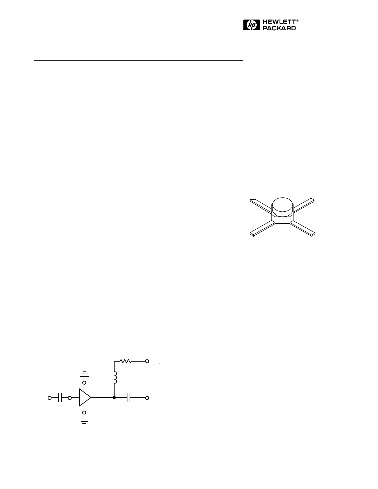
Typical Biasing Configuration
R
bias
35 micro-X Package
,
MAX
Note:
1. Short leaded 36 package available
upon request.
V
> 7 V
CC
[1]
RFC (Optional)
C
block
IN OUT
4
3
MSA
1
2
C
block
= 5 V
V
d
5965-9697E
6-274
Page 2
MSA-0235, -0236 Absolute Maximum Ratings
Parameter Absolute Maximum
Device Current 60 mA
Power Dissipation
RF Input Power +13 dBm
Junction Temperature 200°C
Storage Temperature
Notes:
1. Permanent damage may occur if any of these limits are exceeded.
2. T
3. Derate at 6.9 mW/° C for T
4. Storage above +150°C may tarnish the leads of this package making it
5. The small spot size of this technique results in a higher, though more
= 25°C.
CASE
difficult to solder into a circuit.
accurate determination of θ
MENTS section “Thermal Resistance” for more information.
[2,3]
[4]
C
325 mW
–65 to 200° C
> 153° C.
than do alternate methods. See MEASURE-
jc
[1]
Thermal Resistance
θjc = 145°C/W
[2,5]
:
Electrical Specifications
Symbol Parameters and Test Conditions: Id = 25 mA, Z
G
P
∆G
f
3 dB
VSWR
Power Gain (|S21|2) f = 0.1 GHz dB 11.5 12.5 13.5
Gain Flatness f = 0.1 to 1.6 GHz dB ±0.6 ± 1.0
P
3 dB Bandwidth GHz 2.7
Input VSWR f = 0.1 to 3.0 GHz 1.2:1
[1]
, T
A
= 25° C
= 50 Ω Units Min. Typ. Max.
O
Output VSWR f = 0.1 to 3.0 GHz 1.4:1
NF 50 Ω Noise Figure f = 1.0 GHz dB 6.5
P
IP
t
V
1 dB
3
D
d
Output Power at 1 dB Gain Compression f = 1.0 GHz dBm 4.5
Third Order Intercept Point f = 1.0 GHz dBm 17.0
Group Delay f = 1.0 GHz psec 125
Device Voltage V 4.5 5.0 5.5
dV/dT Device Voltage Temperature Coefficient mV/°C –8.0
Note:
1. The recommended operating current range for this device is 18 to 40 mA. Typical performance as a function of current
is on the following page.
Part Number Ordering Information
Part Number No. of Devices Container
MSA-0235 10 Strip
MSA-0236-BLK 100 Antistatic Bag
MSA-0236-TR1 1000 7" Reel
For more information refer to PACKAGING section, “Tape and Reel
Packaging for Semiconductor Devices.”
6-275
Page 3

MSA-0235, -0236 Typical Scattering Parameters (Z
Freq.
S
11
S
21
= 50 Ω, TA = 25° C, I
O
S
12
S
= 25 mA)
d
GHz Mag Ang dB Mag Ang dB Mag Ang Mag Ang
0.1 .08 170 12.6 4.25 176 –18.6 .118 2 .16 –6
0.2 .08 163 12.5 4.23 171 –18.5 .119 2 .15 –10
0.4 .08 147 12.5 4.19 161 –18.4 .120 4 .15 –21
0.6 .08 130 12.4 4.14 152 –18.3 .121 4 .15 –30
0.8 .07 112 12.2 4.09 143 –18.1 .125 7 .15 –39
1.0 .07 91 12.1 4.02 134 –18.0 .126 10 .15 –46
1.5 .06 47 11.6 3.80 112 –17.3 .137 11 .13 –66
2.0 .03 –1 11.0 3.53 91 –16.3 .153 10 .11 –89
2.5 .03 –115 10.2 3.24 75 –15.4 .169 12 .09 –111
3.0 .09 –157 9.3 2.92 57 –15.1 .176 8 .08 –127
3.5 .16 –175 8.3 2.60 39 –14.4 .190 3 .09 –129
4.0 .20 173 7.2 2.29 23 –14.1 .198 –2 .11 –118
5.0 .27 136 5.2 1.81 –6 –13.5 .211 –11 .15 –117
6.0 .41 94 3.2 1.44 –33 –13.5 .212 –24 .11 –148
A model for this device is available in the DEVICE MODELS section.
22
Typical Performance, T
(unless otherwise noted)
14
12
Gain Flat to DC
10
8
(dB)
p
G
6
4
2
0
0.1 0.3 0.5 1.0 3.0 6.0
FREQUENCY (GHz)
Figure 1. Typical Power Gain vs.
Frequency, TA = 25°C, Id = 25 mA.
13
12
(dB)
p
G
11
8
7
6
5
4
(dBm)
1 dB
3
P
2
–55 –25 +25 +85 +125
TEMPERATURE (°C)
Figure 4. Output Power at 1 dB Gain
Compression, NF and Power Gain vs.
Mounting Surface Temperature,
f=1.0 GHz, Id = 25 mA.
G
P
NF
P
1 dB
= 25° C
A
8
7
6
5
NF (dB)
4
3
2
40
TC = +125°C
TC = +25°C
30
TC = –55°C
20
(mA)
d
I
10
0
0 234561
Vd (V)
Figure 2. Device Current vs. Voltage.
12
Id = 40 mA
10
8
(dBm)
6
1 dB
P
4
Id = 25 mA
2
Id = 18 mA
0
0.1 0.2 0.3 0.5 2.01.0 4.0 0.1 0.2 0.3 0.5 2.01.0 4.0
FREQUENCY (GHz)
Figure 5. Output Power at 1 dB Gain
14
12
10
(dB)
p
G
8
Id (mA)
0.1 GHz
0.5 GHz
1.0 GHz
2.0 GHz
6
4
15 25 30 403520
Figure 3. Power Gain vs. Current.
7.5
7.0
6.5
NF (dB)
6.0
5.5
Id = 18 mA
Id = 25 mA
Id = 40 mA
FREQUENCY (GHz)
Figure 6. Noise Figure vs. Frequency.
Compression vs. Frequency.
6-276
Page 4

35 micro-X Package Dimensions
4
GROUND
RF OUTPUT
AND BIAS
A02
2
GROUND
Notes:
(unless otherwise specified)
1. Dimensions are
.100
2.54
2. Tolerances
in .xxx = ± 0.005
mm .xx = ± 0.13
.057 ± .010
1.45 ± .25
.085
2.15
RF INPUT
13
.020
.508
.083
2.11
in
mm
DIA.
.022
.56
.455 ± .030
11.54 ± .75
.006 ± .002
.15 ± .05
6-277
 Loading...