

Page 1
EEPROMs
MN61113, MN61113S
2K-Bit EEPROMs
Overview
The MN61113 and MN61113S are 2048-bit, bit sequential EEPROMs with built-in address counters. They sequentially increment the address with the clock input to
produce serial output.
They include built-in charge pump circuit and timer for
automatically erasing, writing, and modifying data using
only a single 3 volt power supply.
To reduce write times, they include a block write function for writing up to 32 bits at a time. This function makes
it possible to rewrite the contents of all 2048 bits within
1 second (typ.).
Features
2048 words × 1 bit organization
Built-in reset function
Tristate output
Low power consumption
• 3 volt read: 1.5 mW (max.)
• 3 volt program: 6 mW (max.)
• 3 volt standby: 60 µW (max.)
Single 3 volt power supply (charge pump circuit
built in)
Self timer for use in automatically erasing and
writing data
Built-in data polling function
Write cycles: 105 times
Data storage interval: 10 years
Pull-up resistor on CE pin.
Pull-down resistors on PGM, CLK, and RST pins
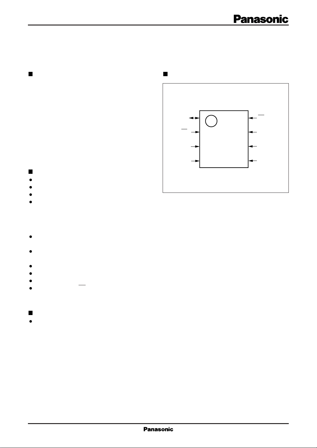
Pin Assignment
MN61113 DIP008-P-0300A
MN61113S SOP008-P-0225
CC
1
2
3
4
(TOP VIEW)
DATA
CE
V
GND
8
OE
7
RST
6
CLK
5
PGM
Applications
Personal wireless equipment, cordless telephones,
storage for recognition and adjustment data for
terminals, etc.
1
Page 2
MN61113, MN61113S EEPROMs
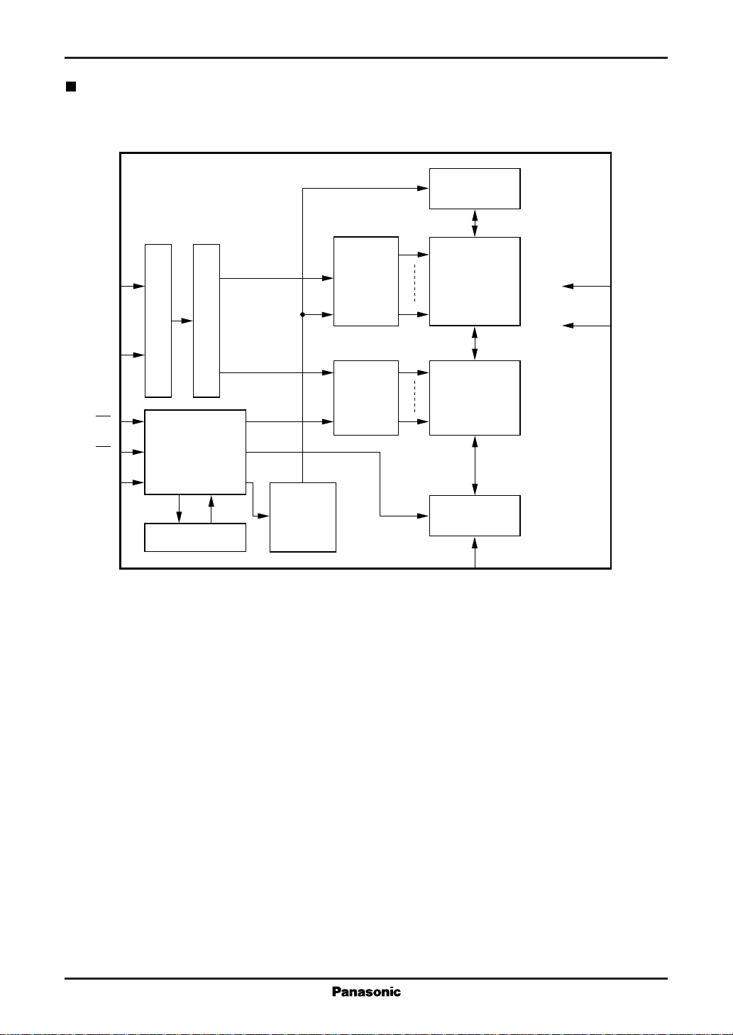
Block Diagram
Data latch pump
CLK
RST
6
7
Clock generator
8-bit counter
Row decoder
64 × 16
cell matrix
3
V
CC
4
GND
CE
OE
PGM
2
8
5
Control logic
Timer
VPP generator
Column
decoder
Column gate
Data I/O buffer
1
DATA
2
Page 3

EEPROMs MN61113, MN61113S
Pin Descriptions
Pin No. Symbol Pin Name
1 DATA Data I/O
2 CE Chip enable
3VCCPower supply voltage
4 GND Ground
5 PGM Program
6 CLK Clock input
7 RST Reset input
8 OE Output enable
Electrical Characteristics
VCC=2.6 to 3.5V, Ta=–10˚C to +60˚C
3 Volt Operation
Parameter Symbol Test Conditions
Power supply voltage V
"L" level input leakage current I
"H" level input leakage current I
Output leakage current I
Read mode 2.6 3.5
CC
Program mode 3.0 3.5
CE pin –50 —
LIL
Other pins –10 10
PGM, CLK, and RST pins — –20
LIH
Other pins –10 10
LO
min max
—10 µA
Unit
V
µA
µA
"L" level input voltage V
"H" level input voltage V
power supply current I
V
CC
(during operation) CLK;f=250kHz µA
IL
IH
CC
Read mode
– 0.1
0.8 V
V
CC
— 500
0.2
V
CC
CC
+0.3
V
V
Program mode — 2000
power supply current I
V
CC
(during standby) RST and PGM pins at VCC; µA
CE = VCC+ 0.3 V;
SB
—20
CLK pin open
"L" level output voltage V
"H" level output voltage V
OL
IOL=400µA — 0.3 V
OH
IOH=10µA
V
CC
– 0.3
—V
3
Page 4

MN61113, MN61113S EEPROMs
Function Descriptions
Operating Modes
Pin Symbol
Operating Mode
(Pin No.)
Read V
Standby V
Program V
CE OE PGM DATA
(2) (8) (5) (1)
IL
IH
IL
V
IL
××High-impedance
V
IH
× D
D
OUT
IN
4
Page 5

EEPROMs MN61113, MN61113S
Package Dimensions (Unit:mm)
MN61113 DIP008-P-0300A
–0.05
+0.20
85
6.40±0.20
14
9.60±0.40
3.30±0.20
4.80 max.
0.25
0° to 15°
7.62±0.20
3.45±0.30
MN61113S SOP008-P-0225
85
4.30±0.20
6.50±0.30
0.60
2.54
0.50±0.10
0.70±0.10
1.30±0.10
0.70 min.
SEATING PLANE
14
5.00±0.20
1.50±0.20
DETAIL F
1.90
1.10±0.20
SEATING PLANE SEE DETAIL F
1.27
0.40±0.10
SEATING PLANE
0.30
5
Page 6

 Loading...