

Page 1

MITSUMI
AV Switch for I2C BUS Control, 4-input, 3-output and Canal Plus Compatible MM1422, 1423, 1442, 1443
AV Switch for I2C BUS Control, 4-input, 3-output
and Canal Plus Compatible
Monolithic IC MM1422, 1423, 1442, 1443
Outline
These ICs are four-input, three-output AV switches under I2C BUS control with Canal Plus support, intended
for use in VCRs and DVD for the European market. There are four models, described below. Audio
subsystems are either stereo or monaural; video subsystems either do or do not have a clamping circuit.
Features
1. I2C BUS serial control.
2. Internal two-output 75Ωvideo driver, internal two-output 600Ω audio driver.
3. Audio mute function through an external pin.
4. Operating power supply voltage 11 to 13 V
5. Models both with and without video subsystem clamp.
6. Models with monaural and stereo audio subsystems.
Package
SSOP-34A (MM1443XJ)
SDIP-32A (MM1443XD)
Applications
(1)VCRs with Canal Plus Support for the European Market.
(2)DVD
Series Table
Video input
Stereo Monaural
Package
clamp
SDIP-32A SSOP-34A
MM1422
MM1423
MM1442
MM1443
Page 2
MITSUMI
AV Switch for I2C BUS Control, 4-input, 3-output and Canal Plus Compatible MM1422, 1423, 1442, 1443
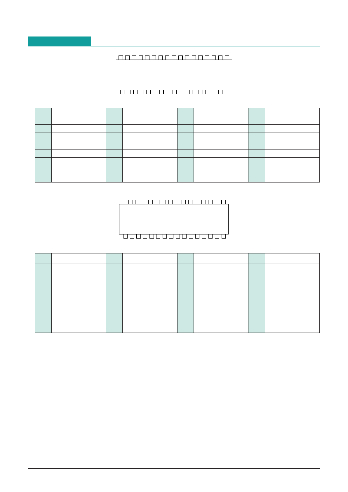
SDIP-32A
13 6
10
24587129
11 16151413
32 24 2127 25 23 22 2026 173031 29 28 1819
1 E1-V 9 Mute 17 GND1 25 LOUT1
2 V
CC2 10 E1
-
L 18 TUN-R(N.C.) 26 TUN-V
3 E2
-
V 11 FS 19 ROUT3(N.C.) 27 VOUT3
4 V
CC1 12 EXT
-
R(N.C.) 20 ROUT2(N.C.) 28 VOUT2
5 EXT
-
V 13 Port1 21 ROUT1(N.C.) 29 VOUT1
6 EXT
-
L 14 E2-R(N.C.) 22 TUN-L 30 SDA
7 BIAS 15 Port2 23 L
OUT3 31 SCL
8 E2
-
L 16 E1-R(N.C.) 24 LOUT2 32 GND2
Pin Assignment
SSOP-34A
13 6
10
24587129
11 16151413
323334 24 2127 25 23 22 2026
17
3031 29 28 1819
1 E1-V 10 E1-L 19 GND1 28 TUN-V
2 V
CC2 11 FS 20 TUN
-
R(N.C.) 29 VOUT3
3 E2
-
V 12 EXT-R(N.C.) 21 ROUT3(N.C.) 30 VOUT2
4 V
CC1 13 Port1 22 ROUT2(N.C.) 31 VOUT1
5 EXT
-
V 14 E2-R(N.C.) 23 ROUT1(N.C.) 32 SDA
6 EXT
-
L 15 Port2 24 TUN-L 33 SCL
7 BIAS 16 E1
-
R(N.C.) 25 LOUT3 34 GND2
8 E2
-
L 17 NC 26 LOUT2
9 Mute 18 NC 27 L
OUT1
MM1443XJ
MM1443XD
Page 3
MITSUMI
AV Switch for I2C BUS Control, 4-input, 3-output and Canal Plus Compatible MM1422, 1423, 1442, 1443
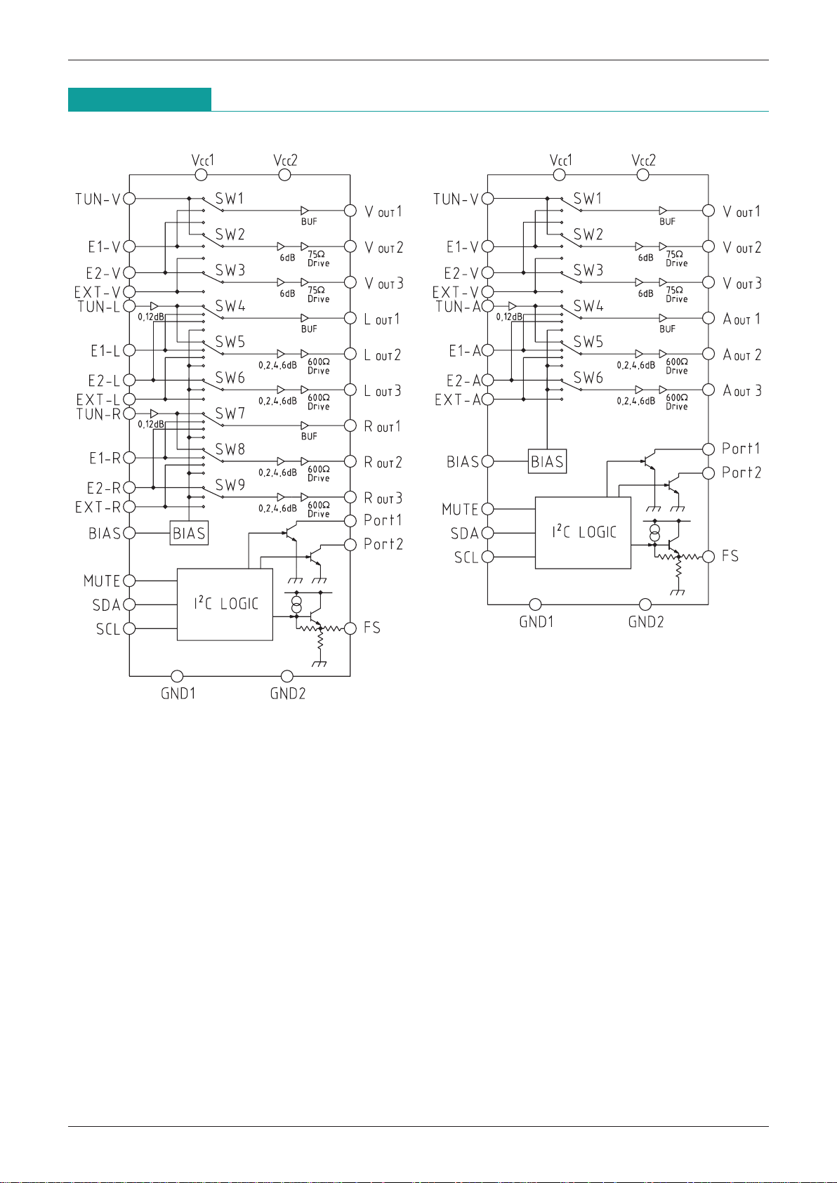
Block Diagram
Stereo type (MM1423, MM1443) Monaural type (MM1422, MM1442)
Page 4

MITSUMI
AV Switch for I2C BUS Control, 4-input, 3-output and Canal Plus Compatible MM1422, 1423, 1442, 1443
Pin No.
Pin name
Functions Equivalent circuit diagram
1 E1
-
V Video input pin
3 E2
-
V
5
EXT-V
28
TUN-V
2 VCC2VCC2 is power supply voltage pin for
4 V
CC175Ω driver
13 Port1 Port output pin
15 Port2
6
EXT-L
Audio input pin
8 E2
-
L
10 E1
-
L
12
EXT-R
14 E2-R
16 E1
-
R
20
TUN-R
24
TUN-L
7 BIAS Bias pin
Pin Description
AV Switch for I2C BUS Control, 4-input, 3-output
and Canal Plus Compatible
Monolithic IC MM1443
Introduction of Main Model
Page 5

MITSUMI
AV Switch for I2C BUS Control, 4-input, 3-output and Canal Plus Compatible MM1422, 1423, 1442, 1443
Pin No.
Pin name
Functions Equivalent circuit diagram
9 Mute Mute pin
19 GND1 GND2 is a GND pin for 75Ω driver
34 GND2
11 FS FS output pin
21 R
OUT3 Audio driver output pin
22 R
OUT2
25 L
OUT3
26 L
OUT2
23 R
OUT1 Audio buffer output pin
27 L
OUT1
Page 6

MITSUMI
AV Switch for I2C BUS Control, 4-input, 3-output and Canal Plus Compatible MM1422, 1423, 1442, 1443
Pin No.
Pin name
Functions Equivalent circuit diagram
29 V
OUT3 Video driver output pin
30 V
OUT2
31 V
OUT1 Video buffer output pin
32 SDA SDA pin
33 SCL SCL pin
17 NC
18
Page 7

MITSUMI
AV Switch for I2C BUS Control, 4-input, 3-output and Canal Plus Compatible MM1422, 1423, 1442, 1443
Absolute Maximum Ratings
(Ta=25°C)
Recommend Operating Conditions
Electrical Characteristics
(Except where noted otherwise, Ta=25°C, VCC=12V)
Item Symbol Ratings Unit
Storage temperature T
STG
-
40~+125 °C
Operating temperature T
OPR -25~+75 °C
Power supply voltage V
CC max. 15 V
Allowable loss Pd 700 mW
Item Symbol Ratings Unit
Operating temperature T
OPR -25~+75 °C
Operating voltage V
OP 11~13 V
Item Symbol Measurement conditions Min. Typ. Max. Unit
Consumption current I
CC No-signal, no-load 33.5 40.0 mA
[FS pin output level]
High voltage V
FSH FS pin control High selected 9.5 11.0 12.0 V
Middle voltage V
FSM FS pin control Mid selected 4.5 6.0 7.0 V
Low voltage V
FSL FS pin control Low selected 0.2 1.0 V
[Crosstalk]
V
OUT1 CTV1
VOUT2 CTV2 VIN=1VP
-
P f=4.43MHz
-
70-50 dB
V
OUT3 CTV3
LOUT1 CTL1
LOUT2 CTL2 VIN=1Vrms f=1kHz
-
90-70 dB
L
OUT3 CTL3
ROUT1 CTR1
ROUT2 CTR2 VIN=1Vrms f=1kHz
-
90-70 dB
R
OUT3 CTR3
[VOUT1]
Voltage gain G
V1 VIN=1VP-P f=100kHz
-
0.5 0 +0.5 dB
Frequency characteristic F
V1 VIN=1VP-P 10MHz/100kHz
-
1.0 0 +1.0 dB
Differential gain DG
1 VIN=1VP-P: staircase APL = 10~90%
-
3 0 +3 %
Differential phase DP
1 VIN=1VP-P: staircase APL = 10~90%
-
3 0 +3 deg
Maximam output level V
OV1
f = 100kHz, Maximum output at THD < 1.0%
2.1 VP
-
P
Input pin voltage VIV1 No-signal, no-load 2.3 2.8 3.3 V
Output pin voltage V
OV1 No-signal, no-load 1.0 1.5 2.0 V
[V
OUT2, VOUT3]
Voltage gain
G
V2
VIN=1VP
-
P f=100kHz 5.5 6.0 6.5 dB
G
V3
Frequency characteristic
F
V2
VIN=1VP
-
P 10MHz/100kHz
-
1.0 0 +1.0 dB
F
V3
Differential gain
DG
2
VIN=1VP
-
P: staircase APL = 10~ 90%
-
3 0 +3 %
DG
3
Page 8

MITSUMI
AV Switch for I2C BUS Control, 4-input, 3-output and Canal Plus Compatible MM1422, 1423, 1442, 1443
Item Symbol Measurement conditions Min. Typ. Max. Unit
Differential phase
DP
2
VIN=1VP
-
P: staircase APL = 10~90%
-
3 0 +3 deg
DP
3
Maximam output level
V
OV2
f = 100kHz, Maximum output at THD < 1.0%
4.2 VP
-
P
VOV3
Input pin voltage
V
IV2
No-signal, no-load 2.3 2.8 3.3 V
V
IV3
Output pin voltage
V
OV2
No-signal, no-load 1.0 1.5 2.0 V
V
OV3
[LOUT1, ROUT1]
G
1L1
VIN=1Vrms f=1kHz
-
0.5 0 +0.5 dB
Voltage gain
TUN-L GAIN adjustment at 0dB
G
2L1
VIN=0.25Vrms f=1kHz
11.5 12 12.5 dB
TUN-L GAIN adjustment at 12dB
Maximam output level D
L1
VCC= 12V, f = 1kHz Maximum output at THD < 0.5%
3.0 Vrms
Total harmonic distortion THD
L1 VIN such that VOUT = 1Vrms, f = 1kHz 0.03 0.1 %
Output noise voltage V
NL1 A curve band 20kHz 3 50
µVrms
Output offset voltage VOFL1 DC step for switching
-
15 0 15 mV
Input impedance Z
INL1 100 150 200 kΩ
Input pin voltage V
IL1 No-signal, no-load 5.30 5.65 6.00 V
Output pin voltage V
OL1 No-signal, no-load 5.30 5.65 6.00 V
[L
OUT2, LOUT3, ROUT2, ROUT3]
G
OL2 VIN=1Vrms TUN
-
L=0dB
-
0.5 0 +0.5 dB
G
OL3 Output GAIN adjustment at 0dB
G
2L2 VIN=1Vrms TUN
-
L=0dB
1.5 2 2.5 dB
Voltage gain
G
2L3 Output GAIN adjustment at 2dB
G
4L2 VIN=1Vrms TUN
-
L=0dB
3.5 4 4.5 dB
G
4L3 Output GAIN adjustment at 4dB
G
6L2 VIN=1Vrms TUN
-
L=0dB
5.5 6 6.5 dB
G
6L3 Output GAIN adjustment at 6dB
Maximam output level
V
L2 VCC=12V f=1kHz
3.0 Vrms
V
L3 Maximum output when THD < 0.5%
Total harmonic distortion
THD
L2 VIN such that VOUT = 1Vrms
0.03 0.1 %
THD
L3 f=1kHz G=0, 2, 4, 6dB
Output noise voltage
V
NL2
A curve band 20kHz 20 50
µVrms
VNL3
Output offset voltage
V
OFL2
DC step for switching
-
15 0 15 mV
V
OFL3
Input impedance
Z
INL2
100 150 200 kΩ
Z
INL3
Input terminal voltage
V
IL2
No-signal, no-load 5.30 5.65 6.00 V
V
IL3
Output terminal voltage
V
OL2
No-signal, no-load 5.30 5.65 6.00 V
V
OL3
[Logic] (refer to next page)
Input voltage L V
IL I
2
C logic L level judgment value 0.0 1.5 V
Input voltage H V
IH I
2
C logic H level judgment value 3.0 5.0 V
Low level output voltage V
OL for SDA 3mA inflow 0.0 0.4 V
High level input current I
IH for SDA, SCL = 4.5V impressed
-
10 +10 µA
Low level input current I
IL for SDA, SCL = 0.4V impressed
-
10 +10 µA
Clock frequency f
SCL 100 kHz
Page 9

MITSUMI
AV Switch for I2C BUS Control, 4-input, 3-output and Canal Plus Compatible MM1422, 1423, 1442, 1443
Item Symbol Measurement conditions Min. Typ. Max. Unit
Data transfer waiting time t
BUF 4.7 µS
SCL start hold time t
HD : STA 4.0 µS
SCL low level hold time t
LOW 4.7 µS
SCL high level hold time t
HIGH 4.0 µS
SCL start setup time t
SU : STA 4.7 µS
SDA data hold time t
HD : DAT 200 nS
SDA data setup time t
SU : DAT 250 nS
SCL rise time t
R 1000 nS
SCL fall time t
F 300 nS
SCL stop setup time t
SU : STO 4.0 µS
SDA
SCL
P S Sr P
t
BUF
t HD:STA t HD:DAT t SU:DAT t SU:STA t SU:STOt HIGHt LOW
t R t F
I2C BUS control signal
I2C BUS
SDA
SCL
S 12345678A12378A P
S : Start Condition
P : Stop Condition
A : Acknowledge
I2C BUS (Inter IC BUS) is an inter bus system developed by Philips Co. It transmits and receives data through
2 (SDA, SCL) lines. Data are transmitted and received in the units of bytes by MSB first from the start
condition.
[Control registers]
Control registers are data sent from the master for determining the switch condition of the MM1422 series.
AA PAS
Address byte Control data
Slave address
R/W
10010000
Control Register 1
b7 b6 b5 b4 b3 b2 b1 b0
Control Register 2
b7 b6 b5 b4 b3 b2 b1 b0
Page 10

MITSUMI
AV Switch for I2C BUS Control, 4-input, 3-output and Canal Plus Compatible MM1422, 1423, 1442, 1443
The data format of the MM1422 series is set as shown in the above figure. Out of the address bytes, first 7
bits are assigned to the slave addresses, while the residual 1 bit is assigned to the R/W bit. Set the R/W bit to
0 when data are used as control registers. Slave address of the MM1422 series is 90H. Each bit of control
registers is reset to 0. MM1422 series consists of one address byte and two control data bytes(3 bytes in
total). For details of the control contents of control register 1 and 2, refer to the separate table.
All data over the limited length (4th and subsequent bytes) are fully neglected. Because of this, the faulty
operation that switch changes by the data after the 4th byte doesn't occur.
Each audio output can be set to mute by setting MUTE terminal to high.
[Status registers]
There is no preparation of the status register in MM1422 series. A status register returns all the 1 when is set
in the R/W bit.
b7 b6 b5 b4 b3 b2 b1 b0
OUT 1 select OUT 2 select OUT 3 select FS CTRL
b7 b6 b5 b4 b3 b2 b1 b0
0, 12dB select
Port 1 CTRL Port 2 CTRL
Audio OUT2 gain select Audio OUT3 gain select Mute
[Control Register 1]
[Control Register 2]
S
Slave address R/W
A
status register
NA P
10010001 b7b6b5b4b3b2b1b0
Address byte Status data
Page 11

MITSUMI
AV Switch for I2C BUS Control, 4-input, 3-output and Canal Plus Compatible MM1422, 1423, 1442, 1443
Switch Control Table
[Control register 1] (2nd byte)
[Control register 2] (3rd byte)
b7 b6 b5 b4 b3 b2 b1 b0 V OUT1 A OUT1 V OUT2 A OUT2 V OUT3 A OUT3 FS
00
*
1 MUTE
0 1 TUNER TUNER
10
SCART E1 SCART E1
11
SCART E2 SCART E2
00
*
1 MUTE
0 1 TUNER TUNER
10
SCART E1 SCART E1
1 1 EXT IN EXT IN
00
*
2 MUTE
0 1 EXT IN EXT IN
10
SCART E2 SCART E2
11
SCART E2 SCART E2
0 0 Low
0 1 Middle
1 0 High
1 1 High
Note 1 : Previous choice condition is held. TUNER is chosen at power on.
Note 2 : Previous choice condition is held. EXT IN is chosen at power on.
b7 b6 b5 b4 b3 b2 b1 b0 0, 12dB Port 1 Port 2
GainOUT2 GainOUT3
MUTE
0 0dB
1 12dB
0 Low
1 High
0 Low
1 High
0 0 0dB
0 1 2dB
1 0 4dB
1 1 6dB
0 0 0dB
0 1 2dB
1 0 4dB
1 1 6dB
0 OFF
1ON
Page 12

MITSUMI
AV Switch for I2C BUS Control, 4-input, 3-output and Canal Plus Compatible MM1422, 1423, 1442, 1443
Measuring Circuit
Page 13

MITSUMI
AV Switch for I2C BUS Control, 4-input, 3-output and Canal Plus Compatible MM1422, 1423, 1442, 1443
Application Circuit
 Loading...