

Page 1

MITSUMI
RGB Video Amplifier for Monitors MM1375
RGB Video Amplifier for Monitors
Monolithic IC MM1375
Outline
This IC is a wideband RGB video amplifier with DC control, developed for use in monitors. It has a differential
input comparator for brightness adjustment, and three matched DC control attenuators for contrast
adjustment. All DC control input is high impedance, and the operating range is set for easy interface with
serial bus control systems, at 0~4V. Also, the building-in blanking circuit clamps video output to less than
0.2V during blanking, enabling blanking on the CRT cathode.
Features
1. Low power consumption (VCC=8V, ICC=68mA)
2. Smaller capacity for clamping capacitor (0.1µF)
3. High band video amp 100MHZ @
4. Matched (±0.1dB) contrast adjustment attenuators built in
5. Built-in cutoff and brightness adjustment input comparators using external gate control
6. Built-in high input impedance DC contrast control, 0~4V
7. Output blanking function
8. Output can drive hybrid or discrete CRT driver directly
-
3dB
Package
SDIP-22A
Applications
1. High resolution RGB CRT monitors
2. AGC amps for video
3. Gain and DC offset control high bandwidth amps
4. Interface amps for LCD or CCD systems
Page 2

MITSUMI
Block Diagram
RGB Video Amplifier for Monitors MM1375
Page 3
MITSUMI
RGB Video Amplifier for Monitors MM1375
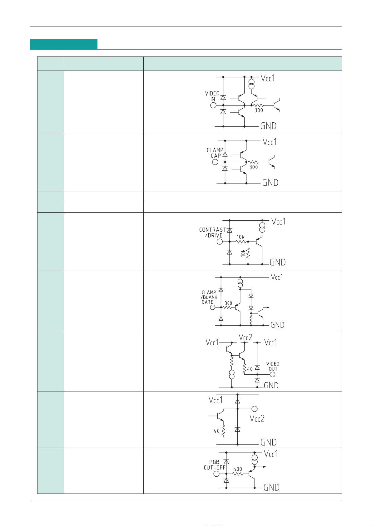
Pin Description
Pin no. Pin name Internal equivalent circuit diagram
1 R VIDEO IN
3 G VIDEO IN
6 B VIDEO IN
2 R CLAMP CAP
5 G CLAMP CAP
7 B CLAMP CAP
8 VCC1
4, 18 GND
9 CONTRAST
22 R DRIVE
15 G DRIVE
12 B DRIVE
10 BLANK GATE
11 CLAMP GATE
20 R VIDEO OUT
17 G VIDEO OUT
14 B VIDEO OUT
19 VCC2
21 R CUT-OFF ADJ
16 G CUT
13 B CUT
-
OFF ADJ
-
OFF ADJ
Page 4
MITSUMI
RGB Video Amplifier for Monitors MM1375
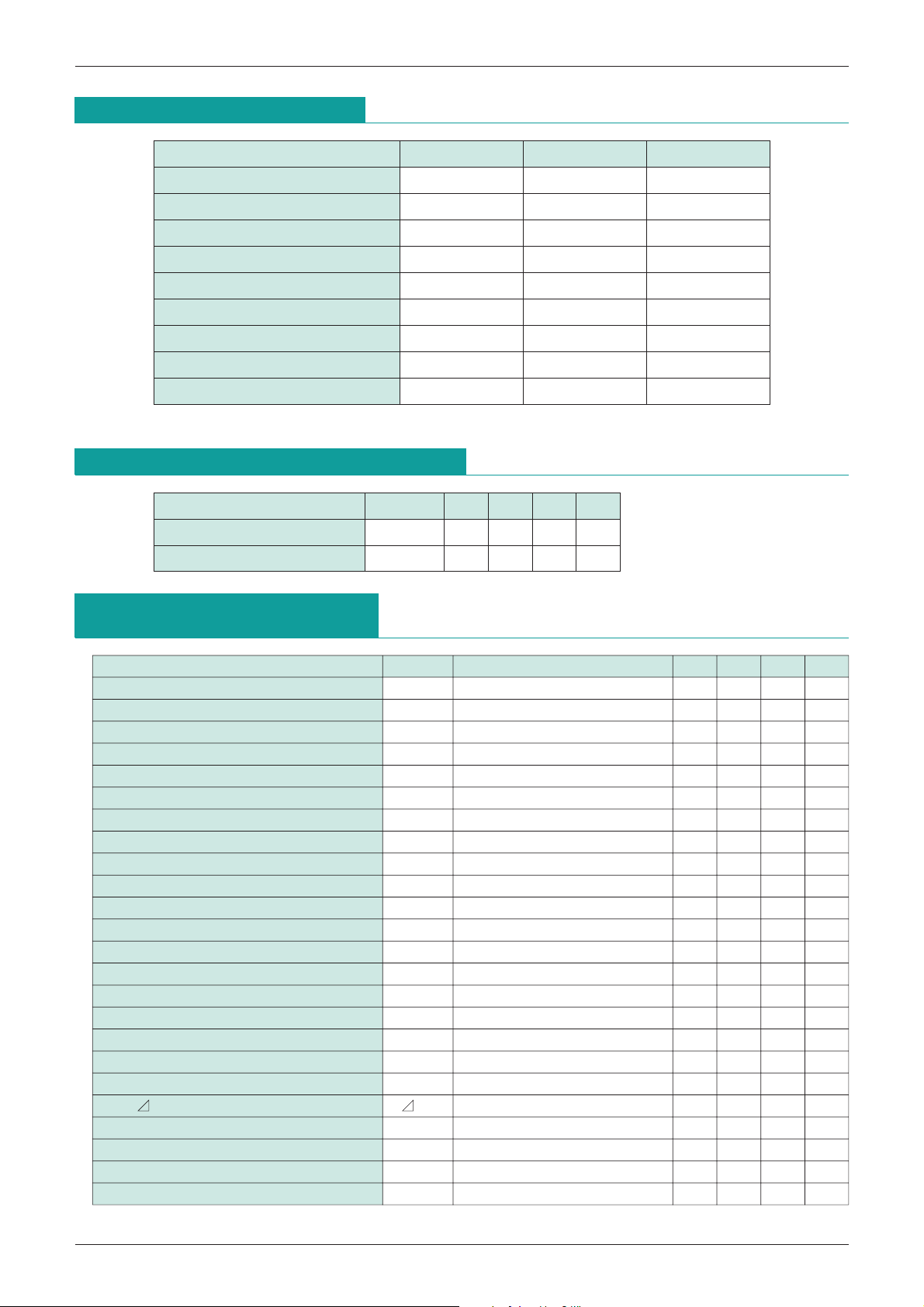
Absolute Maximum Ratings
(Ta=25°C)
Item Symbol Ratings Units
Storage temperature T
Operating temperature T
Power supply voltage 1 V
Power supply voltage 2 V
Input voltage range V
Video output current I
Allowable loss Pd 1.6 W
Electrostatic breakdown 2kV
Pin temperature 265
Note : Solder for 10S
Recommended Operating Conditions
Item Symbol Min. Typ. Max. Units
Operating power supply voltage 1
Operating power supply voltage 2
VCC1 7.6 8.0 8.4 V
VCC2 7.6 12.6 V
STG
OPR
CC110 V
CC215 V
IN
O 28 mA
-
40~+125 °C
-
20~+80 °C
<
<
GND
IN
CC
1
V
V
=
=
*
V
°C
(Ta=25°C)
DC Electrical Characteristics
Item Symbol Measurement conditions Min. Typ. Max. Units
Power supply current I
Video amp input voltage V
Video input resistance R
Clamp gate input voltage L V
Clamp gate input voltage H V
Clamp gate input current L I
Clamp gate input current H I
Input charging current I
Input discharge current I
Clamp cap charge current I
Clamp cap discharge current I
Clamp cap bias discharge current I
Blanking gate input voltage L V
Blanking gate input voltage H V
Blanking gate input current L I
Blanking gate input current H I
Video output voltage L V
Video output voltage H V
Black level output voltage V
Black level output voltage V
Output blanking voltage
Contrast control input current
Drive control input current I
Cutoff control input current
(Except where noted otherwise, Ta=25°C, VCC1=8V, VCC2=8~12V,
V9=4V, V10=4V, V11=0V, V
CC1VCC1+VCC26880mA
B 2.2 V
B 100 kΩ
CGL 0.8 1.2 V
CGH 1.6 2.0 V
CGL V11=0V
CGH V11=8V 0.01 1.0 µA
IN+ 0.75 1.0 mA
IN
- -
CL+ 0.75 1.0 mA
CL
- -
CLB 50 nA
BGL 0.8 1.2 V
BGH 1.6 2.0 V
BGL V10=0V
BGH V10=8V 0.01 1.0 µA
OL VC-O=0V 0.15 0.5 V
OH VC-O=6V 5.0 5.5 V
O VC-O=1V 1.0 V
O VC-O=1V ±100 mV
C-o=1.0V, V
DRV
=4V)
-
0.5-5.0 µA
0.75-1.0 mA
0.75-1.0 mA
-
1.0-5.0 µA
VOBLK V10=0V 100 300 mV
I9 V9=4V 190 µA
DBV VDBV=4V 190 µA
IC
-
O VC-O=0~4V
-
500 nA
Page 5
MITSUMI
RGB Video Amplifier for Monitors MM1375
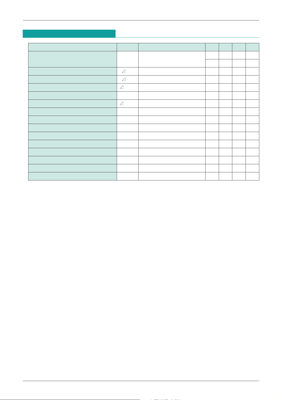
AC Electrical Characteristics
Item Symbol Measurement conditions Min. Typ. Max. Units
Video amp gain A
Gain attenuation 1 A
Gain attenuation 2 A
Drive control range A
Gain matching A
Gain change between amps A
Video amp distortion THD V
Video amp frequency bandwidth f
Output rise time tr V
Output fall time tf V
Video amp isolation 1 (f
Video amp isolation 2 (f
Blanking output fall time tr V
Blanking output fall time tf V
IN=10kHz) VSEP1 V9=4V
IN=10MHz) VSEP2 V9=4V
(Except where noted therwise, Ta=25°C, VCC1=8V, VCC2=8~12V)
V
V max.
V1VIN=635mVP-P, V9=2V
V2VIN=635mVP-P, V9=0.5V
VDRV VDRV=0~4V, V9=4V 6 dB
VMAT V9=VDRV=4V 0.3 dB
VMAT V9=4~2V 0.1 dB
BW VOUT=4VP-P, V9=VDRV=4V 100 MHz
IN=635mVP-P, V9=4V 5.4 7.0 V/V
V
DRV=4V 14.6 16.9 dB
-
6dB
-
38 dB
OUT=1VP-P 1%
OUT=4VP-P 3nS
OUT=4VP-P 4nS
-
70 dB
-
50 dB
OUT=1VP-P 7nS
OUT=1VP-P 7nS
Back-porch clamping pulse width tpw 200 nS
Page 6
MITSUMI
18
16
14
12
10
8
6
4
2
0
0.1 1 10 100 1000
Gain (dB)
Frequency (Hz)
tr=2.7nS
tr=4.3nS
X : 10nS/div
Y : 1v/div
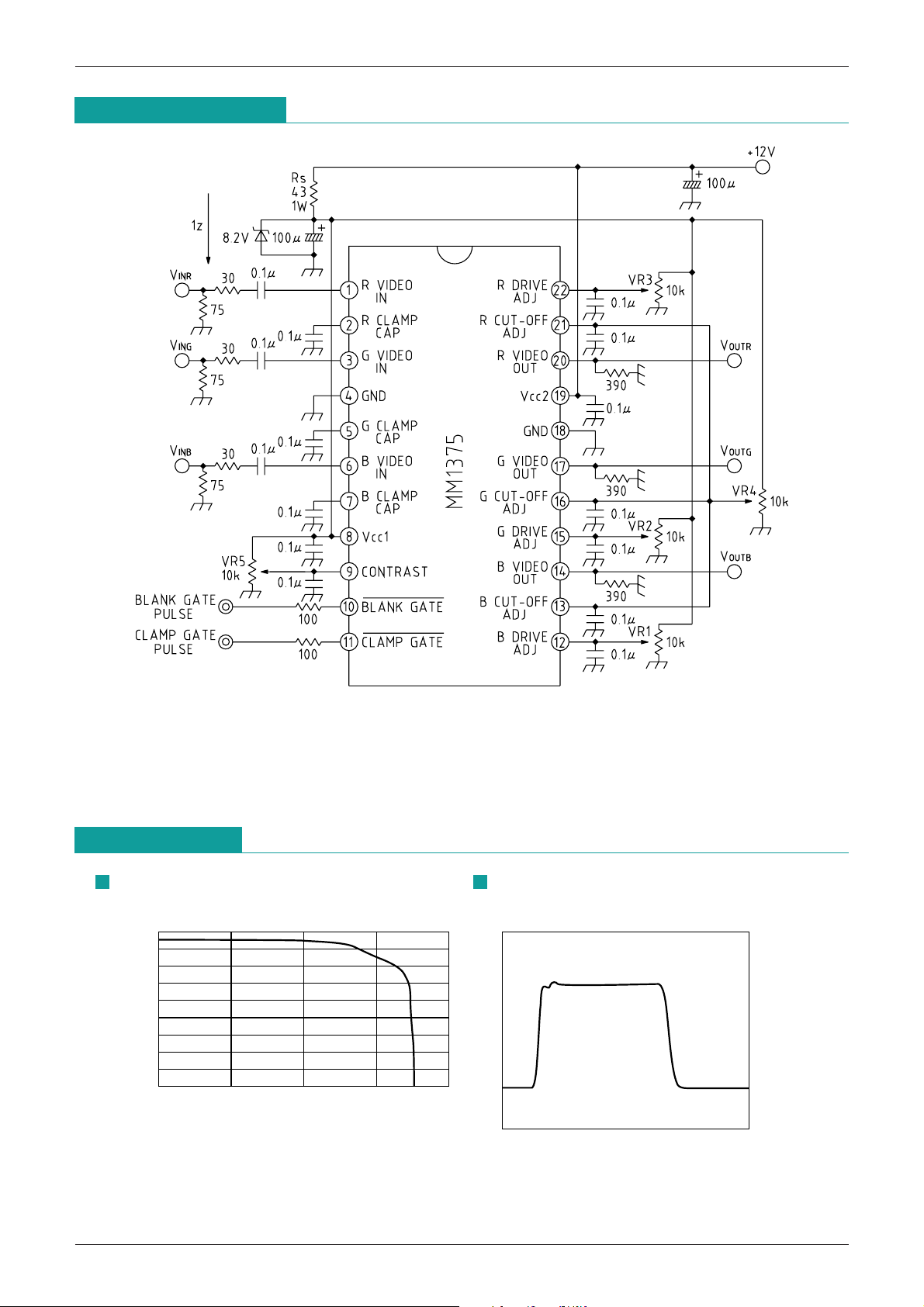
Application Circuits
RGB Video Amplifier for Monitors MM1375
Characteristics
Gain vs Frequency Pulse reaction
 Loading...