

Page 1

MITSUMI
MITSUMI
Protection of Lithium Ion Batteries MM1414
Protection of Lithium Ion Batteries
Monolithic IC MM1414
Outline
This IC is use to protect lithium-ion batteries consisting of three or four cells. It adopts a compact package
and has the functions of previous models, with functions for overcharge detection, overdischarge detection
and overcurrent detection. A dead time can be set externally.
Features
1. Overcharge detection voltage accuracy ±25mV/cell
2. Consumption current (Vcell=4.4V) 50µA typ.
3. Consumption current (Vcell=3.5V) 23µA typ.
4. Consumption current (Vcell=1.8V) 2µA typ.
5. Overcharge sensing dead time: can be set externally
6. PF detection: warning signal when cell voltage falls
Package
TSOP-20A
Applications
IC for protection of lithium-ion batteries consisting of three or four cells
Pin Assignment
1 OV 11 SEL
2 N.C 12 N.C
3 CS 13 CON
20 16 1319 17 15 14 1218 11
13 6824579
TSOP-20A
10
4 N.C 14 N.C
5 DCHG 15 V1
6 N.C 16 V2
7 CDC 17 V3
8 COL 18 V4
9 COV 19 N.C
10 GND 20 V
CC
Page 2
MITSUMI
MITSUMI
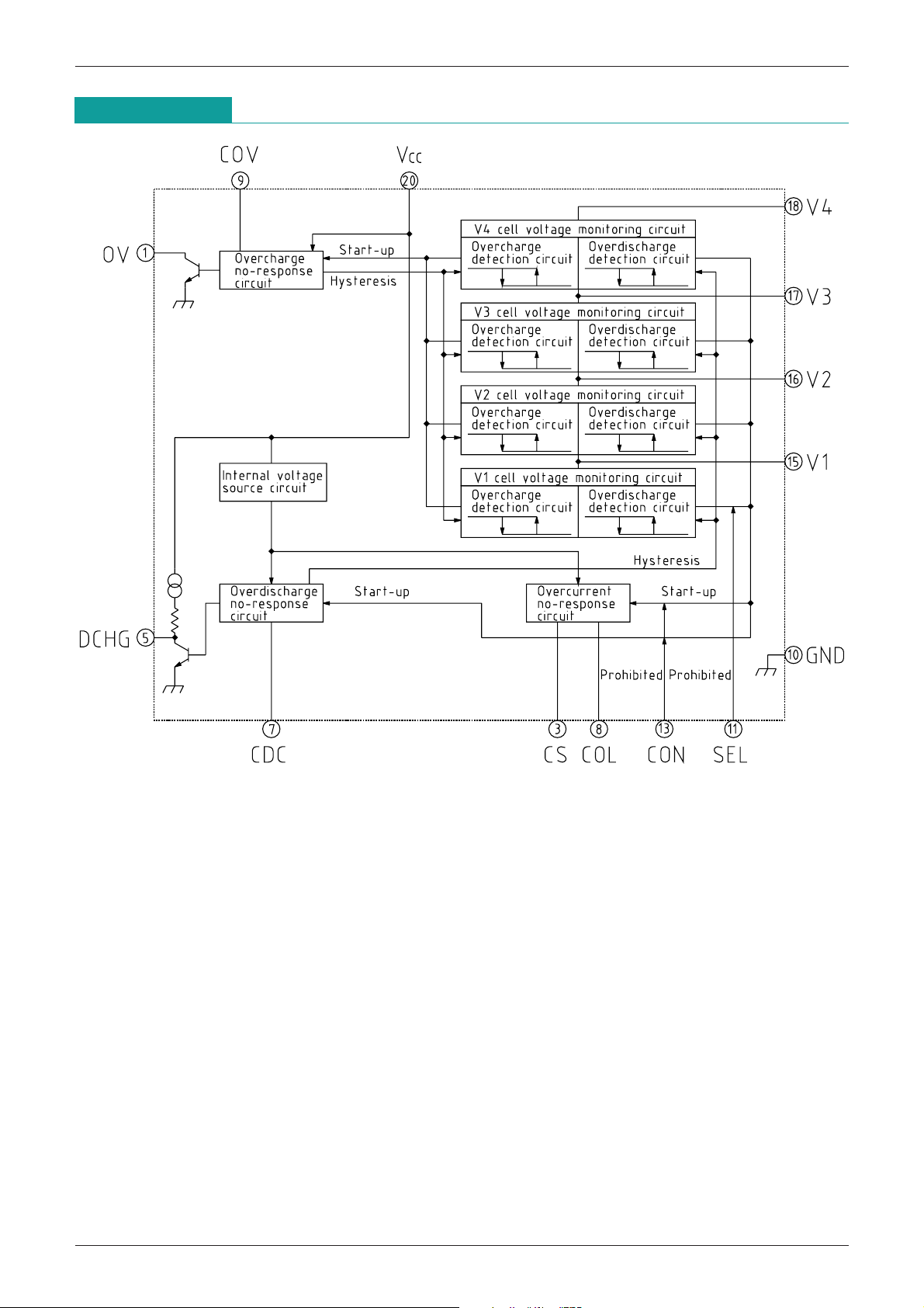
Block Diagram
Protection of Lithium Ion Batteries MM1414
Page 3
MITSUMI
Pin Description
Protection of Lithium Ion Batteries MM1414
Pin No.
Pin name
I/O Functions
Overcharge detection output pin
NPNTr open collector output
1 OV Output
Normal: high impedance
Overcharge: Low
2 N.C Not connected
Overcurrent detection pin
Monitors load current equivalently by the voltage drop between discharge control
FET source and drain, and makes DCHG pin high when the voltage goes below
3 CS Input
overcurrent detection voltage, turning off discharge control FET. After
overcurrent detection, current flows from this pin and when there is a light load,
overcurrent mode is released. This function does not operate in discharge mode.
4 N.C Not connected
Discharge control FET (P-ch) drive pin
5 DCHG Output Normal: Low
Overdischarge: High
6 N.C Not connected
Overdischarge detection dead time setting pin
7 CDC Input
Dead time can be set by connecting a capacitor between CDC pin and ground.
Overcurrent detection dead time setting pin
8 COL Input
Dead time can be set by connecting a capacitor between COL pin and ground.
9 COV Input
Overcharge detection dead time setting pin
Dead time can be set by connecting a capacitor between COV pin and ground.
10 GND Input Ground pin
3 cell switch pin SEL pin = GND: 3 cell (no V1 cell detection)
11 SEL Input
SEL pin = V
CC: 4 cell
12 N.C Not connected
Discharge FET ON/OFF pin
13 CON Input CON pin low; DCHG pin low
CON pin high; DCHG pin high
14 N.C Not connected
15 V1 Input V1 cell high side voltage input pin
16 V2 Input V2 cell high side voltage and V3 cell low side voltage input pin
17 V3 Input V3 cell high side voltage and V4 cell low side voltage input pin
18 V4 Input V4 cell high side voltage input pin
19 N.C Not connected
20 V
CC Input Power supply input pin
Page 4

MITSUMI
Pin Description
1 ; OV
3 ; CS
Protection of Lithium Ion Batteries MM1414
Equivalent circuit diagram Equivalent circuit diagram
9 ; COV
11 ; SEL
5 ; DCHG
7 ; CDC
13 ; CON
15 ; V1
8 ; COL
16 ; V2
Page 5

MITSUMI
Equivalent circuit diagram Equivalent circuit diagram
17 ; V3 18 ; V4
Protection of Lithium Ion Batteries MM1414
Absolute Maximum Ratings
(Ta=5°C)
Item Symbol Ratings Unit
Storage temperature T
Operating temperature T
Power supply voltage V
OV pin impressed voltage V
SEL pin impressed voltage V
CON pin impressed voltage V
CC max.
OV max.
SEL max.
CON max.
Allowable loss Pd 300 mW
Recommended Operating Conditions
Item Symbol Ratings Unit
Operating temperature T
Operating voltage V
STG
OPR
OPR
OPR +1.8~+24 V
-
40~+125 °C
-
20~+70 °C
-
0.3~24 V
-
0.3~24 V
-
0.3~24 V
-
0.3~24 V
-
20~+70 °C
Page 6

MITSUMI
MITSUMI
Protection of Lithium Ion Batteries MM1414
Electrical Characteristics
Item Symbol Measurement conditions Min. Typ. Max. Unit
Consumption current (VCCpin) 1
Consumption current (VCCpin) 2
Consumption current (VCCpin) 3
Consumption current (VCCpin) 4
Consumption current (VCCpin) 5
Consumption current (V4 pin) 1
Consumption current (V4 pin) 2
Consumption current (V4 pin) 3
V3 pin input current IV3 V
V2 pin input current IV2 V
V1 pin input current IV1 V
Overcharge detection voltage
Overcharge hysteresis voltage
Overcharge sensing dead time
VCELLUVCELL : 4.2V 4.4V
(Except where noted otherwise, Ta=25°C, VCC=V4+V3+V2+V1, V
CEL
=3.5V, CON=0V, SEL=0V)
ICC1VCELL=4.4V, CON=0V 55 110 µA
ICC2VCELL=3.5V, CON=0V 27 50 µA
ICC3VCELL=1.8V, CON=0V 2 4 µA
ICC4VCELL=3.5V, CON=VCC 12 20 µA
ICC5VCELL=1.8V, CON=VCC 12µA
I1V4 VCELL=4.4V 10 20 µA
I2V4 VCELL=3.5V 8 15 µA
I3V4 VCELL=1.8V 2.5 5.0 µA
CELL=3.5V ±300 nA
CELL=3.5V ±300 nA
CELL=3.5V ±300 nA
A, C 4.325 4.350 4.375
V
B, D 4.225 4.250 4.275
VU VCELL : 4.2V 4.4V 3.9V 140 200 260 mV
tOV COV=0.1µF 0.5 1.0 1.5 S
Overdischarge detection voltage
VCELLSVCELL : 3.5V 1.8V
C, D 2.20 2.30 2.40
A, B 1.90 2.00 2.10
Discharge resume voltage V
CELLDVCELL : 1.8V 3.5V 2.85 3.00 3.15 V
A, B 0.75 1.00 1.25
Overdischarge hysteresis voltage
VDS VCELLD-VCELLS
C, D 0.45 0.70 0.95
Overdischarge sensing dead time
Overcurrent detection voltage
Overcurrent hysteresis voltage
Overcurrent sensing dead time 1
Overcurrent sensing dead time 2
Overcurrent sensing dead time 3
Overcurrent reset conditions
tCDC CDC=0.1µF 0.5 1.0 1.5 S
VOC VCC-VCS, DCHG 135 150 165 mV
VOC 20 40 mV
tCOL1 COL=0.001µF 5 10 15 mS
tCOL2 COL=0.001µF, VCC-CS>1.0V 1.5 3.0 mS
tCOL3 COL=0.001µF 5 10 15 mS
Load release conditions 500kΩ
DCHG pin source current ISODCH VCELL=1.8V, SW1 : A VDCHG=VCC-0.8V 20 µA
DCHG pin sink current I
DCHG pin output voltage H V
DCHG pin output voltage L V
OV pin sink current I
OV pin leak current I
SIDCH VCELL=3.5V, SW1 : A VDCHG=0.8V 20 µA
THDCHVCC
THDCL VDCHG
SIOV VOV=0.4V, Ta=
LKOV VOV=24V 0.1 µA
-
VDCHG, ISO=20µA, SW1 : B 0.8 V
-
GND, ISI=-20µA, SW1 : B 0.8 V
-
20~+70°C 100 µA
V
V
CON pin L voltage DCHG= "High" 0.4 V
CON pin H voltage DCHG= "Low"
CON pin current V
CELL=3.5V, CON=0.4V 1 2 µA
VCC-
0.4
SEL pin L voltage for 3 cell 0.4 V
SEL pin H voltage for 4 cell
SEL pin current V
CELL=3.5V, SEL=0.4V 1 2 µA
VCC-
0.4
V
V
Page 7

MITSUMI
Overcharge detection voltage
Overcharge release voltage
Charge OFF
Sensing dead
Normal state Overcharge Normal state
Cell voltage
COV pin
OV pin (for pull up)
MITSUMI
Measuring Circuit
Protection of Lithium Ion Batteries MM1414
Timing Chart
For overcharge
Page 8

MITSUMI
Cell voltag
CON pin
CDC pin
DCHG pin
Overdischarge
detection voltage
Discharge OFF Charge start
Discharge resume voltage
Sensing
dead
Normal state Normal state Overdischarge Normal state
External control Normal state Normal state
Sensing dead Reset dead
Overcurrent Load release
Current flows
from CS pin
Normal state Overcurrent Normal state
CS pin
COL pin
DCHG pin
For overdischarge
Protection of Lithium Ion Batteries MM1414
For overcurrent
Page 9

MITSUMI
0.001
0.01
0.1
1
10
0.01 0.1 1
Pin capacitance (µF)
Dead time (S)
COL pin capacitance (pF)
100
10
1
100 1000 10000
Dead time (mS)
100 1000 10000
0
1
10
100
COL pin capacitance (pF)
Overcurrent Sensing
Dead Time 2 (mS)
Application Circuit
Protection of Lithium Ion Batteries MM1414
Characteristics
Overcharge & Overdischarge Sensing Dead Times
Overcurrent Sensing Dead Time 2
Overcurrent Sensing Dead Time 1,
Overcurrent Reset Dead Time
Note: The above characteristics are representative values only, and are not guaranteed.
 Loading...