

Page 1
MITSUMI
Audio MM1407
Audio
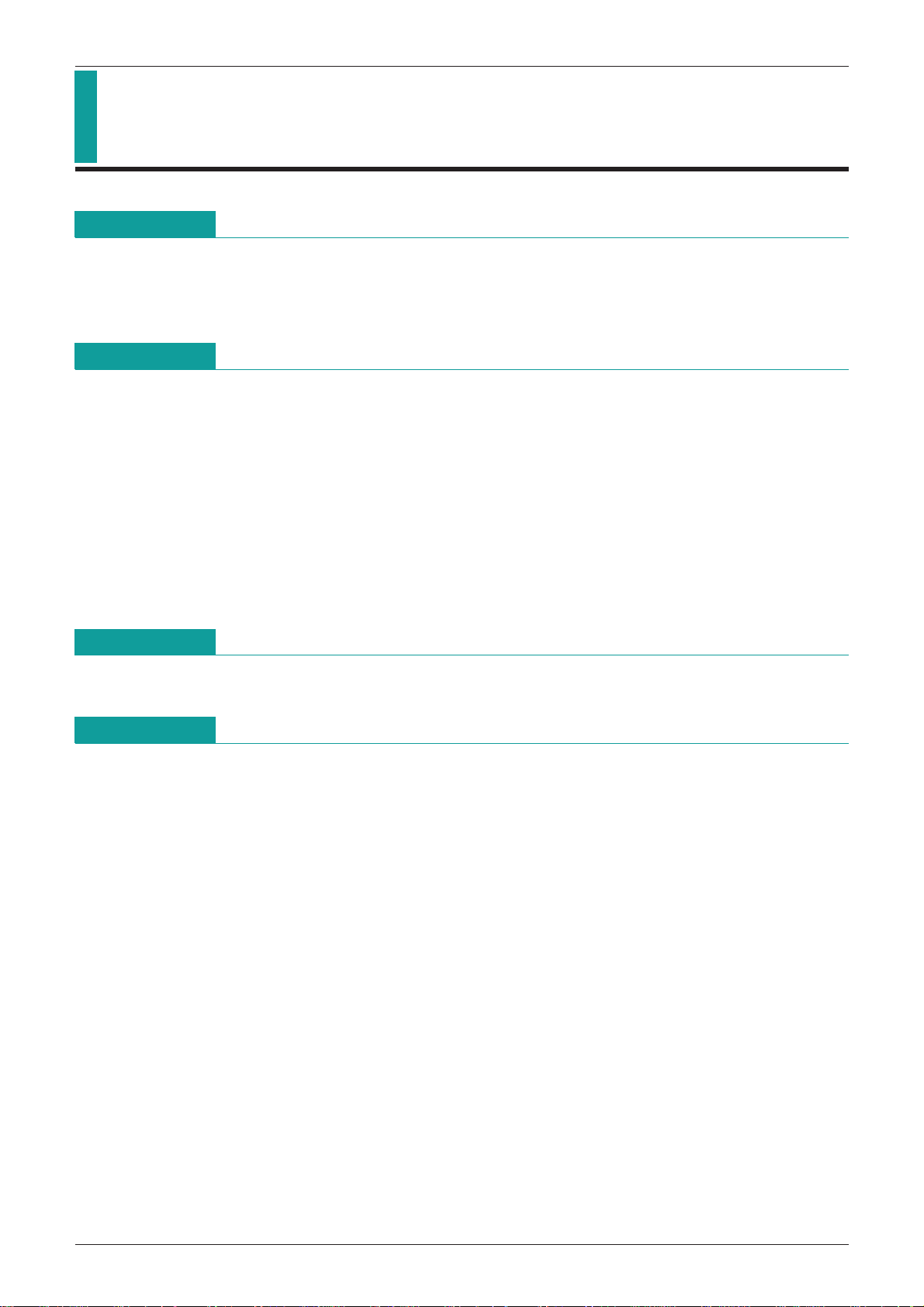
Monolithic IC MM1407
Outline
This audio IC was developed for notebook PCs and allows major reduction of amp circuit board area. (To
conform to PC98, includes built-in speaker drive amp, headphone amp, line amp. stereo/monaural switching,
DC voltage control electronic volume, watchdog, logic control function.)
Features
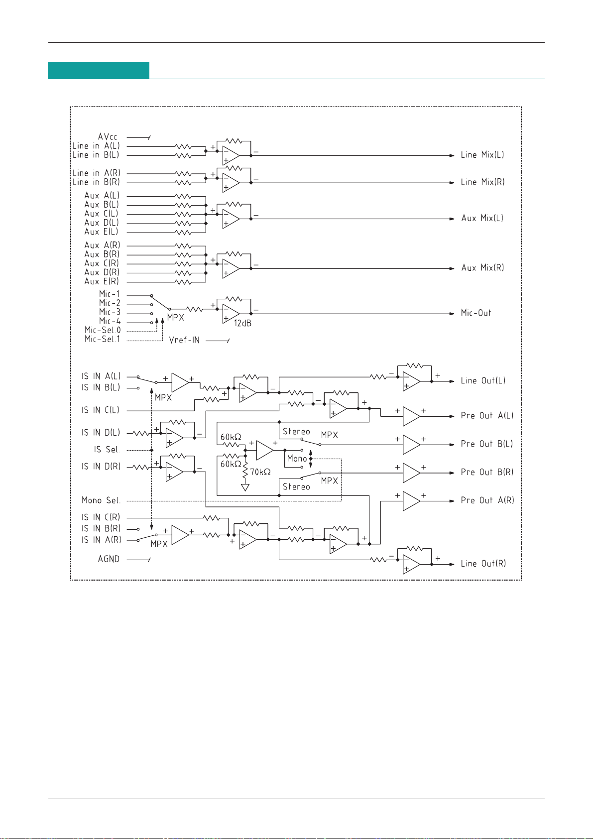
(1) Speaker amp: Stereo BTL output 0.7W (when VCC = 5.0V, RL = 8Ω)
(2) Electronic volume control (
THD1 = 0.5% (when V
THD2 = 0.1% (when V
(4) Line amp: Mixes 4 inputs ( 2ch signals and outputs on 3 outputs ( 2ch. Stereo/monaural switching
possible on one line. THD = 0.1% (when V
(5) Microphone amp: Switch pin selects 1 of 4 inputs
(6) Logic control: Speaker, headphone and line amp (including microphone amp and mix amp) logic
controllable. Current consumption 300µA during power save mode.
-
60 ~ +20dB). THD = 0.5% (when POUT = 300mW, RL = 8Ω)
OUT = 100mVrms, RL = 16Ω)
OUT = 1VmVrms, RL = 10kΩ)
OUT = 1Vrms, RL = 10kΩ)
Package
QFP-80B
Applications
(1) Notebook PC audio control
Page 2
MITSUMI
Block Diagram
Audio signal control section
(Except where otherwise indicated amp gain is 0dB.)
Audio MM1407
Page 3
MITSUMI
Audio MM1407
HP signal control section
SP signal
control
section
Digtal signal
control section
Page 4
MITSUMI
Pin Description
Audio MM1407
60 57 5559 58 56 53952
54
61
62
63
64
65
66
67
68
69
70
71
72
73
74
75
76
77
78
79
80
13 762458
105111501249134814471546164517441843194220
QFP-80B
41
40
39
38
37
36
35
34
33
32
31
30
29
28
27
26
25
24
23
22
21
1 Vref-IN 21 IS IN A (R) 41 HP (R) 61 HP IN (L)
2 Aux E (L) 22 IS IN B (R) 42 V
CC1 62 IS IN E (L)
3 Aux D (L) 23 IS IN C (R) 43 PGND1 63 SP IN (L)
4 Aux C (L) 24 IS IN D (R) 44 SP (R)+ 64 HP VOL
5 Aux B (L) 25 IS SEL 45 VP1 65 Mic
6 Aux A (L) 26 Line out (R) 46 VP2 66 Mic
7 Aux Mix (L) 27 Pre out A (R) 47 SP (R)
-
67 Mic-1
8 Line in B (L) 28 Pre out B (R) 48 PGND2 68 Mic
9 Line in A (L) 29 Mono SEL 49 GND1 69 Mic
10 Line Mix (L) 30 Cap 50 GND2 70 Mic
-
sel 0
-
sel 1
-
2
-
4
-
3
11 AGND1 31 WAKEUP 51 PGND3 71 Mic out
12 Line Mix (R) 32 AMPSD 52 SP (L)+ 72 AGND2
13 Line in A (R) 33 SD 53 VP3 73 Pre out B (L)
14 Line in B (R) 34 HP
15 Aux Mix (R) 35 DGND 55 SP (L)
16 Aux A (R) 36 VD 56 PGND4 76 AV
-
IN 54 VP4 74 Pre out A (L)
-
75 Line out (L)
CC
17 Aux B (R) 37 Vref (P)-IN 57 VCC2 77 IS IN D (L)
18 Aux C (R) 38 SP IN (R) 58 HP (L) 78 IS IN C (L)
19 Aux D (R) 39 IS IN E (R) 59 IS IN E VOL 79 IS IN B (L)
20 Aux E (R) 40 HP IN (R) 60 SP VOL 80 IS IN A (L)
Page 5
MITSUMI
Pin Description
Audio MM1407
Pin No.
Pin name
1 Vref
2 Aux E (L) Input Audio signal control 1 of 5 Aux Mix (L) (add amp) inputs.
3 Aux D (L) Input Audio signal control 1 of 5 Aux Mix (L) (add amp) inputs.
4 Aux C (L) Input Audio signal control 1 of 5 Aux Mix (L) (add amp) inputs.
5 Aux B (L) Input Audio signal control 1 of 5 Aux Mix (L) (add amp) inputs.
6 Aux A (L) Input Audio signal control 1 of 5 Aux Mix (L) (add amp) inputs.
7
Aux Mix (L)
8
Line In B (L)
9
Line In A (L)
10
Line Mix (L)
11 AGND1 GND Audio signal control
12
Line Mix (R)
13
Line In A (R)
14
Line In B (R)
15
Aux Mix (R)
16 Aux A (R) Input Audio signal control 1 of 5 Aux Mix (R) (add amp) inputs.
17 Aux B (R) Input Audio signal control 1 of 5 Aux Mix (R) (add amp) inputs.
18 Aux C (R) Input Audio signal control 1 of 5 Aux Mix (R) (add amp) inputs.
19 Aux D (R) Input Audio signal control 1 of 5 Aux Mix (R) (add amp) inputs.
20 Aux E (R) Input Audio signal control 1 of 5 Aux Mix (R) (add amp) inputs.
21 IS IN A (R) Input Audio signal control
22 IS IN B (R) Input Audio signal control
23 IS IN C (R) Input Audio signal control
24 IS IN D (R) Input Audio signal control
25 IS Sel. Input (SW) Audio signal control
26
Line Out (R)
27
Pre Out A (R)
28
Pre Out B (R)
29 Mono Sel. Input (SW) Audio signal control
30 Cap
31 WAKEUP
32 AMPSD
33 SD
-
IN
Input/Output
Power supply
(reference)
Output Audio signal control Signal with Aux A ~ E (L) input added is output.
Input Audio signal control 1 of 2 Line In (L) (add amp) inputs.
Input Audio signal control 1 of 2 Line In (L) (add amp) inputs.
Output Audio signal control Signal with Aux A ~ B (L) input added is output.
Output Audio signal control Signal with Aux A ~ B (L) input added is output.
Input Audio signal control 1 of 2 Line In (R) (add amp) inputs.
Input Audio signal control 1 of 2 Line In (R) (add amp) inputs.
Output Audio signal control Signal with Aux A ~ E (R) input added is output.
Output Audio signal control
Output Audio signal control
Output Audio signal control
Input (logic)
Input (logic)
Input (logic)
Input (logic)
Section Function
Audio signal control Applies audio signal control reference potential.
Audio signal control ground pin. (except for Mic amp)
1 pin of 4 amp inputs that output to Line Out (R), Pre Out
A (R), Pre Out B (R), (L).
1 pin of 4 amp inputs that output to Line Out (R), Pre Out
A (R), Pre Out B (R), (L).
1 pin of 4 amp inputs that output to Line Out (R), Pre Out
A (R), Pre Out B (R), (L).
1 pin of 4 amp inputs that output to Pre Out A (R), Pre
Out B (R), (L).
This pin selects either of two inputs IS IN A (R) or IS IN
B (R). (See Figure A)
A signal that has IS IN A (R) or B (R) or IS IN C (R)
added is output.
A signal that has IS IN A (R) or B (R) or IS IN C (R) or
IS IN D (R) added is output.
During Mono Sel. R Stereo selection, a signal that has IS IN A
(R) or B (R) or IS IN C (R) or IS IN D (R) added is output.
During Mono Sel. R Mono selection, a signal that is a mixture of
a signal with (R) input added and then lowered 9dB and a signal
that with (L) input added and lowered 9dB.
This pin switches Pre Out B (L), (R) Stereo and Mono
output. (See Figure A)
This pin sets clock monitoring time for the watchdog timer
Digital signal control
Digital signal control 1 of 4 logic circuit inputs. (See Figure D)
Digital signal control 1 of 4 logic circuit inputs. (See Figure D)
Digital signal control 1 of 4 logic circuit inputs. (See Figure D)
circuit. Clock monitoring time is determined by the capacitor
time constant connected to this pin. (See Figure C)
Page 6
MITSUMI
Audio MM1407
Pin No.
Pin name
34 HP
35 DGND GND
36 VD
37 Vref
38 SP IN (R) Input SP signal control
39 IS IN E (R) Input SP signal control
40 HP IN (R) Input HP signal control HP amp (R
41 HP (R) Output HP signal control HP amp (R
42 V
43 PGND1 GND
44 SP (R) + Output SP signal control SP amp (R
45 VP1
46 VP2
47 SP (R)
48 PGND2 GND
49 GND1 GND
50 GND2 GND
51 PGND3 GND
52 SP (L) + Output SP signal control SP amp (L
53 VP3
54 VP4
55 SP (L)
56 PGND4 GND
57 V
58 HP (L) Output HP signal control HP amp (R
59 IS IN E Vol. Input SP signal control SP amp IS IN E input electronic volume pin. (
60 SP Vol. Input SP signal control SP amp SP IN input electronic volume pin. (
61 HP IN (L) Input HP signal control HP amp (L
62 IS IN E (L) Input SP signal control
63 SP IN (L) Input SP signal control
64 HP Vol. Input HP signal control HP amp electronic volume pin. (
65 Mic
66 Mic
67 Mic
68 Mic
69 Mic
70 Mic
71 Mic
-
-
(P) IN
CC1
CC2
-
Sel.0 Input Audio signal control
-
Sel.1 Input Audio signal control
-
Input/Output
IN
Input (logic) Digital signal control
Power supply
Power supply
(reference)
Power supply
Power supply
Power supply
-
Output SP signal control SP amp (R-ch) BTL output (-) pin.
Power supply
Power supply
-
Output SP signal control SP amp (L-ch) BTL output (-) pin.
Power supply
-
1 Input Audio signal control 1 of 4 Mic amp inputs.
-
2 Input Audio signal control 1 of 4 Mic amp inputs.
-
4 Input Audio signal control 1 of 4 Mic amp inputs.
-
3 Input Audio signal control 1 of 4 Mic amp inputs.
Out Output Audio signal control
Section Function
1 of 4 logic circuit inputs. (See Figure D)
Digital signal control
Digital signal control
SP, HP signal control Applies SP, HP signal control section reference potential.
SP, HP signal control
SP, HP signal control
SP, HP signal control
SP, HP signal control
SP, HP signal control
SP, HP signal control
SP, HP signal control
SP, HP signal control
SP, HP signal control
SP, HP signal control
SP, HP signal control
SP, HP signal control
Digital signal control ground pin.
Digital signal control Vcc pin. (*1)
1 of 2 SP amp (R
input.
1 of 2 SP amp (R
input.
SP, HP amp input stage, EVR circuit, DC bias circuit VCC
pin. (*2)
SP, HP amp output stage (power amp) ground pin.
SP, HP amp output stage (power amp) VCC pin.
SP, HP amp output stage (power amp) VCC pin.
SP, HP amp output stage (power amp) ground pin.
SP, HP amp input stage, EVR circuit, DC bias circuit
ground pin. (
SP, HP amp input stage, EVR circuit, DC bias circuit
ground pin. (
SP, HP amp output stage (power amp) ground pin.
SP, HP amp output stage (power amp) VCC pin.
SP, HP amp output stage (power amp) VCC pin.
SP, HP amp output stage (power amp) ground pin.
SP, HP amp input stage, EVR circuit, DC bias circuit Vcc
pin. (
1 of 2 SP amp (L
input.
1 of 2 SP amp (L
input.
Selects 1 of 4 Mic amp inputs in combination with Mic-
Sel. 1 pin. (See Figure E)
Selects 1 of 4 Mic amp inputs in combination with Mic-
Sel. 0 pin. (See Figure E)
1 of 4 Mic 1 ~ 4 inputs is output depending on
combination of Mic Sel. 0 and Mic Sel. 1 pins.
2)
*
-
ch) inputs. Use music source, etc.
-
ch) inputs. Use beep alarm sound, etc.
-
ch) input.
-
ch) output.
-
ch) BTL output (+) pin.
3)
*
3)
*
-
ch) BTL output (+) pin.
-
ch) output pin.
-
ch) input.
-
ch) inputs. Use beep alarm sound, etc.
-
ch) inputs. Use music source, etc.
6)
*
4)
*
5)
*
Page 7
MITSUMI
Audio MM1407
Pin No.
1 VD power supply and VP power supply must have the same potential.
*
2 In order to avoid the effects of SP, HP amp interference between L and R, and interference between SP
*
3 In order to avoid the effects of SP, HP amp interference between L and R, and interference between SP
*
4 The maximum voltage that can be impressed on IS IN E Vol. pin is 2.0V.
*
5 The maximum voltage that can be impressed on SP Vol. pin is 2.0V.
*
6 The maximum voltage that can be impressed on HP Vol. pin is 2.0V.
*
Pin name
72 AGND2 GND Audio signal control Mic amp ground pin.
73
Pre Out B (L)
74
Pre Out A (L)
75
Pre Out (L)
76 AV
77 IS IN D (L) Input Audio signal control
78 IS IN C (L) Input Audio signal control
79 IS IN B (L) Input Audio signal control
80 IS IN A (L) Input Audio signal control
and HP amps on separation characteristics, the wiring connected to this pin should have the same
impedance as other Vcc lines (especially lines with large current). (This is not a problem when Vcc1 and
Vcc2 lines are bundled.)
and HP amps on separation characteristics, the wiring connected to this pin should have the same
impedance as other ground lines (especially lines with large current). (This is not a problem when GND1
and GND2 lines are bundled.)
Input/Output
Output Audio signal control
Output Audio signal control
Output Audio signal control
CC Audio signal control Audio signal control VCC pin.
Section Function
During Mono Sel. R Stereo selection, a signal that has IS IN A (L)
or B (L) or IS IN C (L) or IS IN D (L) added is output. During
Mono Sel. R Mono selection, a signal that is a mixture of a signal
with (L) input added and then lowered 9dB and a signal that with
(R) input added and lowered 9dB. (See Figure B)
A signal that has IS IN A (R) or B (R) or IS IN C (R) or
IS IN D (R) added is output.
A signal that has IS IN A (R) or B (R) or IS IN C (R)
added is output.
1 of 4 amp inputs that is output to Pre Out A (R) or Pre
Out B (R), (L).
1 of 4 amp inputs that is output to Line Out (R) or Pre
Out A (R), Pre Out B (R), (L).
1 of 4 amp inputs that is output to Line Out (R) or Pre
Out A (R), Pre Out B (R), (L).
1 of 4 amp inputs that is output to Line Out (R) or Pre
Out A (R), Pre Out B (R), (L).
Page 8
MITSUMI
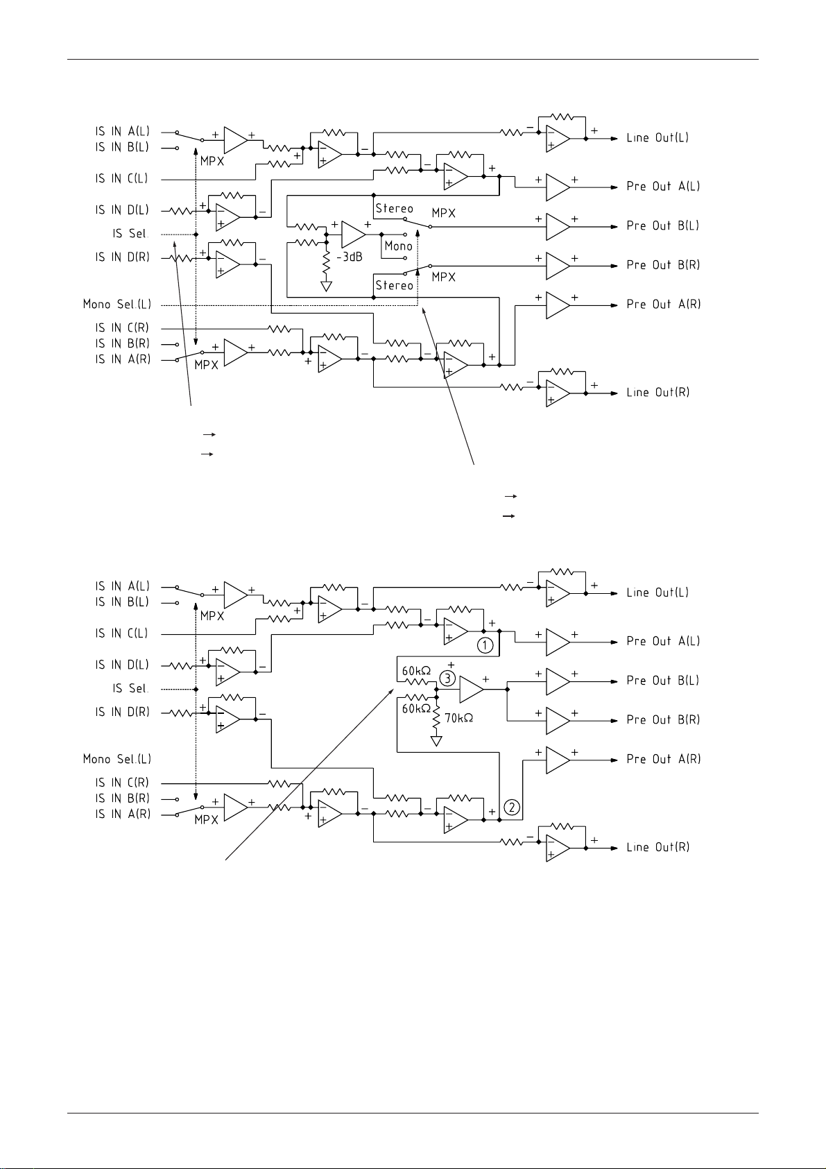
IS Sel. Pin and Mono Sel. (L) Pin Selection
Selects either IS IN A (R) or IS IN B (L).
IS SEL. H A
L B
Audio MM1407
Selects either Pre Out B (L), (R) Stereo/Monaural.
Mono Sel. (L) H Stereo
L Monaural
Figure B. Mono Sel. (L) Pin Pre Out B (L) (R) Signal Route during Mono Selection
The signal route when Mono Sel. (L) pin mono is selected is: point 1 L-ch signal
is lowered 9dB and this signal is added at point 3 to point 2 R-ch signal lowered
9dB.
This level is output to Pre Out B (L), (R).
Page 9

MITSUMI
Mono Sel. (L) Pin Pre Out B (L) (R) Signal Route during Stereo Selection
During Mono Sel. 1 pin stereo selection, the signal at point 1
is output to Pre Out B (L) and the signal at point 2 is output
to Pre Out B (R).
Audio MM1407
Mic-Sel. 0, Mic-Sel. 1 pin selection
1 of 4 Mic 1~4 inputs is selected by Mic-Sel. 0 and Mic-Sel. 1.
Mic-Sel. 0 Mic-Sel. 1
Mic 1 L L
Mic 2 L H
Mic 3 H L
Mic 4 H H
Page 10

MITSUMI
Figure C. Watchdog Timer
Audio MM1407
Watchdog Timer Circuit Block Diagram
Basically, the watchdog timer monitors the level (3) of the current it impresses on the external capacitor. The
charging time is determined by C1 and I2 in the block diagram, and control is done by input signal (1). When
the first "H" trigger (input signal) chargers the external capacitor and level (3) goes over (4) "H" threshold
value, output is first inverted (L H). While the input signal is being continuously impressed, the timer repeats
charging current impress/stop to the external capacitor, but if input signal (1) is not impressed within the set
time (clock monitoring time), charging to the external capacitors is stopped and the capacitor starts discharge
operation. Then level (3) falls below "L" threshold value and output (5) is again inverted (H L).
1. WAKEUP pin input signal cycle limit
Use at 1/Ta or higher, 100Hz or lower.
T1: clock monitoring time (The time from WAKEUP signal input stop until logic truth table WAKEUP
switches to low.)
2. WAKEUP pin input signal amplitude limit
Use at 1.5V or higher, 5V or lower.
3. External capacitor time constant (sets clock monitoring time)
Determined by T1 = 1.638 C µF R [Ω].
(E.g.: If C = 1µF, for T1 .=
1S, R = 620kΩ, for T1
.
.
=
2S, R = 1.2MΩ)
.
Page 11

MITSUMI
Audio MM1407
Logic Truth Table
#SD #AMPSD WAKEUP HP-IN CHIP-EN #SP-EN #HP-EN SW
(1) H H EN EN EN OFF
(2) H L EN EN DIS ON
(3) H H L H EN DIS EN ON
(4) H H L L EN EN DIS ON
(5) H L L EN DIS DIS ON
(6) L L DIS DIS DIS ON
· WAKEUP "H" indicates the state where a pulse is impressed continuously, and "L" means that pulse
impression is stopped and level is low. (See Figure C)
· The EN in CHIP-EN means that the audio signal control section in the block diagram is ON, and DIS means
that it is OFF.
· The EN in #SP-EN means that the SP signal control section in the block diagram is ON, and DIS means that
it is OFF.
· The EN in #HP-EN means that the HP signal control section in the block diagram is ON, and DIS means that
it is OFF.
· SW ON and OFF: ON means that SP IN and IS IN E in the SP signal control section in the block diagram are
both operating, and OFF means that IS IN E only is operating.
Absolute Maximum Ratings
Item Signal Rating Unit
Storage temperature T
Operating temperature T
Power supply voltage (AV
Power supply voltage (VP) V
Power supply voltage (VD) V
Input pin voltage (AV
Input pin voltage (VP) V
Input pin voltage (VD) V
Allowable loss Pd
When used at over 25, there is a 14mW reduction for every 1°C.
*
(Mounting conditions: 40 40 1.6mm. Glass epoxy, board mounting density 30%.)
CC) VINmax.1
(Ta = 25°C )
STG
OPR
CC) VCCmax.1 7 V
CCmax.2 7 V
CCmax.3 7 V
INmax.2
INmax.3
-
40~+125 °C
-
20~+75 °C
-
0.3~AVCC+0.3 V
-
0.3~VP+0.3 V
-
0.3~VD+0.3 V
680mW (alone)
1.6W (mounted on board)
W
Page 12

MITSUMI
Audio MM1407
Recommended Operating Conditions
(Ta = 25°C)
Item Signal Rating Unit
Operating temperature T
Operating voltage (AV
Operating voltage (VP) V
Operating voltage (VD) V
Electrical Characteristics
CC) VCCop1 4.5~5.5 V
(Except where otherwise indicated, Ta = 25°C, AVCC = VP = VD = 5V)
OPR
CCop2 4.5~5.5 V
CCop3 4.5~5.5 V
-
20~+75 °C
Item Signal Measurement conditions Min. Typ. Max. Unit
Consumption Current
Audio signal control I
HP AMP operating I
SP AMP operating I
During power save I
Audio signal control Hereafter R
Maximum output voltage Vmax.1
Distortion rate THD1
Gain 1 Gv1
CC1 For HP AMP, SP AMP OFF 8 12 mA
CC2 For Audio ON, SP AMP OFF 18 27 mA
CC3 For Audio ON, HP AMP OFF, no load 38 57 mA
CC4 300 500 µA
L = 10k, fIN = 1kHz
Line Out (L, R) , Aux Mix (L, R) , Line Mix (L, R)
Mic Out THD = 1%
1 1.1 Vrms
Line Out (L, R) , Aux Mix (L, R) , Line Mix (L, R)
Mic Out VOUT = 1Vrms
Line Out (L, R) , Aux Mix (L, R) , Line Mix (L, R)
Gain 2 Gv2 Mic Out 12 dB
Input impedance R
IN 47 kΩ
Impedance may change during power save, but it will not go below 47k Ω.
Signal coupling on input pins may be observed.
Output impedance R
OUT 100 Ω
Separation CS 60 dB
Output offset 1 V
Output offset 2 (MIC AMP) V
OFF1(VOUT)
OFF218mV
-
(Vref-VIN) 1 8 mV
R-Rejection SVRR fr=100Hz 70 85 dB
Output noise voltage Vno 20Hz ~ 20kHz, A curve 30 100
Phase Relationships
Line in to Line Mix Inverted
Aux A ~ E to Aux Mix Inverted
Mic A ~ D to Mic Out Inverted
IS IN A ~ D to Line Out Non-inverted
IS IN A ~ D to Pre Out Non-inverted
IS IN A ~ D to Pre Out phase relationships does not change for Mono Select R Mono or Stereo
0.1 %
0dB
µVrms
Page 13

MITSUMI
Item Signal Measurement conditions Min. Typ. Max. Unit
Headphone AMP Hereafter R
Maximum output voltage 1 Vmax.hp1
Maximum output voltage 2 Vmax.hp2
Distortion rate 1 THDhp1
Distortion rate 2 THDhp2
Gain 1 Ghp1 EVR; for max. (Vvol1 = 1.25V) 0 dB
Gain 2 Ghp2 EVR; (Vvol1 = 1.0V)
Gain 3 Ghp3 EVR; (Vvol1 = 0.85V)
Gain 4 Ghp4 EVR; (Vvol1 = 0.75V)
Gain 5 Ghp5
Output level
temperature characteristic
Between-channel
gain difference 1
Between-channel
gain difference 2
R-Rejection SVRRhp
Output noise voltage Vnohp EVR = 0dB, 20Hz~20kHz, A curve 175
Separation CShp EVR = 0dB, fr = 1kHz 50 65 dB
Speaker AMP Hereafter R
L = 8Ω, BTL connected, fIN = 1kHz
Maximum output power Pmax.sp
Distortion rate THDsp
Gain 1 Gsp1 EVR; for max. (Vvol = 1.25V) 20 dB
Gain 2 Gsp2 EVR; (Vvol1 = 1.0V) 0 dB
Gain 3 Gsp3 EVR; (Vvol1 = 0.85V)
Gain 4 Gsp4 EVR; (Vvol1 = 0.75V)
Gain 5 Gsp5
Output level
temperature characteristic
Between-channel
gain difference 1
Between-channel
gain difference 2
R-Rejection SVRRsp
Output offset V
Output noise voltage Vnosp
Separation CSsp EVR = 20dB, fr = 1kHz 50 65 dB
Audio MM1407
L = 16Ω, fIN = 1kHz
PreOutA (L, R) HP IN (L, R) ,
R
L = 10kΩ, THD = 1%
PreOutA (L, R) HP IN (L, R) ,
L = 16Ω, THD = 1%
R
PreOutA (L, R) HP IN (L, R)
EVR = 0dB V
OUT = 1Vrms, RL = 10kΩ
PreOutA (L, R) HP IN (L, R)
EVR = 0dB, V
EVR; V
OUT = 100mVrms, RL = 16Ω
IN = 0dBV for MIN (Vvol = 0.6V)
Mute when Vvol = 0.6V or below
EVR setting; gain 1
1 1.1 Vrms
350
mVrms
0.13 0.25 %
1%
-
20 dB
-
40 dB
-
60 dB
-
80 dB
+3000
ppm/
CBhp1 EVR setting; gain 1 ~ 2 ±1 dB
CBhp2 EVR setting; gain 3 ~ 4 ±3 dB
EVR = 0dB, fr = 100Hz,
V
RIPPLE =
-
20dBV
50 65 dB
µVrms
PreOutB (L, R) SP IN (L, R) ,
THD = 10%, EVR = 20dB
PreOutB (L, R) SP IN (L, R) , EVR = 20dB
POUT = 300mW
EVR; V
IN = 0dBV for MIN (Vvol = 0.6V)
Mute when Vvol = 0.6V or below
EVR setting; gain 1 +3000
0.7 W
13%
-
20 dB
-
40 dB
-
60 dB
ppm/°C
CBsp1 EVR setting; gain 1 ~ 2 ±1 dB
CBsp2 EVR setting; gain 3 ~ 4 ±3 dB
EVR = 20dBV, fr = 100Hz, V
OFFsp IS IN E VOL = min. SP VOL = 20dB 0 150 mV
IS IN E VOL = SP VOL = 20dB,
20Hz~20kHz, A curve
RIPPLE
= -20dBV
38 45 dB
560
µVrms
°C
Page 14

MITSUMI
Measuring Circuit
ICC1, ICC2, ICC3, ICC4
Audio MM1407
Page 15

MITSUMI
Vmax1, THD1, Gv1, Gv2
Audio MM1407
Page 16

MITSUMI
Voff1, Voff2, SVRR, Vno
Audio MM1407
Page 17

MITSUMI
CS
Audio MM1407
Page 18

MITSUMI
Vmaxhp1, Vmaxhp2, THDhp1, THDhp2, Ghp1~5, CBhp1~2
Audio MM1407
Page 19

MITSUMI
SVRRhp, Vnohp
Audio MM1407
Page 20

MITSUMI
CShp
Audio MM1407
Page 21

MITSUMI
Pmaxsp, THDsp, Gsp1~5, CBsp1~2
Audio MM1407
Page 22

MITSUMI
SVRRsp, Vnosp
Audio MM1407
Page 23

MITSUMI
Voffsp
Audio MM1407
Page 24

MITSUMI
0.01
0.001
0.01
0.1
1
10
0.1 1 10
VOUT (Vrms)
THD (%)
0.01 0.1
1
10
0.001
0.01
0.1
1
10
VOUT (Vrms)
THD (%)
CSsp
Audio MM1407
Measuring Circuit
THD Aux-A (L) AuxMix (L)
Mic-a Micont
Page 25

MITSUMI
0.01
0.001
0.01
0.1
1
10
0.1 1 10
VOUT (Vrms)
THD (%)
0.01
0.001
0.01
0.1
1
10
0.1 1 10
VOUT (Vrms)
THD(%)
EVR=-10dB
EVR=0dB
0.01
0.01
0.1
1
10
100
0.1 1 10
VOUT (V)
THD (%)
EVR=0dB
0.01
0.01
0.1
1
10
0.1 1 10
VOUT (Vrms)
THD (%)
0 0.2 0.4 0.6 0.8 1 1.2 1.4 1.6 1.8 2
-
100
-
80
-
60
-
40
-
20
0
20
Vvo1 (V)
Gain (dB)
0 0.2 0.4 0.6 0.8 1 1.2 1.4 1.6 1.8 2
0
10
20
30
40
50
60
70
80
90
Noise (µVrms)
HP Vol. (V)
0 0.2 0.4 0.6 0.8 1 1.2 1.4 1.6 1.8 2
-
100
-
80
-
60
-
40
-
20
0
20
40
Vvo1 (V)
Gain (dB)
0 0.2 0.4 0.6 0.8 1 1.2 1.4 1.6 1.8 2
100
110
120
130
140
150
160
170
180
190
SP Vol. (V)
Noise (µVrms)
Audio MM1407
Line in A (L) LineMix (L)
THD IS IN A (L) Per Out A (L) HP IN (L) HP (L) R
L
=16Ω
THD IS IN A (L) LineOUT (L)
THD IS IN A (L) Per Out A (L) HP IN (L) HP (L) R
L
=10kΩ
EVR-GAIN HP AMP
EVR-GAIN SP AMP
EVR-NOISE HP AMP
EVR-NOISE SP AMP (IS IN E Vol. = 1.25V, SP Vol. Variable)
 Loading...