

Page 1

MITSUMI
MITSUMI
NTSC/PAL Encoder MM1394
NTSC/PAL Encoder
Monolithic IC MM1394
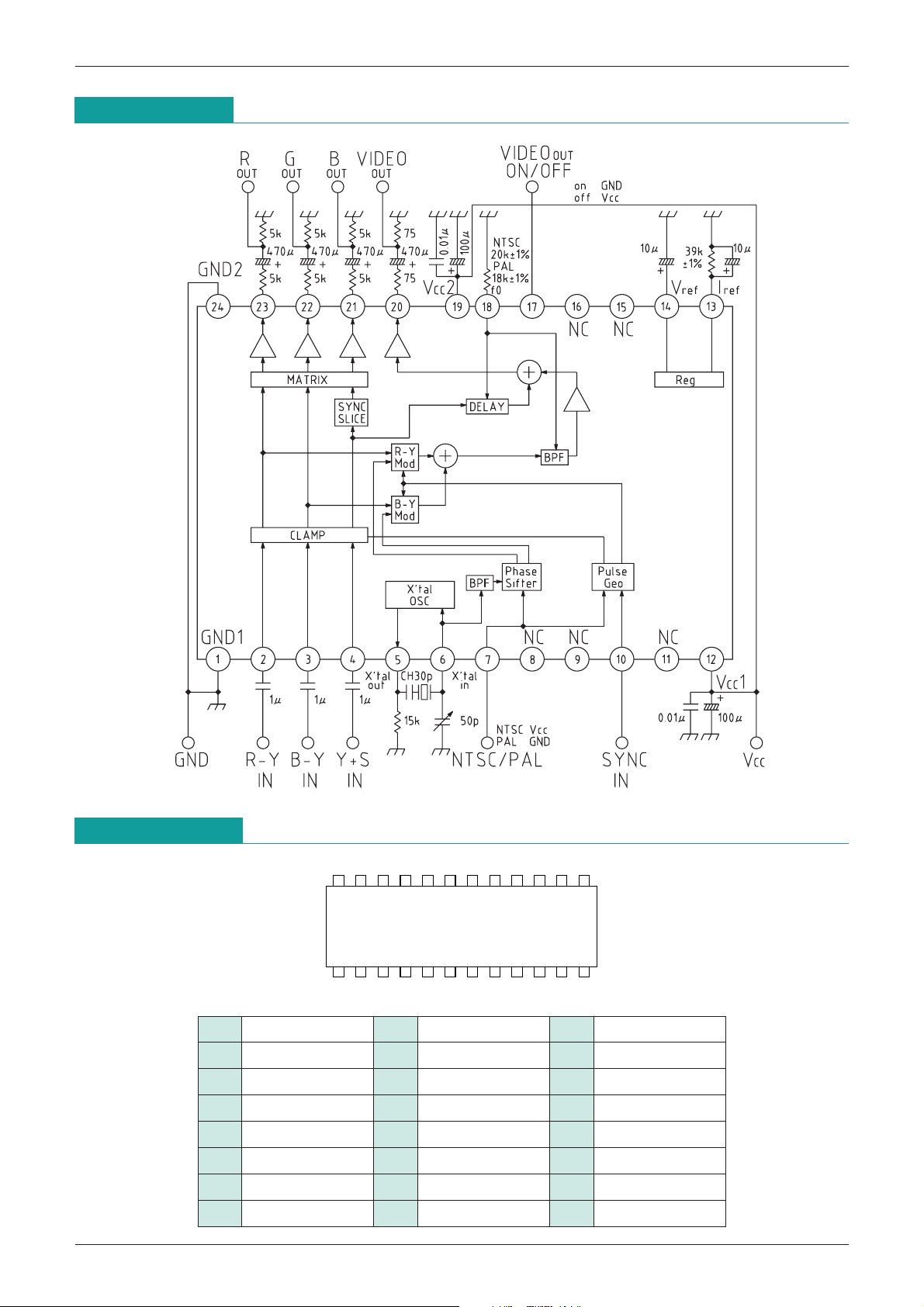
Outline
This is an encoder IC that converts luminance signal Y, color difference signals R-Y and B-Y to composite
video signals and RGB signals.
Features
1. Operates on 5V single power supply
2. Low power consumption (265mW : video output ON)
(165mW : video output OFF)
3. Supports both NTSC and PAL formats
4. Built-in 75Ω drive output (RGB output, composite output)
5. BPF and DELAY filters built-in
6. Built-in oscillator for subcarrier
7. Built-in video output ON/OFF circuit
Package
SOP-24
Applications
1. Game equipment
2. Digital cameras
3. Other video equipment
Page 2
MITSUMI
SOP-24
136924587101211
24 20 1723 21 19 18 1622 131415
Block Diagram
NTSC/PAL Encoder MM1394
Pin Assignment
1 GND1 9 NC 17
2 R-Y IN 10 SYNC IN 18 f0
3 B
4 Y+S
5 X' tal OUT 13 Iref 21 B OUT
6 X' tal IN 14 Vref 22 G OUT
7 NTSC/PAL 15 NC 23 R OUT
8 NC 16 NC 24 GND2
-
Y IN 11 NC 19 VCC2
IN 12 VCC1 20 VIDEO OUT
VIDEO
OUT
ON/OFF
Page 3
MITSUMI
MITSUMI
NTSC/PAL Encoder MM1394
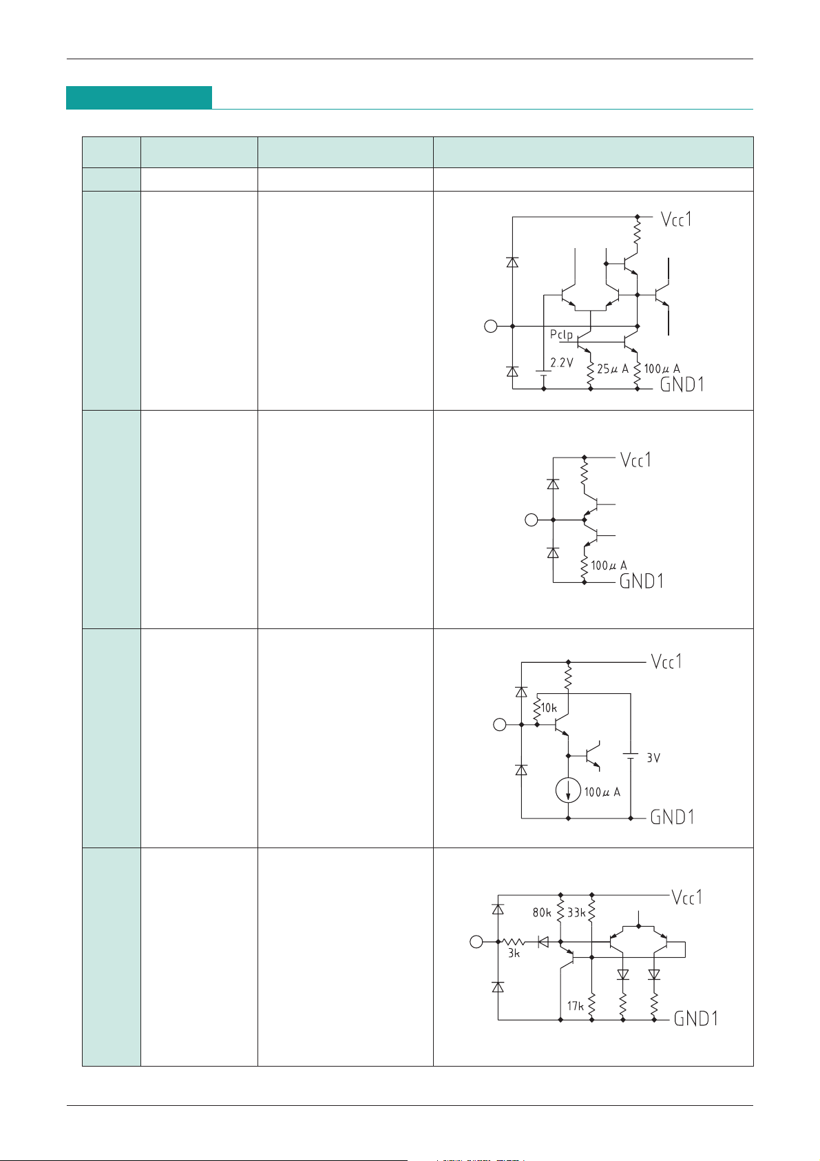
Pin Description
Pin no. Pin name Function Internal equivalent circuit diagram
1 GND1
2 R-YIN Input pins.
3 B
4 Y+S
-
YIN Maximum input voltage :
IN R
-
Y 1.00VP
B-Y 1.27VP
Y+S 1.00VP
-
P
-
P
-
P
(SYNC is 0.286VP
-
P)
DC level for clamp is 2.2V.
5 X' tal OUT Oscillator circuit output pin
6 X' tal in Subcarrier input pin
Input a 0.4~1.0V
P-P
sine wave.
7 NTSC/PAL Mode setting pin
NTSC : V
CC
PAL : PAL
Page 4

MITSUMI
MITSUMI
NTSC/PAL Encoder MM1394
Pin no. Pin name Function Internal equivalent circuit diagram
8
NC OPEN
9
10 SYNC IN Composite sync signal
input pin
11 NC OPEN
12 VCC1
13 Iref
Determines internal
reference current.
Connect a 47kΩ resistor
between this pin and GND.
14 Vref Internal reference voltage
pin
Reference voltage : 4V
Connect a 10µF capacitor
between this pin and GND.
15
16
NC OPEN
Page 5

MITSUMI
NTSC/PAL Encoder MM1394
Pin no. Pin name Function Internal equivalent circuit diagram
17 VIDEO OUT
Turns VIDEO output ON/OFF
ON/OFF VIDEO output ON : GND
OFF : V
CC
18 f0 Determines f0 for filter and
delay circuits.
NTSC : 20k
PAL : 16k
19 VCC2
Output stage power supply
20 VIDEO OUT Composite video signal
output pin
Can drive 75Ω load.
21 BOUT
22 GOUT RGB signal output pin
23 B
OUT
24 GND2 Output stage GND
Page 6

MITSUMI
NTSC/PAL Encoder MM1394
Absolute Maximum Ratings
(Ta=25°C)
Item Symbol Ratings Units
Storage temperature T
Operating temperature T
Power supply voltage V
CC max. +7 V
Allowable loss Pd 450 mW
Recommended Operating Conditions
Item Symbol Ratings Units
Operating temperature T
Operating power supply V
Electrical Characteristics
Item
Consumption current 1 I
Consumption current 2 I
RGB output characteristics
R output voltage VR D
G output voltage VG C
B output voltage VB B
Rf characteristic fR D
Gf characteristic fG C SW (1, 1, 0, 0, 1, 0, 0)
Bf characteristic fB B
Red-1 level ratio
Red-1 phase
Red-2 level ratio
Red-2 phase
Green-1 level ratio
Green-1 phase
Green-2 level ratio
Green-2 phase
Blue-1 level ratio
Blue-1 phase
Blue-2 level ratio
Blue-2 phase
NTSC / PAL
Burst position td
Burst width tw
Carrier leak VL A V4 : SG6 V5 : SG8 30
Oscillation circuit
(Except where noted otherwise, Ta=25°C, VCC=5.0V)
Symbol
Measurement
pin
CC1
CC2
CL (R1)
CP (R1)
CL (R2)
CP (R2)
CL (G1)
CP (G1)
CL (G2)
A
CP (G2)
CL (B1)
CP (B1)
CL (B2)
CP (B2)
A V4 : SG6 V5 : SG8
STG
OPR
OPR
OPR 4.75~5.25 V
-
40~+125 °C
-
20~+75 °C
-
20~+75 °C
Measurement conditions
SW conditions Min. Typ. Max. Units
SW (S1,S2,S3,S4,S5,S6,S7)
V4 : SG6 V5 : SG8
SW (0, 0, 0, 0, 0, 0, 0)
V4 : SG6 V5 : SG8
SW (0, 0, 0, 0, 0, 1, 0)
V1 : SG3 V2 : SG4 V3 : SG5
SW (1, 0, 0, 0, 0, 0, 0)
0.64 0.71 0.78 V
V3 : SG2/SG1 V4 : SG6
R, B frequency response Va=2.0V
-
G frequency response Va=2.9V
*
2.62 2.92 3.21
2.62 2.92 3.21
2.46 2.56 2.66
2.46 2.74 3.02
231 241 251
2.46 2.74 3.02
109 119 129
1.87 2.08 2.29
337 347 357
1.87 2.08 2.29
V1 : SG3 V2 : SG4 V3 : SG5
SW (1, 0, 0, 0, 0, 0, 0)
V1, 2, 3 : no signal
*
6
0.4 0.6 0.75 µS
2.3 2.55 3.0 µS
SW (1, 0, 0, 0, 0, 0, 0) *7
23 33 43 mA
14 20 26 mA
P-P
3.0 dB
1
94 104 114
deg
deg
deg
deg
deg
31323
deg
mV
P-P
Gain Gain E V1, 2, 3 : no signal 8.5 9.5 10.5 dB
V4 : SG9 V5 : SG8
SW (1, 0, 0, 0, 0, 0, 0)Phase P 65 deg
Page 7

MITSUMI
YL (W)
YL (G)
YL (R)
YL (B)
Y (S)
Input Conditions
NTSC/PAL Encoder MM1394
Symbol Signal
SG1 sine wave 0.7V
SG2 sine wave 0.7V
SG3 color bar R
P-P f=200kHz
P-P f=5kHz
-
Y signal 1VP
-
SG4 color bar B-Y signal 1.27VP
SG5 color bar Y+S signal 1VP
SG6 sine wave 0.5VP
SG7 sine wave 0.5V
SG8 0.8V
-
2.0V composite sync signal
SG9 sine wave 30mV
-
P f=3.58MHz
P-P f=4.43MHz
P-P f=4.43MHz
SG10 white signal 1161RE
0.500
SG3
SG4
0.0
0.0
0.714
-
0.421
-
0.443
0.421
-
0.214
0.252
-
0.079
0.636
SG5
0.126
SG8
0.0 0.0
-
0.286
2.0
4.5µS
84µS
P
-
P
0.054
-
P
Note 1 : *1 Frequency response is calculated at 20Log (5MHz output voltage/200kHz output 5MHz).
Note 2 :
Note 3 :
2 Luminance level measurement
*
3 Frequency response is calculated at 20Log (5MHz output voltage/200kHz output 5MHz).
*
Page 8

MITSUMI
CL (b)
CL (r)
CL (bu)
CL (g)
CL (b)
CL (r)
CL (bu)
CL (g)
2
1
R-Y axis
B
-
Y axis
Burst-1
Burst-2
VIDEO OUT
t d
t w
Burst
EVEN
ODD
52.15µS
0.829V
(1161RE)
63.56µS
-
0.286V
SG10
4.88µS
NTSC/PAL Encoder MM1394
Note 4 :
Note 5 :
Note 6 :
4 Chroma signal measurement (NTSC mode)
*
Chroma level ratio is the ratio between each color signal level and burst signal level.
Each color phase is 180° from burst signal phase (given B-Y axis as 0°).
CL(r)
CL(b)
CL(g)
CL(b)
CL(bu)
CL(b)
5 Chroma signal measurement (PAL mode)
*
CL(R)= ————
CL(R)= ————
CL(R)= ————
Assume burst 135° side signal as color-1, and burst 225° side signal as color-2.
Phase measurement is done assuming the middle of burst-1 and burst-2 phase as 180° (given BY axis as 0°).
6 Burst signal
*
CL(R)= ————
CL(R)= ————
CL(R)= ————
CL(r)
CL(b)
CL(g)
CL(b)
CL(bu)
CL(b)
Note 7 :
Note 8 :
7 3.58MHz component level for RGB input no signal.
*
8 Input dynamic range measurement
*
Input the signal shown below and measure video output sync level. Sync level between
0.26~0.33V is acceptable.
Page 9

MITSUMI
NTSC/PAL Encoder MM1394
Measuring Circuit
SW conditions : SW status in the circuit diagram below is SW (0,0,0,0,0,0,0).
Page 10

MITSUMI
MITSUMI
Application Circuits
NTSC mode
NTSC/PAL Encoder MM1394
Page 11

MITSUMI
MITSUMI
Application Circuits
PAL mode
NTSC/PAL Encoder MM1394
 Loading...