

Page 1
MICRF103 Micrel
MICRF103
QwikRadio™ UHF ASK Transmitter
Final
General Description
The MICRF103 is a single chip Transmitter IC for remote
wireless applications. The device employs Micrel’s latest
QwikRadio™ technology. This device is a true ”data-in,
antenna-out” monolithic device. All antenna tuning is accomplished automatically within the IC which eliminates manual
tuning, and reduces production costs. The result is a highly
reliable yet extremely low cost solution for high volume
wireless applications. Because the MICRF103 is a true
single-chip radio transmitter, it is easy to apply, minimizing
design and production costs, and improving time to market.
The MICRF103 uses a novel architecture where the external
antenna is tuned by the internal UHF synthesizer. This
transmitter is designed to comply worldwide UHF unlicensed
band international radio regulations. The IC is compatible
with virtually all ASK/OOK (Amplitude Shift Keying/On-Off
Keyed) UHF receiver types from wide-band super-regenerative radios to narrow-band, high performance super-heterodyne receivers. The transmitter is designed to work with
transmitter data rates up to 115k bits per second.
The automatic tuning in conjunction with an external resistor,
insures that the transmitter output power stays constant at
maximum regulatory transmit power limits for the life of the
battery.
When coupled with Micrel’s family of QwikRadio™ receivers,
the MICRF103 provides the lowest cost and most reliable
remote actuator and RF link system available.
Features
• Complete UHF transmitter on a monolithic chip
• Frequency range 800MHz to 1GHz
• Data rates to 115kbps
• Automatic antenna alignment, no manual adjustment
• Low external part count
• Low standby current <1µA
Applications
• Remote keyless entry systems (RKE)
• Remote fan/light control
• Garage door opener transmitters
• Remote sensor data links
Ordering Information
Part Number Temperature Range Package
MICRF103BM –40°C to +85°C 8-Pin SOIC
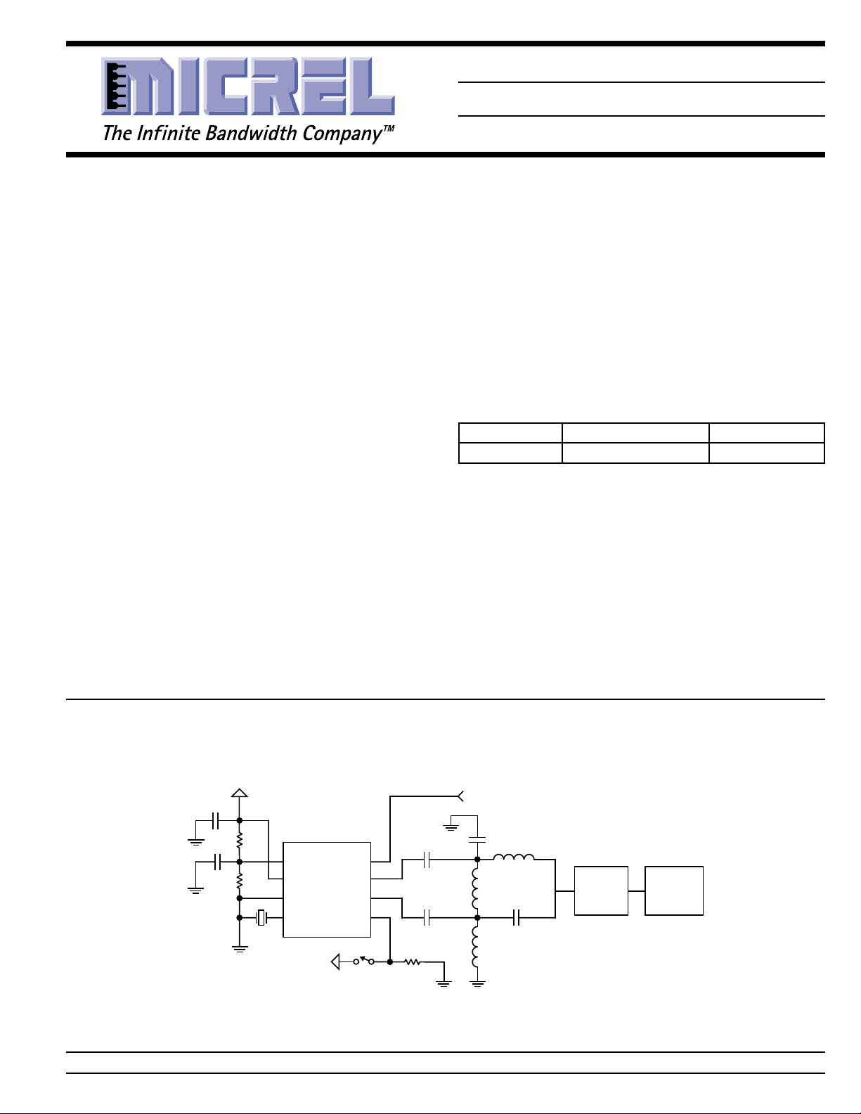
T ypical Application
+5V
ASK DATA INPUT
4.7µF
RP1
0.1µF
Note: Example for 868MHz
100k
RP2
6.8k
Y1
MICRF103
PC
VDD
VSS
REFOSC
+5V
ASK
ANTP
ANTM
STBY
8.2pF
100pF
100k
Figure 1
QwikRadio is a trademark of Micrel, Inc. The QwikRadio ICs were developed under a partnership agreement with AIT of Orlando, Florida.
Micrel, Inc. • 1849 Fortune Drive • San Jose, CA 95131 • USA • tel + 1 (408) 944-0800 • fax + 1 (408) 944-0970 • http://www.micrel.com
June 2002 1 MICRF103
1.0pF
10nH
27nH
27nH
1.0pF
SAW Filter
50Ω
Monopole
PCB Antenna
Page 2
MICRF103 Micrel
Pin Configuration
VDD
VSS
REFOSC
Pin Description
Pin Number Pin Name Pin Function
1 PC Power Control Input. The voltage at this pin should be set between 0.1V to
2 VDD Positive power supply input for the IC.
3 VSS This pin is the ground return for the IC. A power supply bypass capacitor
4 REFOSC This is the timing reference frequency which is the transmit frequency
5 STBY Input for transmitter stand-by control pin is pulled to VDD for transmit
6 ANTM Negative RF power output to drive one side of the transmit antenna.
7 ANTP Positive RF power output to drive the other side of the transmit antenna.
8 ASK Amplitude Shift Key modulation data input pin. For CW operation, connect
1PC
2
3
4
8 ASK
7
ANTP
ANTM
6
STBY
5
MICRF103BM
0.4V for normal operation.
connected from VDD to VSS should have the shortest possible path.
divided by 64. Connect a crystal (mode dependent) between this pin and
VSS, or drive the input with an AC coupled 0.5Vpp input clock. See
ence Oscillator
operation and VSS for stand-by mode.
this pin to VDD.
section in this data sheet under
Electrical Characteristics.
Refer-
MICRF103 2 June 2002
Page 3

MICRF103 Micrel
Absolute Maximum Ratings (Note 1)
Supply Voltage(V
Voltage on I/O Pins ............................. V
Storage Temperature Range ...................-65°C to + 150°C
Lead Temperature (soldering, 10 seconds) ........... + 300°C
ESD Rating, Note 3
) .....................................................+6V
DD
–0.3 to VDD+0.3
SS
Operating Ratings (Note 2)
Supply Voltage (V
Maximum Supply Ripple Voltage ...............................10mV
PC Input Range......................................0.1V < VPC < 0.4V
Ambient Operating Temperature (TA) ........ –40°C to +85°C
Programmable Transmitter Frequency Range:
) .................................... 4.75V to 5.5V
DD
........................................................ 800MHz to 1GHz
Electrical Characteristics
Specifications apply for 4.75V < VDD < 5.5V, VPC = 0.35V, TA = 25°C, freq
–40°C ≤ TA ≤ 85°C unless otherwise noted.
Parameter Condition Min Typ Max Units
Power Supply
Standby Supply Current, I
MARK Supply Current, I
SPACE Supply Current, I
MARK/SPACE Ratio 33%@868MHz 16 mA
RF Output Section and Modulation Limits:
Maximum Power Level, P
Output Power Variation over supply and temperature ±2 dBm
Extinction ratio for ASK 38 45 dBc
Varactor tuning range Note 5 2.6 3.0 3.3 pF
Reference Oscillator Section
Reference Oscillator Input 300 kΩ
Impedance
Reference Oscillator Source 5.0 µA
Current
Reference Oscillator Input 0.2 1.0 V
Voltage (peak-to-peak)
Digital / Control Section
Calibration Time note 7, ASK=HIGH 20 ms
Power Amplifier Output Hold-off note 4, STDBY transition from LOW to HIGH 5 ms
Time from STBY crystal, ESR < 20Ω
Transmitter Stabilization Time from external reference (500mVpp) 9 ms
From STBY crystal, ESR < 20Ω 12 ms
Maximum Data rate
- ASK modulation duty cycle of the modulating signal = 50% 115 kbits/s
STBY HIGH V
STBY LOW V
ASK Pin VIH, input high voltage 0.8V
ASK Input Current ASK = 0V, 5.0V input current –10 0.1 10 µA
Q
ON
OFF
OUT
V
< 0.5V 0.10 µA
STBY
@868MHz 19 26.5 mA
@915MHz 20 27.5 mA
@868MHz 14 18 mA
@915MHz 15 21 mA
33%@915MHz 17 mA
@868MHz (EIRP) -3 dBm
@915MHz (EIRP) -3 dBm
enable voltage 0.8V
IH
IL
VIL, input low voltage 0.1V
= 13.5625MHz, STBY = VDD. Bold values indicate
REFOSC
DD
DD
0.1V
DD
DD
PP
V
V
V
June 2002 3 MICRF103
Page 4

MICRF103 Micrel
Note 1. Exceeding the absolute maximum rating may damage the device.
Note 2. The device is not guaranteed to function outside its operating rating.
Note 3. Devices are ESD sensitive. Handling precautions recommended. Human body model, 1.5k in series with 100pF.
Note 4. After the release of the STDBY, the device requires an initialization time to settle the REFOSC and the internal PLL. The first MARK state
(ASK HIGH) after exit from STDBY needs to be longer than the initialization time. The subsequent low to high transitions will be treated as
data modulation whereby the envelope transition time will apply.
Note 5. The varactor capacitance tuning range indicates the allowable external antenna component variation to maintain tune over normal production
tolerances of external components. Guaranteed by design not tested in production.
Note 6. For the ASK modulation scheme, the part will accept ASK (digital ON/OFF) input and will transmit the data with a finite extinction ratio and the
pin will set the MARK power level.
Note 7. When the device is first powered up or it loses power momentarily, it goes into the calibration mode to tune up the transmit antenna.
Test Circuit
MICRF103
PC
VDD
VSS
REFOSC ASK
STBY
ANTP
ANTM
7.1nH
680pF
100Ω 4:1
200Ω
680pF
100Ω
50Ω
MICRF103 4 June 2002
Page 5

MICRF103 Micrel
Typical Characteristics
Mark Current
35
30
25
(mA)
20
ON
15
10
MARK I
vs. PC Voltage
5
0
0 0.1 0.2 0.3 0.4 0.5 0.6 0.7
VPC (V)
Output Power
vs. PC Pin Voltage
30
20
10
0
(dBm)
OUT
-10
-20
-30
MARK P
-40
-50
0 0.1 0.2 0.3 0.4 0.5 0.6 0.7
VPC (V)
June 2002 5 MICRF103
Page 6

MICRF103 Micrel
Functional Diagram
STBY
VDD
PC
REF.OSC
VDD
Reference
Oscillator (1)
Reference
Phase
Detector
Bias
(2)
(10)
TX
Bias
Control
Prescaler
÷64
(5)
(3)
VCO (4)
Figure 2. MICRF103 Block Diagram
(9)
Buffer
Buffer
(6a)
(6b)
Antenna
Tuning
Control
(7)
Power
Amp
(8)
Varactor
Device
(11)
ASK
ANTP
ANTM
VSS
Functional Description
The block diagram illustrates the basic structure of the
MICRF103. Identified in the figure are the principal functional
blocks of the IC, namely the (1, 2, 3, 4, 5) UHF synthesizer,
(6a/b) Buffer, (7) Antenna tuner, (8) Power amplifier, (9) TX
bias control, (10) Reference bias and (11) Process tuner.
The UHF synthesizer generates the carrier frequency with
quadrature outputs. The in-phase signal (I) is used to drive
the PA and the quadrature signal (Q) is used to compare the
antenna signal phase for antenna tuning purpose.
The antenna tuner block senses the phase of the transmit
signal at the antenna port and controls the varactor capacitor
to tune the antenna.
The power control unit senses the antenna signal and controls the PA bias current to regulate the antenna signal to the
transmit power.
MICRF103 6 June 2002
The process tune circuit generates process independent bias
currents for different blocks.
Included within the IC is a differential varactor that serves as
the tuning element to insure that the transmit frequency and
antenna are aligned with the receiver over all supply and
temperature variations.
Page 7

MICRF103 Micrel
Package Information
0.026 (0.65)
MAX)
PIN 1
0.154 (3.90)
0.050 (1.27)
0.057 (1.45)
0.049 (1.25)
TYP
0.016 (0.40)
TYP
0.197 (5.0)
0.189 (4.8)
0.063 (1.60) MAX
SEATING
PLANE
8-Pin SOP (M)
DIMENSIONS:
INCHES (MM)
0.193 (4.90)
0.244 (6.20)
0.228 (5.80)
45°
3°–6°
MICREL, INC. 1849 FORTUNE DRIVE SAN JOSE, CA 95131 USA
TEL + 1 (408) 944-0800 FAX + 1 (408) 944-0970 WEB http://www.micrel.com
This information is believed to be accurate and reliable, however no responsibility is assumed by Micrel for its use nor for any infringement of patents or
other rights of third parties resulting from its use. No license is granted by implication or otherwise under any patent or patent right of Micrel, Inc.
© 2002 Micrel, Incorporated
June 2002 7 MICRF103
 Loading...