

Page 1
MICRF011
QwikRadiotm Receiver/Data Demodulator
Preliminary Information
General Description
The MICRF011, an enhanced version of the MICRF001, is a single chip
OOK (ON-OFF Keyed) Receiver IC for remote wireless applications,
employing Micrel’s latest QwikRadiotm technology. This device is a true
“antenna-in, data-out” monolithic device. All RF and IF tuning is
accomplished automatically within the IC, which eliminates manual
tuning and reduces production costs. Receiver functions are completely
integrated. The result is a highly reliable yet extremely low cost solution
for high volume wireless applications. Because the MICRF011 is a true
single-chip radio receiver, it is extremely easy to apply, minimizing design
and production costs, and improving time to market.
The MICRF011 is a functional and pin equivalent upgrade to the
MICRF001, providing improved range, lower power consumption, and
higher data rate support when in FIXED mode.
The MICRF011 provides two fundamental modes of operation, FIXED
and SWP. In FIXED mode, the device functions like a conventional
superheterodyne receiver, with an (internal) local oscillator fixed at a
single frequency based on an external reference crystal or clock. As with
any conventional superheterodyne receiver, the transmit frequency must
be accurately controlled, generally with a crystal or SAW (Surface
Acoustic Wave) resonator.
In SWP mode, the MICRF011 sweeps the (internal) local oscillator at
rates greater than the baseband data rate. This effectively “broadens”
the RF bandwidth of the receiver to a value equivalent to conventional
super-regenerative receivers. Thus the MICRF011 can operate with less
expensive LC transmitters without additional components or tuning, even
though the receiver topology is still superheterodyne. In this mode the
reference crystal can be replaced with a less expensive ± 0.5% ceramic
resonator.
All post-detection (demodulator) data filtering is provided on the
MICRF011, so no external filters need to be designed. Any one of four
filter bandwidths may be selected externally by the user. Bandwidths
range in binary steps, from 0.625kHz to 5kHz (SWP mode) or 1.25kHz to
10kHz (FIXED mode). The user only needs to program the appropriate
filter selection based on data rate and code modulation format.
Features
• Complete UHF receiver on a monolithic chip
• Frequency range 300 to 440 MHz
• Typical range over 200 meters with monopole
antenna
• Data rates to 2.5kbps (SWP), 10kbps (FIXED)
• Automatic tuning, no manual adjustment
• No Filters or Inductors required
• Low Operating Supply Current—2.4 mA at 315MHz
• Fully pin compatible with MICRF001
• Very low RF re-radiation at the antenna
• Direct CMOS logic interface to standard decoder
and microprocessor ICs
• Extremely low external part count
Applications
• Garage Door/Gate Openers
• Security Systems
• Remote Fan/Light Control
IMPORTANT: Items in bold type represent changes from
the MICRF001 specification. Differences between the
MICRF001 and -011 are identified in table 2, together with
design considerations for using the -011 in present
MICRF001 designs.
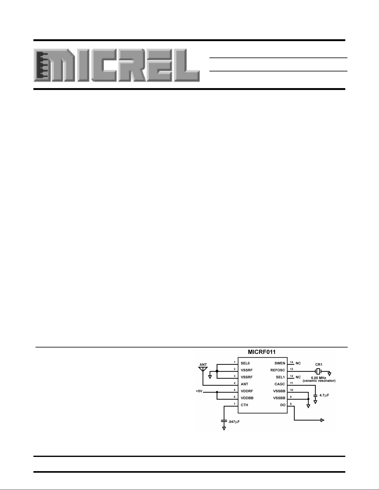
Typical Operating Circuit
385.5 MHz, 1200 bps OOK RECEIVER
Micrel Inc. • 1849 Fortune Drive San Jose, Ca 95131 • USA • tel + 1 (408) 944-0800 • fax + 1 (408) 944-0970 • http://www.micrel.com
Page 2
MICRF011 Micrel
QwikRadio
tm
Ordering Information
Part Number Temperature Range Package
MICRF011BN
MICRF011BM
-40°C to +85°C
-40°C to +85°C
14-Pin DIP
14-Pin SOIC
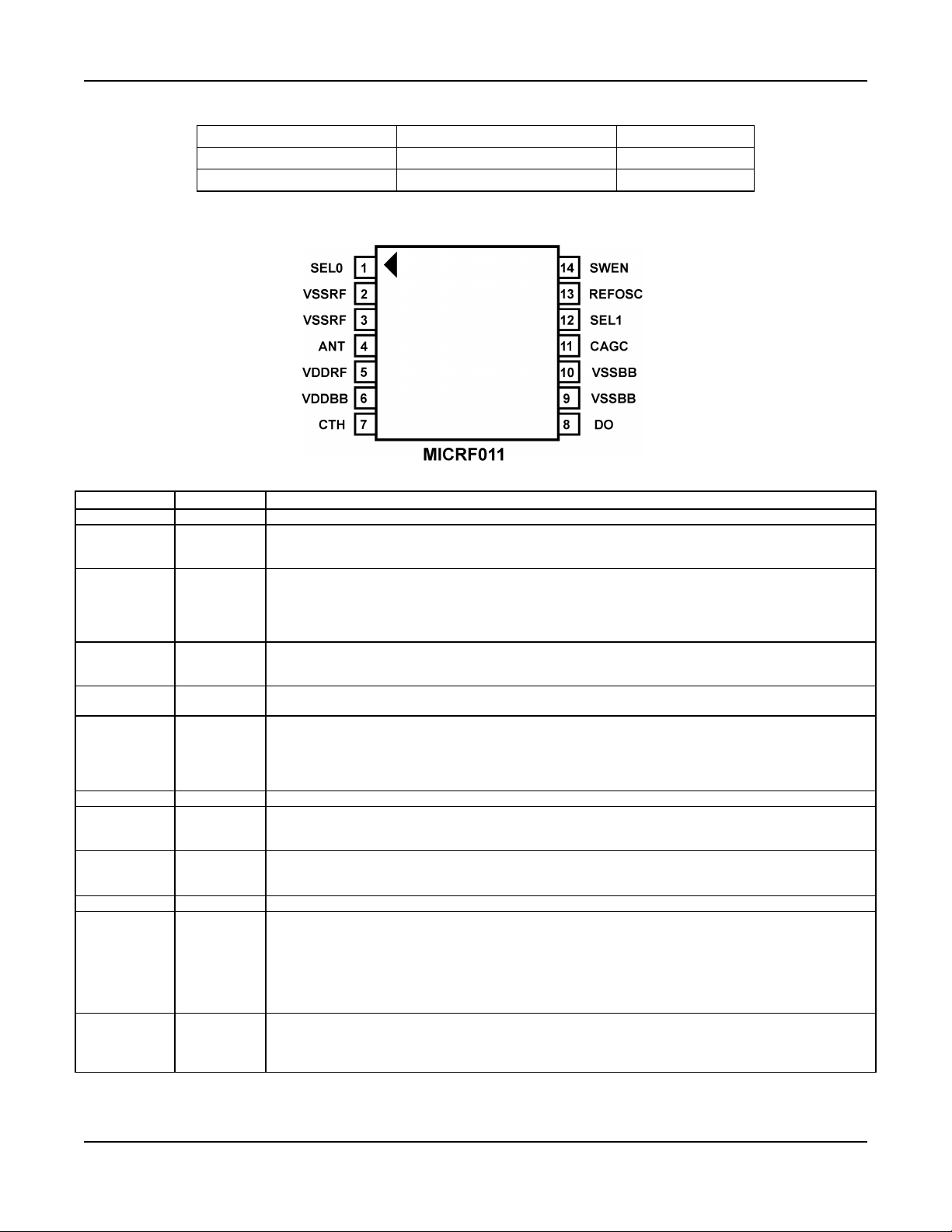
Pin Configuration (DIP and SOIC)
Pin Description
Pin Number Pin Name Pin Function
1 SEL0 Programs desired Demodulator Filter Bandwidth. This pin in internally pulled-up to VDD. See Table 1.
2/3 VSSRF This pin is the ground return for the RF section of the IC. The bypass capacitor connected from VDDRF to
4 ANT This is the receive RF input, internally ac-coupled. Connect this pin to the receive antenna. Input
5 VDDRF This pin is the positive supply input for the RF section of the IC. VDDBB and VDDRF should be connected
6 VDDBB This pin is the positive supply input for the baseband section of the IC. VDDBB and VDDRF should be
7 CTH This capacitor extracts the (DC) average value from the demodulated waveform, which becomes the
8 DO Output data pin. CMOS level compatible.
9/10 VSSBB This is the ground return for the baseband section of the IC. The bypass and output capacitors connected
11 CAGC Integrating capacitor for on-chip receive AGC (Automatic Gain Control). The Decay/Attack time-constant
12 SEL1 Programs desired Demodulator Filter Bandwidth. This pin in internally pulled-up to VDD. See Table 1.
13 REFOSC This is the timing reference for on-chip tuning and alignment. Connect either a ceramic resonator or crystal
VSSRF should have the shortest possible lead length. For best performance, connect VSSRF to VSSBB
at the power supply only (i.e., keep VSSBB currents from flowing through VSSRF return path).
impedance is high (FET gate) with approximately 2pF of shunt (parasitic) capacitance. For applications
located in high ambient noise environments, a fixed value band-pass network may be connected between
the ANT pin and VSSRF to provide additional receive selectivity and input overload protection. (See
“Application Note 22, MICRF001 Theory of Operation”.)
directly at the IC pins. Connect a low ESL, low ESR decoupling capacitor from this pin to VSSRF, as short
as possible.
connected directly at the IC pins.
reference for the internal data slicing comparator. Treat this as a low-pass RC filter with source impedance
of 118kohms (for REFOSC frequency ft=4.90MHz). Note that variation in source resistance with filter
selection no longer exists, as it does for the MICRF001. (See “Application Note 22, MICRF001 Theory
of Operation”, section 6.4). A standard ± 20% X7R ceramic capacitor is generally sufficient.
to VSSBB should have the shortest possible lead lengths. For best performance, connect VSSRF to
VSSBB at the power supply only (i.e., keep VSSBB currents from flowing through VSSRF return path).
(TC) ratio is nominally set as 10:1. Use of 0.47µF or greater is strongly recommended for best range
performance. See “Application Note 22, MICRF001 Theory of Operation” for further information.
(mode dependent) between this pin and VSSBB, or drive the input with an AC coupled 0.5Vpp input clock.
Use ceramic resonators without integral capacitors.
Note that if operated in FIXED mode, a crystal must be used; however in SWP mode, one may use either a
crystal or ceramic resonator. See “Application Note 22, MICRF001 Theory of Operation” for details on
14 SWEN This logic pin controls the operating mode of the MICRF011. When SWEN = HIGH, the MICRF011 is in
December 1998b MICRF011
frequency selection and accuracy.
SWP mode. This is the normal (default) mode of the device. When SWEN = LOW, the device operates
as a conventional single-conversion superheterodyne receiver. (See “Application Note 22, MICRF001
Theory of Operation” for details.) This pin is internally pulled-up to VDD.
2
Page 3

MICRF011 Micrel
SEL0 SEL1 Demodulator Bandwidth (Hz)
SWP Mode FIXED Mode
1 1
0 1
1 0
0 0
1250 2500
Nominal Demodulator (Baseband) Filter Bandwidth
QwikRadio
5000 10000
2500 5000
625 1250
Table 1
vs. SEL0, SEL1 and Mode
tm
No
.
1. Local Oscillator sweep range
reduced 2X. Affects SWP mode
only.
2. Local Oscillator sweep rate reduced
2X. Affects SWP mode only.
3. IF Center Frequency reduced 2X.
Affects both modes SWP and
FIXED.
4. IF Bandwidth reduced 2X. Affects
both modes SWP and FIXED.
5. FIXED mode Demod Filter cutoff
frequencies increased 2X. Affects
FIXED mode only.
6. CTH Pin Impedance
118kΩ @ ft=4.90 MHz [see Note 4].
Affects both modes SWP and
FIXED.
Design Change Retrofit Design Action
Reconsider Tx/Rx Frequency Alignment Error Budget, per App. Note 22.
If alignment tolerances cannot be met, consider:
(1) tighten ceramic resonator tolerance,
(2) replace ceramic resonator with crystal, or
(3) not to upgrade to -011
Impacts SWP mode maximum data rate.
If data rate constraint cannot be met, consider
(1) reduce system data rate by 2X, or
(2) not to upgrade to -011
Factor this change into Tx/Rx Frequency Alignment Error Budget.
FIXED mode users of -001 must change crystal frequency.
Factor this change into Tx/Rx Frequency Alignment Error Budget.
For FIXED mode only, choose next lower filter frequency (via control pins
SEL0/1), to maintain same range performance
Recompute appropriate value of CTH capacitor, and change value on PCB
Table 2
MICRF001/011 Change List and
Design Retrofit Guidelines
December 1998b MICRF011
3
Page 4
MICRF011 Micrel
QwikRadio
tm
ABSOLUTE MAXIMUM RATINGS
Supply Voltage (VDDRF, VDDBB).................................+7V
Voltage on any I/O Pin.........................VSS-0.3 to VDD+0.3
Junction Temperature..............................................+150°C
Storage Temperature Range.....................-65°C to + 150°C
Lead Temperature (soldering, 10 seconds).............+ 260°C
Operating Ratings
Supply Voltage (VDDRF, VDDBB)..................4.75V to 5.5V
Ambient Operating Temperature (TA)..........-40°C to +85°C
Package Thermal Resistance θJA (14 Pin DIP)........90°C/W
Package Thermal Resistance θJA (14 Pin SOIC)...120°C/W
This device is ESD sensitive: Meets Class 1ESD test
requirements (Human body Model, HBM), in
accordance with MIL-STD-883C, Method 3015. Do
not operate or store near strong electrostatic fields.
Use appropriate ESD precautions.
Electrical Characteristics
Unless otherwise stated, these specifications apply for Ta=-40°C to 85°C, 4.75<VDD<5.5V. All voltages are with respect to
Ground; Positive currents flow into device pins. CAGC = 4.7µF, CTH = .047µF, VDDRF= VDDBB = VDD. REFOSC
frequency =4.90MHz. Note: Items in bold represent changes from the MICRF001 specification.
Parameter Test Conditions MIN TYP MAX UNITS
Power Supply
Operating Current 2.4 mA
RF/IF Section
Receiver Sensitivity Note 1, 3 -103 dBm
IF Center Frequency Note 4
IF 3dB Bandwidth Note 3, 4
0.86
0.43
RF Input Range 300 440 MHz
Receive Modulation Duty-Cycle 20 80 %
Maximum Receiver Input
Spurious Reverse Isolation
Rsc = 50Ω
ANT pin, Rsc = 50Ω Note 2
-20 dBm
30
AGC Attack / Decay ratio T(Attack) / T(Decay) 0.1
Local Oscillator Stabilization Time To 1% of Final Value 2.5 msec
Demod Section
CTH Source Impedance Note 5
118k
CTH Source Impedance Variation -15 +15 %
Demod Filter Bandwidth SEL0 = SEL1 = SWEN = VDD, Note 4, 6 4160 Hz
Demod Filter Bandwidth SEL0 = SEL1 = VDD, SWEN = VSS
8320 Hz
Note 4, 6
Digital Section
REFOSC Input Impedance 200k
Input Pullup Current SEL0, SEL1, SWEN = VSS 8 µA
Input High Voltage SEL0, SEL1, SWEN 0.8VDD V
Input Low Voltage SEL0, SEL1, SWEN 0.2VDD V
Output Current DO pin, Push-Pull 10 µA
Output High Voltage DO pin, Iout = -1µA 0.9VDD V
Output Low Voltage DO pin, Iout = +1µA 0.1VDD V
Output Tr, Tf DO pin, Cload= 15pF 10 µsec
MHz
MHz
µVrms
Ω
Ω
Note 1: Sensitivity is defined as the average signal level measured at the input necessary to achieve 10e-2 Bit Error Rate (BER). The
Note 2: Spurious reverse isolation represents the spurious components which appear on the RF input (ANT) pin measured into 50Ω
Note 3: Sensitivity, a commonly specified Receiver parameter, provides an indication of the Receiver’s input referred noise, generally
December 1998b MICRF011
input signal is defined as a return-to-zero (RZ) waveform with 50% average duty cycle (e.g., Manchester Encoded Data) at a
data rate of 300bps. The RF input is assumed to be matched into 50Ω.
with an input RF matching network.
input thermal noise. However, it is possible for a more sensitive receiver to exhibit range performance no better than that of a
less sensitive receiver, if the “ether” noise is appreciably higher than the thermal noise. “Ether” noise refers to other interfering
“noise” sources, such as FM radio stations, pagers, etc.
A better indicator of receiver range performance is usually given by its Selectivity, often stated as Intermediate Frequency (IF)
or Radio Frequency (RF) bandwidth, depending on receiver topology. Selectivity is a measure of the rejection by the receiver
of “ether” noise. More selective receivers will almost invariably provide better range. Only when the receiver selectivity is so
high that most of the noise on the receiver input is actually thermal will the receiver demonstrate sensitivity-limited
performance.
4
Page 5

MICRF011 Micrel
(Temperature=25°°C, VDD=5.0V, SWP Mode)
QwikRadio
tm
Note 4: Parameter scales linearly with REFOSC frequency ft. For any REFOSC frequency other than 4.90MHz, compute new
parameter value as the ratio [(REFOSC FREQ (in MHz) / 4.90] * [Parameter Value @ 4.90MHz]. Example: For REFOSC
Freq. ft = 6.00MHz, [Parameter Value @ 6.00MHz] = (6.00 / 4.90) *[Parameter Value @ 4.90MHz].
Note 5: Parameter scales inversely with REFOSC frequency ft. For any REFOSC frequency other than 4.90MHz, compute new
parameter value as the ratio [4.90 / (REFOSC FREQ (in MHz)] * [Parameter Value @ 4.90MHz]. Example: For REFOSC
Freq. ft = 6.00MHz, [Parameter Value @ 6.00MHz] = (4.90 / 6.00) * [Parameter Value @ 4.90MHz].
Note 6: Demod filter bandwidths are related in a binary manner, so any of the (lower) nominal filter values may be derived simply by
dividing this parameter value by 2, 4, or 8 as desired.
Typical Performance Characteristics
MICRF011 IDD vs Frequency
6.10
5.60
5.10
IDD(mA)
4.60
4.10
3.60
IDD(mA)
3.10
2.60
2.10
1.60
250 275 300 325 350 375 400 425 450 475 500
Frequency (MHz)
MICRF011 IDD vs Temperature
(Frequency=315MHz, VDD=5.0V, SWP Mode)
3.30
3.10
2.90
2.70
2.50
2.30
2.10
1.90
December 1998b MICRF011
-40 -20 0 20 40 60 85
Temperature (C)
5
Page 6

MICRF011 Micrel
QwikRadio
tm
MICRF011 Block Diagram
December 1998b
66
MICRF011
Page 7

MICRF011 Micrel
QwikRadio
tm
Functional Description
Please refer to “MICRF011 Block Diagram”. Identified in the
figure are the three principal functional blocks of the IC,
namely (1) UHF Downconverter, (2) OOK Demodulator, and
(3) Reference and Control. Also shown in the figure are two
capacitors (CTH, CAGC) and one timing component (CR),
usually a ceramic resonator. With the exception of a supply
decoupling capacitor, these are all the external components
needed with the MICRF011 to construct a complete UHF
receiver. Three control inputs are shown in the block
diagram, SEL0, SEL1 and SWEN. Through these logic
inputs the user can control the operating mode and
programmable functions of the IC. These inputs are CMOS
compatible, and are pulled-up on the IC.
Input SWEN selects the operating mode of the IC (FIXED
mode or SWP mode). When low, the IC is in FIXED mode,
and functions as a conventional superheterodyne receiver.
When SWEN is high, the IC is in SWP mode. In this mode,
while the topology is still superheterodyne, the local
oscillator (LO) is deterministically swept over a range of
frequencies at rates greater than the data rate. When
coupled with a peak-detecting demodulator, this technique
effectively increases the RF bandwidth of the MICRF011, so
the device can operate in applications where significant
Transmitter/Receiver frequency misalignment may exist.
[Note: The swept LO technique does not affect the IF
bandwidth, so noise performance is not impacted relative to
FIXED mode. In other words, the IF bandwidth is the same
(500kHz) whether the device is in FIXED or SWP mode.]
Due to limitations imposed by the LO sweeping process, the
upper limit on data rate in SWP mode is approximately
2.5kbps. Data rates beyond 10kbps are possible in FIXED
mode however.
Examples of SWP mode operation include applications
which utilize low-cost LC-based transmitters, whose transmit
frequency may vary up to ± 0.5% over initial tolerance,
aging, and temperature. In this (patent-pending) mode, the
LO frequency is varied in a prescribed fashion which results
in downconversion of all signals in a band approximately
1.5% around the transmit frequency. So the Transmitter
may drift up to ± 0.5% without the need to retune the
Receiver, and without impacting system performance. Such
performance is not achieved with currently available crystalbased superheterodyne receivers, which can operate only
with SAW or crystal based transmitters.
[Note: In SWP mode only, a range penalty will occur in
installations where there exists a competing signal of
sufficient strength in this small frequency band of 1.5%
around the transmit frequency. This results from the fact
that sweeping the LO indiscriminately “sweeps” all signals
within the sweep range down into the IF band. This same
penalty also exists with super-regenerative type receivers,
as their RF bandwidth is also generally 1.5%. So any
application for a super-regenerative receiver is also an
application for the MICRF011 in SWP mode.]
For applications where the transmit frequency is accurately
set for other reasons (e.g., applications where a SAW
transmitter is used for its mechanical stability), the user may
choose to configure the MICRF011 as a standard
superheterodyne receiver (FIXED mode), mitigating the
aforementioned problem of a competing close-in signal.
This can be accomplished by tying SWEN to ground. Doing
so forces the on-chip LO frequency to a fixed value. In
FIXED mode, the ceramic resonator would be replaced with
a crystal. Generally, however, the MICRF011 can be
operated in SWP mode, using a ceramic resonator, with
either LC or CRYSTAL/SAW based transmitters, without
any significant range difference.
The inputs SEL0 and SEL1 control the Demodulator filter
bandwidth in four binary steps (625Hz-5000Hz in SWP,
1250Hz-10000Hz in FIXED mode), and the user must select
the bandwidth appropriate to his needs.
Rolloff response of the IF Filter is 5th order, while the
demodulator data filter exhibits a 2nd order response.
Multiplication factor between the REFOSC frequency ft and
the internal Local Oscillator (LO) is 64.5X for FIXED mode,
and 64.25X for SWP mode (i.e., for ft = 6.00MHz in FIXED
mode, LO frequency = 6.00MHz * 64.5 = 387MHz).
Slicing Level and the CTH Capacitor
Extraction of the DC value of the demodulated signal for
purposes of logic-level data slicing is accomplished by
external capacitor CTH and the on-chip switched-cap
“resistor” RSC, indicated in the block diagram. The effective
resistance of RSC is 118kohms. The value of capacitor
CTH is easily calculated, once the slicing level time-constant
is chosen. Values vary somewhat with decoder type, data
pattern, and data rate, but typical Slicing Level time
constants range 5-50msec. Optimization of the CTH value
is required to maximize range, as discussed in “Application
Note 22, MICRF001 Theory of Operation”, section 6.4.
During quiet periods (i.e., no signal transmissions) the Data
Output (DO pin) transitions randomly based on noise. This
may present problems for some decoders. The most
common solution is to introduce a small offset (“Squelch”)
on the CTH pin so that noise does not trigger the internal
comparator. Usually 20-30mV is sufficient, and may be
introduced by connecting a several-Megohm resistor from
the CTH pin to either VSS or VDD, depending on the desired
offset polarity. Since the MICRF011 is an AGC’d receiver,
noise at the internal comparator input is always the same,
set by the AGC. So the squelch offset requirement does not
change as the local “ether” noise changes from installation
to installation. Note that introducing squelch will reduce
range modestly, so only introduce an amount sufficient to
“quiet” the output.
AGC Function and the CAGC Capacitor
The signal path has automatic gain control (AGC) to
increase input dynamic range. An external capacitor,
CAGC, must be connected to the CAGC pin of the device.
The ratio of decay-to-attack time-constant is fixed at 10:1
(i.e., the attack time constant is 1/10th the decay time
constant), and this ratio cannot be changed by the user.
However, the attack time constant is selectable by the user
through the value of capacitor CAGC.
December 1998b
77
MICRF011
Page 8

MICRF011 Micrel
QwikRadio
tm
[By adding resistance from the CAGC pin to VDDBB or
VSSBB in parallel with the CAGC capacitor, the ratio of
decay-to-attack time-constant may be varied, although the
value of such adjustments must be studied on a perapplication basis. Generally the design value of 10:1 is
adequate for the vast majority of applications.] See
“Application Note 22”.
To maximize system range, it is important to keep the AGC
control voltage ripple low, preferably under 10mVpp once
the control voltage has attained its quiescent value. For this
reason capacitor values ≥ 0.47uF are recommended.
Reference Oscillator (REFOSC) and External Timing
Element
All timing and tuning operations on the MICRF011 are
derived from the REFOSC function. This function is a
single-pin Colpitts-type oscillator. The user may handle this
pin in one of three possible ways:
(1) connect a ceramic resonator, or
(2) connect a crystal, or
(3) drive this pin with an external timing signal.
The third approach is attractive for further lowering system
cost if an accurate reference signal exists elsewhere in the
system (e.g., a reference clock from a crystal or ceramic
resonator-based microprocessor). An externally applied
signal should be AC-coupled, and resistively-divided down
(or otherwise limited) to approximately 0.5Vpp. The specific
reference frequency required is related to the system
transmit frequency, and the operating mode of the device as
set by the SWEN control pin. See “Application Note 22,
MICRF001 Theory of Operation” for a discussion of
frequency selection and accuracy requirements.
MICRF011 Frequency and Capacitor Selection
Here ft is in MHz. Connect a crystal of frequency ft to the
REFOSC pin of the MICRF011. 4 decimal-place accuracy
on the frequency is generally adequate. The following table
identifies ft for some common Transmit frequencies when
the MICRF011 is operated in FIXED mode.
Transmit Freq. ftx (MHz) REFOSC Freq. ft (MHz)
315
418
433.92
2. Selecting REFOSC Frequency ft (SWP Mode)
Selection of REFOSC frequency ft in SWP mode is much
simpler than in FIXED mode, due to the LO sweeping
process. Further, accuracy requirements of the frequency
reference component are significantly relaxed.
In SWP mode, ft is given by equation (3):
ft = ftx / 64.25. (3)
Connect a ceramic resonator of frequency ft to the REFOSC
pin of the MICRF011. 2-decimal place accuracy is generally
adequate. (A crystal may also be used if desired, but may
be necessary to reduce the Rx frequency ambiguity if the Tx
frequency ambiguity is excessive. See Application Note 22
for further details.)
3. Selecting Capacitor CTH
First step in the process is selection of a Data Slicing Level
timeconstant. This selection is strongly dependent on
system issues, like system decode response time and data
code structure (e.g., existence of data preamble, etc.). This
issue is too broad to discuss here, and the interested reader
should consult the Application Note 22.
4.8970
6.4983
6.7458
Selection of the REFOSC frequency ft, Slicing Level (CTH)
capacitor, and AGC capacitor are briefly summarized in this
section. Please see Application Note 22 for complete
details.
1. Selecting REFOSC Frequency ft (FIXED Mode)
As with any superheterodyne receiver, the difference
between the (internal) Local Oscillator (LO) frequency flo
and the incoming Transmit frequency ftx must ideally equal
the IF Center frequency. Equation (1) may be used to
compute the appropriate flo for a given ftx:
flo = ftx ± 1.064 * (ftx / 390) (1)
where ftx and flo are in MHz. Note that two values of flo
exist for any given ftx, distinguished as “high-side mixing”
and “low-side mixing”, and there is generally no preference
of one over the other.
After choosing one of the two acceptable values of flo, use
equation (2) to compute the REFOSC frequency ft:
ft = flo / 64.5. (2)
December 1998b
Source impedance of the CTH pin is given by equation (4),
where ft is in MHz:
Rsc = 118kΩ * (4.90 / ft). (4)
Assuming that a Slicing Level Timeconstant TC has been
established, capacitor CTH may be computed using
equation (5):
CTH = TC / Rsc. (5)
88
MICRF011
Page 9

MICRF011 Micrel
QwikRadio
tm
3. Selecting CAGC Capacitor
Selection of CAGC is dictated by minimizing the ripple on
the AGC control voltage, by using a sufficiently large
capacitor. It is Micrel’s experience that CAGC should be in
the vicinity of 0.47µF to 4.7µF. Large capacitor values
should be carefully considered, as this determines the time
required for the AGC control voltage to settle from a
completely discharged condition. AGC settling time from a
completely discharged (0-volt) state is given approximately
by equation (6):
∆T = (1.333 * CAGC) – 0.44 (6)
where CAGC is in microfarads, and ∆T is in seconds.
I/O Pin Interface Circuitry
Interface circuitry for the various I/O pins of the MICRF011 is
shown in Figures 1 through 6. Specific information
regarding each of these circuits is discussed in the following
sub-paragraphs. Not shown are ESD protection diodes
which are applied to all input and output pins.
1. ANT Pin
The ANT pin is internally AC-coupled via a 3pF capacitor, to
capacitor CAGC. The attack current is nominally 15µA,
while the decay current is a 1/10th scaling of this,
approximately 1.5µA. Signal gain of the RF/IF strip inside
the IC diminishes as the voltage on CAGC decreases. By
simply adding a capacitor to CAGC pin, the attack/decay
time constant ratio is fixed at 1:10. Further discussion on
setting the attack time constant is found in “Application Note
22, MICRF001 Theory of Operation”, section 6.5.
Modification of the attack/decay ratio is possible by adding
resistance from CAGC pin either to VDDBB or VSSBB, as
desired.
4. DO Pin
The output stage for the Data Comparator (DO pin) is shown
in Figure 4. The output is a 10µA push-10µA pull, switched
current stage. Such an output stage is capable of driving
CMOS-type loads. An external buffer-driver is
recommended for driving high capacitance loads.
5. REFOSC Pin
The REFOSC input circuit is shown in Figure 5. Input
impedance is quite high (200kΩ). This is a Colpitts
oscillator, with internal 30pF capacitors. This input is
intended to work with standard ceramic resonators,
connected from this pin to VSSBB, although a crystal may
be used instead, where greater frequency accuracy is
required. The resonators should not contain integral
capacitors, since these capacitors are contained inside the
IC. Externally applied signals should be AC-coupled,
amplitude limited to approximately 0.5Vpp. The nominal DC
bias voltage on this pin is 1.4V.
Figure 1 ANT Pin
an RF N-channel MOSFET, as shown in Figure 1.
Impedance on this pin to VSS is quite high at low
frequencies, and decreases as frequency increases. In the
UHF frequency range, the device input can be modeled as
6.3kΩ in parallel with 2pF (pin capacitance) shunt to
VSSRF.
2. CTH Pin
Figure 2 illustrates the CTH pin interface circuit. CTH pin is
driven from a P-channel MOSFET source-follower biased
with approximately 10µA of bias current. Transmission
gates TG1 and TG2 isolate the 6.9pF capacitor. Internal
control signals PHI1/PHI2 are related in a manner such that
the impedance across the transmission gates looks like a
“resistance” of approximately 118kΩ. The DC potential on
the CTH pin is approximately 1.6V.
3. CAGC Pin
Figure 3 illustrates the CAGC pin interface circuit. The AGC
control voltage is developed as an integrated current into a
6. Control Inputs (SEL0, SEL1, SWEN)
Control input circuitry is shown in Figure 6. The standard
input is a logic inverter constructed with minimum geometry
MOSFETs (Q2, Q3). P-channel MOSFET Q1 is a large
channel length device which functions essentially as a
“weak” pullup to VDDBB. Typical pullup current is 5µA,
leading to an impedance to the VDDBB supply of typically
1MΩ.
December 1998b
99
MICRF011
Page 10

MICRF011 Micrel
QwikRadio
tm
Figure 2 CTH Pin
Figure 3 CAGC Pin
Figure 4 DO Pin
December 1998b
Figure 5 REFOSC Pin
1010
Figure 6 SEL0, SEL1, SWEN
MICRF011
Page 11

MICRF011 Micrel
QwikRadio
tm
Typical Application
The Figure below illustrates a typical application for the MICRF011 UHF Receiver IC. Operation in this example is at
385.5MHz, and may be customized by selection of the appropriate reference frequency (CR1), and adjustment of the antenna
length. The value of C4 would also change, if the optional input filter is used. Changes from the 1kbps data rate may require
a change in the value of R1. The Bill of Materials is shown in the accompanying chart.
Typical MICRF011 Application
385.5 MHz Operating Frequency
1kbps Operation
6-Bit Address Decode
Bill of Materials
Item Part Number Manufacturer Description
U1 MICRF011 Micrel UHF Receiver
U2 HT-12D Holtek Logic decoder
CR1 CSA6.00MG Murata 6.00MHz Cer. Res.
D1 SSF-LX100LID Lumex RED LED
R1 Bourns 68k, 1/4W ,5%
R2 Bourns 1k,1/4W, 5%
C1 Panasonic 4.7µF, Dip Tant. Cap
C3 Panasonic 0.47µF, Dip Tant. Cap
C2 Panasonic 2.2µF, Dip Tant. Cap
C4 Panasonic 8.2pF, COG Cer. Cap
Vendor Telephone Fax
Bourns (909) 781-5500 (909) 781-5273
Holtek (408) 894-9046 (408) 894-0838
Lumex (800) 278-5666 (847) 359-8904
Murata (800) 241-6574 (770) 436-3030
Panasonic (201) 348-7000 (201) 348-8164
MICREL INC. 1849 FORTUNE DRIVE SAN JOSE, CA 95131 USA
This information is believed to be accurate and reliable, however no responsibility is assumed by Micrel for its use nor for any infringement of patents or other rights
of third parties resulting from its use. No license is granted by implication or otherwise under any patent or patent right of Micrel Inc. This is preliminary
information and a final specification has not been completed. Before making any final design determination, consult with Micrel for final specifications.
December 1998b MICRF011
TEL + 1 (408) 944-0800 FAX + 1 (408) 944-0970 WEB http://www.micrel.com
©1998 Micrel Incorporated
11
 Loading...