

Page 1
MICRF004/RF044 Micrel
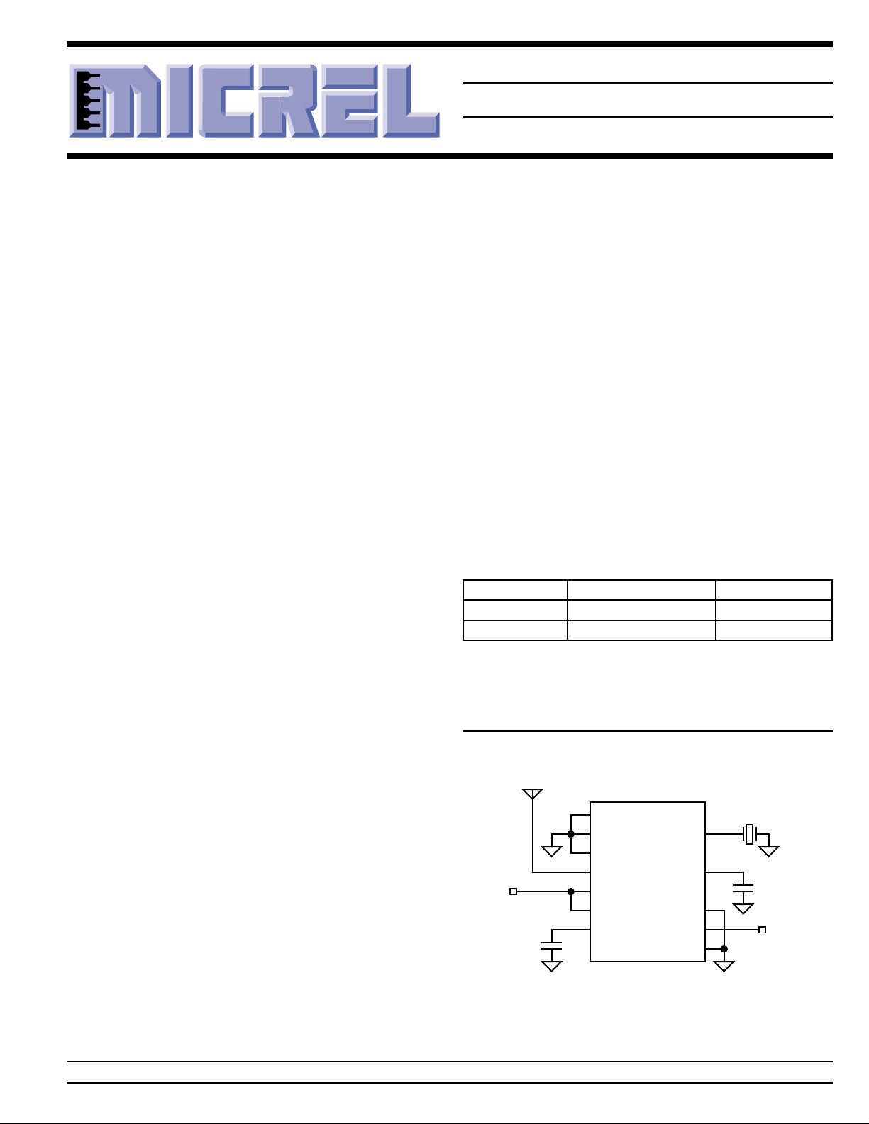
SEL0SEL0 SWEN
VSSRF REFOSC
VSSRF SEL1
ANT CAGC
VDDRF
WAKEB
VDDBB
SHUT
CTH DO
NC VSSBB
0.047µF
4.85MHz
(ceramic resonator)
Data
Output
MICRF004
4.7µF
+5V
MICRF004
QwikRadio™ Low-Power VHF Receiver
Advance Information
General Description
The MICRF004 QwikRadio™ VHF receiver is a single-chip
OOK (on-off keyed) receiver IC for remote wireless applications. This device is a true single-chip, “antenna-in, data-out”
device. All RF and IF tuning is accomplished automatically
within the IC which eliminates manual tuning production
costs and results in a highly reliable, extremely low-cost
solution for high-volume wireless applications.
The MICRF004 is extremely easy to apply, minimizing design
and production costs, and improving time to market. The
MICRF004 provides two fundamental modes of operation,
fixed and sweep.
In fixed mode, the device functions as a conventional superheterodyne receiver with an internal local oscillator operating
at a single frequency based on an external reference crystal
or clock. Fixed mode is for use with accurately-controlled
transmitters utilizing crystal or SAW (surface acoustic wave)
resonators.
In sweep mode, the MICRF004 sweeps the internal local
oscillator at rates greater than the baseband data rate. This
effectively broadens the RF bandwidth of the receiver to a
value equivalent to conventional superregenerative receivers. This allows the MICRF004 to operate with less expensive
LC transmitters without additional components or tuning,
even though the receiver topology is still superheterodyne. In
this mode the reference crystal can be replaced with a less
expensive ±0.5% ceramic resonator.
The MICRF004 features a shutdown control, which may be
used for duty-cycled operation, and a wake-up output, which
provides a logical indication of an incoming RF signal. These
features make the MICRF004 ideal for low- and ultra-lowpower applications, such as RKE (remote keyless entry) and
RFID (RF identification).
Since all post-detection (demodulator) data filtering is provided on the MICRF004, no external filters are required. One
of the four internal filter bandwidths must be externally
selected based on data rate and code modulation format.
Bandwidths range in binary steps, from 0.55kHz to 4.4kHz
(sweep mode) or 1.1kHz to 8.8kHz (fixed mode).
Features
• Complete VHF receiver on a monolithic chip
• 140MHz to 200MHz frequency range
• >200 meters typical range with monopole antenna
• 2.5kb/s sweep- and 10kb/s fixed-mode data rates
• Automatic tuning, no manual adjustment
• No filters or inductors required
• Low 240µA operating supply current at 150MHz
(10:1 duty cycle)
• Shutdown mode for >100:1 duty-cycle operation
• Wakeup for enabling decoders and microprocessors
• Very low RF antenna reradiation
• CMOS logic interface for standard ICs
• Extremely low external part count
Applications
• Automotive remote keyless entry
• Long range RF identification
• Remote fan and light control
• Garage door and gate openers
Ordering Information
Part Number Junction Temp. Range Package
MICRF004BM –40°C to +85°C 16-Lead SOP
MICRF004BN –40°C to +85°C 16-Pin DIP
8-pin versions available. See “Custom 8-Pin Options,” following page.
T ypical Application
QwikRadio is a trademark of Micrel, Inc.
February 9, 2000 1 MICRF004/RF044
Micrel, Inc. • 1849 Fortune Drive • San Jose, CA 95131 • USA • tel + 1 (408) 944-0800 • fax + 1 (408) 944-0970 • http://www.micrel.com
150MHz 1200b/s On-Off Keyed Receiver
Page 2
MICRF004/RF044 Micrel
Pin Configuration
VSSRF
VSSRF
ANT
VDDRF
VDDBB
CTH
NC
1SEL0
2
3
4
5
6
7
8
16 SWEN
REFOSC
15
SEL1
14
CAGC
13
WAKEB
12
SHUT
11
DO
10
VSSBB
9
16-Pin DIP (N) or SOP (M) Packages
MICRF004 2 February 9, 2000
Page 3

MICRF004/RF044 Micrel
Pin Description
Pin Number Pin Number Pin Name Pin Function
16-Pin Pkg. 8-Pin Pkg.
1 SEL0 Bandwidth Selection Bit 0 (Input): Configure with SEL1 to set the desired
demodulator filter bandwidth. See Table 1. Internally pulled-up to VDDRF.
2, 3 1 VSSRF RF [Analog] Return (Input): Ground return to the RF section power supply.
See “Application Information” for bypass capacitor details.
4 2 ANT Antenna (Input): High-impedance, internally ac coupled receiver input.
Connect this pin to the receive antenna. This FET gate input has approximately 2pF of shunt (parasitic) capacitance. See “Applications Information”
for optional band-pass filter information.
5 3 VDDRF RF [Analog] Supply (Input): Positive supply input for the RF section of the
IC. VDDBB and VDDRF should be connected together directly at the IC
pins. Connect a low ESL, low ESR decoupling capacitor from this pin to
VSSRF, as short as possible.
6 VDDBB Base-Band [Digital] Supply (Input): Positive supply input for the baseband
section of the IC. VDDBB and VDDRF should be connected together at the
IC pins.
7 4 CTH [Data Slicing] Threshold Capacitor (External Component): Capacitor
extracts the dc average value from the demodulated waveform which
becomes the reference for the internal data slicing comparator. See “Appli-
cations Information” for selection.
8 NC not internally connected
9 VSSBB Base-Band [Digital] Return (Input): Ground return to the baseband section
power supply. See “Application Information” for bypass capacitor and layout
details.
10 5 DO Digital Output (Output): CMOS-level compatible data output signal.
11 6 SHUT Shutdown (Input): Shutdown-mode logic-level control input. Pull low to
enable the receiver. This input has an internal pulled-up to VDDRF.
12 WAKEB Wakeup (Output): Active-low output that indicates detection of an incoming
RF signal. Signal is determined by monitoring for data preamble. CMOS-
level compatible.
13 7 CAGC AGC Capacitor (External Component): Integrating capacitor for on-chip
AGC (automatic gain control). The decay/attack time-constant (τ) ratio is
nominally 10:1. See “Applications Information” for capacitor selection.
14 SEL1 Bandwidth Selection Bit 1 (Input): Configure with SEL0, programs to set the
desired demodulator filter bandwidth. See Table 1. Internally pulled-up to
VDDRF.
15 8 REFOSC Reference Oscillator (External Component or Input): Timing reference for
on-chip tuning and alignment. Connect either a ceramic resonator or crystal
(mode dependent, see “Application Information”). between this pin and
VSSBB, or drive the input with an ac-coupled 0.5Vpp input clock.
16 SWEN Sweep-Mode Enable (Input): Sweep- or fixed-mode operation control input.
When VSWEN is high, the MICRF004 is in sweep mode; when SWEN is
low, the receiver operates as a conventional single-conversion superhetero-
dyne receiver. This pin is internally pulled-up to VDDRF.
February 9, 2000 3 MICRF004/RF044
Page 4
MICRF004/RF044 Micrel
Absolute Maximum Ratings (Note 1)
Supply Voltage (V
Reference Oscillator Input Voltage (V
Input/Output Voltage (V
Junction Temperature (TJ) ......................................+150°C
Storage Temperature Range (T
DDRF
, V
I/O
)....................................+7V
DDBB
REFOSC
)..........V
) ................. VSS–0.3 to VDD+0.3
)............ –65°C to +150°C
S
DDBB
Operating Ratings (Note 2)
Supply Voltage (V
Ambient Temperature (T
Package Thermal Resistance (θ
16-pin DIP (θJA)...................................................90°C/W
16-pin SOIC (θJA)..............................................120°C/W
DDRF
, V
)................ +4.75V to +5.5V
DDBB
)......................... –40°C to +85°C
A
)
JA
Lead Temperature (soldering, 10 sec.) ................... +260°C
ESD Rating, Note 3
Electrical Characteristics
V
= V
DDRF
values indicate –40°C ≤ TA ≤ +85°C; current flow into device pins is positive; unless noted.
Symbol Parameter Condition Min Typ Max Units
I
OP
I
STBY
RF Section, IF Section
f
IF
f
BW
f
ANT
Z
IN(ant)
Reference Oscillator
Z
REFOSC
I
REFOSC
Demodulator
Z
CTH
∆Z
CTH
I
ZCTH(leak)
= VDD where +4.75V ≤ VDD ≤ 5.5V, VSS = 0V; C
DDBB
= 4.7µF, CTH = 0.047µF; f
AGC
REFOSC
= 4.65MHz; TA = 25°C, bold
Operating Current continuous operation 2.4 mA
10:1 duty cycle 240 µA
Standby Current V
SHUT
= V
DD
0.35 µA
Receiver Sensitivity Notes 4, 6 –80 dBm
IF Center Frequency Note 7 0.86 MHz
IF 3dB Bandwidth Notes 6, 7 0.43 MHz
RF Input Range 145 200 MHz
Antenna Input Impdeance fIN = 150MHz 422 Ω
Receive Modulation Duty-Cycle 20 80 %
Maximum Receiver Input RSC = 50Ω –20 dBm
Spurious Reverse Isolation ANT pin, RSC = 50Ω, Note 5 30 µVrms
AGC Attack to Decay Ratio t
ATTACK
÷ t
DECAY
0.1
AGC Leakage Current TA = +85°C ±200 nA
Reference Oscillator extermal reference (250mV peak) 6 ms
Stabilization Time
ceramic resonator 5 ms
crystal 10 ms
Reference Oscillator 290 kΩ
Input Impedance
Reference Oscillator Note 10 0.1 2 Vp-p
Input Sensitivity
Reference Oscillator Current 4.5 µA
CTH Source Impedance Note 8 124 kΩ
CTH Source Impedance Variation ±15 %
CTH Leakage Current TA = +85°C ±200 nA
Demodulator Filter Bandwidth V
Demodulator Filter Bandwidth V
SEL0
SEL0
= V
= V
SEL1
SEL1
= V
SWEN
= VDD, V
= VDD, Notes 7, 9 3960 Hz
= VSS, 7930 Hz
SWEN
Note 7, 9
MICRF004 4 February 9, 2000
Page 5
MICRF004/RF044 Micrel
Symbol Parameter Condition Min Typ Max Units
Digital/Control Section
I
IN(pu)
V
IN(high)
V
IN(low)
I
OUT
V
OUT(high)
V
OUT(low)
tR, t
F
t
WAKEB
Note 1. Exceeding the absolute maximum rating may damage the device.
Note 2. The device is not guaranteed to function outside its operating rating.
Note 3. Devices are ESD sensitive. Use appropriate ESD precautions. Meets class 1 ESD test requirements, (human body model HBM), in accor-
Note 4: Sensitivity is defined as the average signal level measured at the input necessary to achieve 10
Note 5: Spurious reverse isolation represents the spurious components which appear on the RF input pin (ANT) measured into 50Ω with an input RF
Note 6: Sensitivity, a commonly specified receiver parameter, provides an indication of the receiver’s input referred noise, generally input thermal
Note 7: Parameter scales linearly with reference oscillator frequency fT. For any reference oscillator frequency other than 4.65MHz, compute new
Note 8: Parameter scales inversely with reference oscillator frequency fT. For any reference oscillator frequency other than 4.65MHz, compute new
Note 9: Demodulator filter bandwidths are related in a binary manner, so any of the (lower) nominal filter values may be derived simply by dividing this
Note 10: External signal generator used. When a crystal or ceramic resonator is used, the minimum voltage is 300mVp-p. The reference oscillator
Input Pull up Current SEL0, SEL1, SWEN, V
Input High Voltage SEL0, SEL1, SWEN 0.8V
Input Low Voltage SEL0, SEL1, SWEN 0.2V
SHUT
= V
SS
8 µA
DD
DD
V
V
Output Current DO, WAKEB pins, push-pull 10 µA
Output High Voltage DO, WAKEB pins, I
Output Low Voltage DO, WAKEB pins, I
Output Rise and Fall Times DO, WAKEB pins, C
= –1µA 0.9V
OUT
= +1µA 0.1V
OUT
= 15pF 10 µs
LOAD
DD
DD
V
V
Wakeup Output Time RFIN = TBDdBm, 4 ms
V
= V
SEL0
dance with MIL-STD-883C, method 3015. Do not operate or store near strong electrostatic fields.
defined as a return-to-zero (RZ) waveform with 50% average duty cycle (Manchester encoded data) at a data rate of 300b/s. The RF input is
assumed to be matched into 50Ω.
matching network.
noise. However, it is possible for a more sensitive receiver to exhibit range performance no better than that of a less sensitive receiver if the
background noise is appreciably higher than the thermal noise. Background noise refers to other interfering signals, such as FM radio
stations, pagers, etc.
A better indicator of achievable receiver range performance is usually given by its selectivity, often stated as fntermediate frequency (IF) or
radio frequency (RF) bandwidth, depending on receiver topology. Selectivity is a measure of the rejection by the receiver of “ether” noise.
More selective receivers will almost invariably provide better range. Only when the receiver selectivity is so high that most of the noise on the
receiver input is actually thermal will the receiver demonstrate sensitivity-limited performance.
parameter value as the ratio:
f MHz
REFOSC
Example: For reference oscillator freqency fT = 6.00MHz:
parameter value as the ratio:
Example: For reference oscillator frequency fT = 6.00MHz:
parameter value by 2, 4, or 8 as desired.
voltage amplitude is a function of the quality of the ceramic or crystal resonator.
4.65
(parameter value at 6.00MHz)
4.65
f MHz
REFOSC
(parmeter value at 4.65MHz)
(parameter value at 4.65MHz)
×
6.00
(paramter value at 4.65MHz)=×
4.65
×
(parmeter value at 4.65MHz)
4.65
(parmeter value at 4.65MHz)=×
6.00
SEL1
= V
SWEN
= V
SHUT
= V
SS
-2
BER (bit error rate). The input signal is
February 9, 2000 5 MICRF004/RF044
Page 6

MICRF004/RF044 Micrel
T ypical Characteristics
4
TA = 25°C
= 5V
V
DD
3
2
CURRENT (mA)
1
0
100 125 150 175 200 225 250
Functional Characteristics
Supply Current
vs. Frequency
Sweep Mode,
Continuous Operation
FREQUENCY (MHz)
Supply Current
vs. Temperature
4
f = 150MHz
V
= 5V
DD
3
2
CURRENT (mA)
1
0
-40 -20 0 20 40 60 80 100
TEMPERATURE (°C)
Sweep Mode,
Continuous Operation
Antenna Impedance
ycneuqerF
zHM04141.13.4j–35.21Fp36.2
zHM94178.604j–6.51Fp36.2
zHM06187.773j–81.51Fp36.2
zHM07163.553j–93.41Fp36.2
zHM37142.743j–15.31Fp46.2
zHM08189.333j–97.41Fp46.2
zHM48101.723j–74.31Fp56.2
zHM09134.613j–51.11Fp56.2
xelpmoC
ecnadepmI
ecnaticapaC
MICRF004 6 February 9, 2000
Page 7

MICRF004/RF044 Micrel
Functional Diagram
CAGC
C
AGC
SWEN
REFOSC
CR
Ceramic
Resonator
ANT
VDD
VSS
SEL0
SEL1
SHUT
RF
Amp
MICRF004
f
f
RX
IF
f
LO
Programmable
Synthesizer
Control
Logic
Reference
Oscillator
IF
Amp
5th Order
Band-Pass Filter
500kHz
VHF Downconverter
Functional Description
Refer to “MICRF004 Block Diagram”. Identified in the block
diagram are the four sections of the IC: UHF Downconverter,
OOK Demodulator, Reference and Control, and Wakeup.
Also shown in the figure are two capacitors (CTH, C
one timing component (CR), usually a ceramic resonator.
With the exception of a supply decoupling capacitor, these
are the only external components needed by the MICRF004
to assemble a complete UHF receiver. Four control inputs are
shown in the block diagram: SEL0, SEL1, SWEN, and SHUT.
Using these logic inputs, the user can control the operating
mode and selectable features of the IC. These inputs are
CMOS compatible, and are pulled-up on the IC.
Sweep-Mode Enable
Logic-input SWEN selects either fixed-mode or sweep-mode
operation. When SWEN is low, the IC is in fixed mode, and
functions as a conventional superheterodyne receiver. When
SWEN is high, the IC is in sweep mode.
Fixed-Mode Operation
For applications where the transmit frequency must be accurately set (that is, applications where a SAW transmitter is
used for its mechanical stability), the MICRF004 may be
configured as a standard superheterodyne receiver (fixed
mode). Fixed-mode operation receives a narrower bandwidth making it less susceptable to competing signals. Fixed
mode is selected by connecting SWEN to ground which
forces the on-chip LO frequency to a fixed value. In fixed
mode a crystal (higher frequency tolerance) must be used
instead of a ceramic resonator (lower frequency tolerance).
Data rates beyond 10kb/s are possible in fixed mode.
AGC
) and
AGC
IF
Amp
Control
Peak
Detector
2nd Order
Programmable
Low-Pass Filter
SwitchedCapacitor
Resistor
Resettable
Counter
WakeupReference and Control
R
OOK Demodulator
Compa-
SC
rator
DO
CTH
WAKEB
Sweep-Mode Operation
In sweep mode, while the topology is still superheterodyne,
the LO (local oscillator) is deterministically swept over a
range of frequencies at rates greater than the data rate. When
coupled with a peak-detecting demodulator, this technique
effectively increases the RF bandwidth of the MICRF004,
allowing the device to operate in applications where significant transmitter-receiver frequency misalignment may exist.
The swept-LO technique does not affect the IF bandwidth,
therefore noise performance is not degraded relative to fixed
mode. The IF bandwidth is 500kHz whether the device is
operating in fixed or sweep mode.
Due to limitations imposed by the LO sweeping process, the
upper limit on data rate in sweep mode is approximately
2.5kb/s.
Examples of sweep-mode operation include applications
utilizing low-cost LC-based transmitters, where the transmit
frequency may vary up to ±0.5% over initial tolerance, aging,
and temperature. In sweep mode, the LO frequency is varied
in a defined fashion which results in downconversion of all
signals in a band approximately 1.5% around the nominal
transmit frequency. The transmitter may drift up to ±0.5%
without the need to retune the receiver and without impacting
system performance. Similar performance is not currently
available with crystal-based superheterodyne receivers which
can operate only with SAW- or crystal-based transmitters.
In sweep mode only, a range reduction will occur in installations where there is an undesired competing signal of sufficient strength within of 2% to 3% around the transmit frequency. This is because the process indiscriminately in-
C
TH
February 9, 2000 7 MICRF004/RF044
Page 8

MICRF004/RF044 Micrel
cludes all signals within the sweep range. This same range
reduction also occurs with superregenerative receivers as
their RF bandwidth is also generally 2% to 3% around the
nominal transmit frequency. Any superregenerative receiver
application can instead use a MICRF004 in sweep mode.
IF Bandpass Filter
Rolloff response of the IF Filter is 5th order, while the
demodulator data filter exhibits a 2nd order response. The
multiplication factor between the reference oscillator frequency f
and the internal local oscillator (LO) is 32.5× for
T
fixed mode, and 32.25× for sweep mode (that is, for fT =
6.00MHz in fixed mode, fLO = 6.00MHz × 32.5 = 195.0MHz).
Bandwidth
The inputs SEL0 and SEL1 control the demodulator filter
bandwidth in four binary steps (550Hz to 4400Hz in sweep,
1100Hz to 8800Hz in fixed mode). Bandwidth must be
selected according to the application. See “Applications
Information” for the bandwidth programming table.
Slicing Level
Extraction of the dc value of the demodulated signal for
purposes of logic-level data slicing is accomplished using the
external threshold capacitor CTH and the on-chip switchedcapacitor “resistor” RSC, shown in the block diagram. Since
the effective resistance of RSC is 124kΩ, the CTH connection
can be considered a low-pass RC filter with source impedance of 124kΩ.
Slicing level time constant values vary somewhat with decoder type, data pattern, and data rate, but typical values
range from 5ms to 50ms. Optimization of the value of CTH is
required to maximize range.
Automatic Gain Control
The signal path has AGC (automatic gain control) to increase
input dynamic range. An external capacitor, C
AGC
, must be
connected to the CAGC pin of the device. The ratio of decayto-attack time-constant is fixed at 10:1 (that is, the attack time
constant is 1/10th of the decay time constant), and this ratio
cannot be changed by the user. However, the attack time
constant is set externally by choosing a value for C
AGC
.
The AGC control voltage is carefully managed on-chip to
allow duty-cycle operation of the MICRF004 in excess of
100:1. When the device is placed into shutdown mode (SHUT
pin pulled high), the AGC capacitor floats, to retain the
voltage. When operation is resumed, only the voltage droop
on the capacitor due to leakage must be replenished, therefore a relatively low-leakage capacitor is recommended for
duty-cycled operation. The actual tolerable leakage will be
application dependent. Clearly, leakage performance is less
critical when the device off-time is low (milliseconds) and
more critical when the off-time is high (seconds).
To further enhance duty-cycled operation of the IC, the AGC
push and pull currents are increased for a fixed time immedi-
ately after the device is taken out of shutdown mode (turnedon). This compensates for AGC capacitor voltage droop
while the IC is in shutdown mode, reduces the time to restore
the correct AGC voltage, and therefore extends maximum
achievable duty ratios. Push-pull currents are increased by
45 times their nominal values. The fixed time period is based
on the reference oscillator frequency f
, 10.9ms for fT =
T
6.00MHz, and varies inversely as fT varies.
Reference Oscillator
All timing and tuning operations on the MICRF004 are derived from the internal Colpitts reference oscillator. Timing
and tuning is controlled through the REFOSC pin in one of
three ways:
1. Connect a ceramic resonator
2. Connect a crystal
3. Drive this pin with an external timing signal
The third approach is attractive for lowering system cost
further if an accurate reference signal exists elsewhere in the
system, for example, a reference clock from a crystal- or
ceramic-resonator-controlled microprocessor. An externally
applied signal should be ac-coupled and resistively-attenuated, or otherwise limited, to approximately 0.5Vpp. The
specific reference frequency required is related to the system
transmit frequency and to the operating mode of the receiver
as set by the SWEN pin.
Wake-Up Function
The wake-up circuit is available for reducing power consumption of the overall wireless system. WAKEB is an output logic
signal, which goes active low when the IC detects a constant
RF carrier “header” in the demodulated output signal. This
output may be used to enable external circuits, such as a data
decoder or microprocessor, when there is a detection of an
incoming RF signal. The wake-up function is unavailable
when the IC is in shutdown mode.
The wake-up function consists of a resettable counter, based
on an internal 23.4kHz clock (created from a 6.0MHz reference frequency). When this constant carrier is detected,
without interruption for 128 clock cycles of 25kHz or 5.12ms,
WAKEB will transition low and stay low until data begins. This
approach is utilized over others because constant tones in
excess of 5ms are rare, resulting in few false detections, and
this technique does not require the introduction of a signal
path offset which impacts achievable range.
Shutdown Function
The shutdown function is controlled by a logic state applied
to the SHUT pin. When V
is high, the device goes into
SHUT
low-power standby mode, consuming less than 1µA. This pin
is pulled high internally. It must be externally pulled low to
enable the receiver.
MICRF004 8 February 9, 2000
Page 9

MICRF004/RF044 Micrel
VDDBB
VSSBB
Comparator
10µA
10µA
DO
250Ω
200k
Active
Bias
REFOSC
30pF
30pF
30µA
VDDBB
VSSBB
VSSBB
I/O Pin Interface Circuitry
Interface circuitry for the various I/O pins of the MICRF004
are diagrammed in Figures 1 through 6. The ESD protection
diodes at all input and output pins are not shown.
ANT Pin
Active
Load
3pF
ANT
50
Active
6k
Bias
Figure 1. ANT Pin
The ANT pin is internally ac-coupled, through a 3pF capacitor, to an RF N-channel MOSFET, as shown in Figure 1.
Impedance from this pin to VSS is high at low frequencies and
decreases as frequency increases. In the VHF frequency
range, the device input can be modeled as a 6.3kΩ in parallel
with 2pF (pin capacitance) shunt to the VSSRF pin.
CTH Pin
VDDBB
Demodulator
Signal
2.85Vdc
PHI2B PHI1B
CTH
Figure 3 illustrates the CAGC pin interface circuit. The AGC
control voltage is developed as an integrated current into a
capacitor C
. The attack current is nominally 15µA, while
AGC
the decay current is a 1/10th scaling of this, nominally 1.5µA,
making the attack/decay timeconstant ratio a fixed 10:1.
Signal gain of the RF/IF strip inside the IC diminishes as the
voltage at CAGC decreases. Modification of the attack/decay
ratio is possible by adding resistance from the CAGC pin to
either V
DDBB
or V
, as desired.
SSBB
Both the push and pull current sources are disabled during
shutdown, which maintains the voltage across C
AGC
, and
improves recovery time in duty-cycled applications. To further improve duty-cycle recovery, both push and pull currents
are increased by 45 times for approximately 10ms after
release of the SHUT pin. This allows rapid recovery of any
voltage droop on C
while in shutdown.
AGC
DO and WAKEB Pins
6.9pF
VSSBB VSSBB
PHI1PHI2
Figure 2. CTH Pin
Figure 2 illustrates the CTH-pin interface circuit. The CTH pin
is driven from a P-channel MOSFET source-follower with
approximately 10µA of bias. Transmission gates TG1 and
TG2 isolate the 6.9pF capacitor. Internal control signals
PHI1/PHI2 are related in a manner such that the impedance
across the transmission gates looks like a “resistance” of
approximately 100kΩ. The dc potential at the CTH pin is
approximately 1.6V
CAGC Pin
VDDBB
1.5µA
Comparator
Timout
15µA
Figure 3. CAGC Pin
67.5µA
CAGC
675µA
VSSBB
Figure 4. DO and WAKEB Pins
The output stage for DO (digital output) and WAKEB (wakeup
output) is shown in Figure 4. The output is a 10µA push and
10µA pull switched-current stage. This output stage is capable of driving CMOS loads. An external buffer-driver is
recommended for driving high-capacitance loads.
REFOSC Pin
Figure 5. REFOSC Pin
The REFOSC input circuit is shown in Figure 5. Input impedance is high (200kΩ). This is a Colpitts oscillator with internal
30pF capacitors. This input is intended to work with standard
ceramic resonators connected from this pin to the VSSBB
pin, although a crystal may be used when greater frequency
accuracy is required. The nominal dc bias voltage on this pin
is 1.4V.
February 9, 2000 9 MICRF004/RF044
Page 10

MICRF004/RF044 Micrel
SEL0, SEL1, SWEN, and SHUT Pins
VDDBB
Q1
SHUT
SEL0,
SEL1,
SWEN
VSSBB
Q4
Q2
Q3
VSSBB
to Internal
Circuits
Figure 6a. SEL0, SEL1, SWEN
VDDBB
Q1
Q2
Q3
VSSBB
to Internal
Circuits
VSSBB
SHUT
Figure 6b. SHUT
Control input circuitry is shown in Figures 6a and 6b. The
standard input is a logic inverter constructed with minimum
geometry MOSFETs (Q2, Q3). P-channel MOSFET Q1 is a
large channel length device which functions essentially as a
“weak” pullup to VDDBB. Typical pullup current is 5µA,
leading to an impedance to the VDDBB supply of typically
1MΩ.
MICRF004 10 February 9, 2000
Page 11

MICRF004/RF044 Micrel
Application Information
Transmitter Compatibility
Generally, the MICRF004 can be operated in sweep mode,
using a low-cost ceramic resonator. Sweep mode works with
LC-, crystal-, or SAW-based transmitters, without any significant range difference. In fixed mode a SAW-based or crystalcontrolled transmitter must be used.
Bypass and Output Capacitors
The bypass and output capacitors connected to VSSBB
should have the shortest possible lead lengths. For best
performance, connect VSSRF to VSSBB at the power supply
only (that is, keep V
V
return path).
SSRF
Crystal or Ceramic Resonator Selection
Do not use resonators with integral capacitors since capacitors are included in the IC.
If operating in fixed mode, a crystal must be used. In sweep
mode, either a crystal or ceramic resonator may be used.
External Timing Signals
Externally applied signals should be ac-coupled and the
amplitude must be limited to approximately 0.5Vpp.
Bandwidth Programming
Bandwidth must be selected accoring to the application.
0LES1LES
11 zH0044zH0088
01 zH0022zH0044
10 zH0011zH0022
00 zH055zH0011
Table 1. Bandwidth Selection
Optional BandPass Filter
For applications located in high ambient noise environments,
a fixed value band-pass network may be connected between
the ANT pin and VSSRF to provide additional receive selectivity and input overload protection. A typical filter is included
in Figure 7a.
Squelch
During quiet periods (no signal) the data output (DO pin)
transitions randomly with noise, presenting problems for
some decoders. A simple solution is to introduce a small
offset, or squelch voltage, on the CTH pin so that noise does
not trigger the internal comparator. Usually 20mV to 30mV is
sufficient, and may be introduced by connecting a severalmegohm resistor from the CTH pin to either VSS or VDD,
depending on the desired offset polarity. Since the MICRF004
has receiver AGC, noise at the internal comparator input is
always the same, set by the AGC. The squelch offset requirement does not change as the local noise strength changes
from installation to installation. Introducing squelch will reduce range modestly. Only introduce an amount of offset
sufficient to quiet the output.
currents from flowing through the
SSBB
edoMpeewSedoMDEXIF
htdiwdnaBrotaludomeD
Utilizing Wake-Up
To utilize the wake-up function, a burst of RF carrier in excess
each
of 5.5ms must be received at the start of
data code word
(preferred for best communication reliability) or a single
5.5ms RF carrier tone must be received at the start of the data
pattern. When this constant carrier is detected, without interruption, WAKEB will transition low and stay low until data
begins.
For designers who wish to use the wakeup function while
squelching the output, a positive squelching offset voltage
must be used. This simply requires that the squelch resistor
be connected to a voltage more positive than the quiescent
voltage on the CTH pin so that the data output is low in
absence of a transmission.
AGC Configuration
By adding resistance from the CAGC pin to VDDBB or
VSSBB in parallel with the AGC capacitor, the ratio of decayto-attack time constant may be varied, although the value of
such adjustments must be studied on a per-application basis.
Generally the design value of 10:1 is adequate for the vast
majority of applications.
To maximize system range, it is important to keep the AGC
control voltage ripple low, preferably under 10mVpp once the
control voltage has attained its quiescent value. For this
reason capacitor values of at least 0.47µF are recommended.
Frequency and Capacitor Selection
Selection of the reference oscillator frequency f
capacitor (CTH), and AGC capacitor (C
AGC
, slicing level
T
) are briefly sum-
marized in this section.
Selecting Reference Oscillator Frequency f
T
(Fixed Mode)
As with any superheterodyne receiver, the difference between the internal LO (local oscillator) frequency fLO and the
incoming transmit frequency fTX ideally must equal the IF
center frequency. Equation 1 may be used to compute the
appropriate fLO for a given fTX:
f f 0.787
(1)
LO
TX
=±
f
TX
150
Frequencies fTX and fLO are in MHz. Note that two values of
fLO exist for any given fTX, distinguished as “high-side mixing”
and “low-side mixing,” and there is generally no preference of
one over the other.
After choosing one of the two acceptable values of fLO, use
Equation 2 to compute the reference oscillator frequency fT:
f
LO
f
(2)
=
T
32.5
Frequency fT is in MHz. Connect a crystal of frequency fT to
REFOSC on the MICRF004. Four-decimal-place accuracy
on the frequency is generally adequate. The following table
identifies fT for some common transmit frequencies when the
MICRF004 is operated in fixed mode.
February 9, 2000 11 MICRF004/RF044
Page 12

MICRF004/RF044 Micrel
A standard ±20% X7R ceramic capacitor is generally suffi-
timsnarT
ycneuqerF
f
XT
zHM576.941zHM8136.4
zHM522.481zHM0107.5
rotallicsOecnerefeR
ycneuqerF
f
T
cient.
Selecting C
Selection of C
Capacitor in Continuous Mode
AGC
is dictated by minimizing the ripple on the
AGC
AGC control voltage by using a sufficiently large capacitor.
Factory experience suggests that C
should be in the
AGC
vicinity of 0.47µF to 4.7µF. Large capacitor values should be
Table 2. Common Transmitter Frequencies
Selecting REFOSC Frequency f
T
(Sweep Mode)
Selection of the reference oscillator frequency fT in sweep
mode is much simpler than in fixed mode due to the LO
sweeping process. Also, accuracy requirements of the frequency reference component are significantly relaxed.
In sweep mode, fT is given by Equation 3:
f
LO
f
(3)
=
T
32.25
Connect a ceramic resonator of frequency fT to the REFOSC
pin on the MICRF004. Two-decimal-place accuracy is generally adequate. A crystal may be used. A crystal may be
mandatory in some cases to reduce receive frequency ambiguity if the transmit frequency ambiguity is excessive.
Use Equation 3a to compute sweep-mode frequency band
coverage (fBC):
carefully considered as this determines the time required for
the AGC control voltage to settle from a completely discharged condition. AGC settling time from a completely
discharged (zero-volt) state is given approximately by Equation 6:
∆t 1.333C 0.44
(6)
=−
AGC
where:
C
is in µF, and ∆t is in seconds.
AGC
Selecting CAGC Capacitor in Duty-Cycle Mode
Use of 0.47µF or greater is strongly recommended for best
range performance. Use low-leakage type capacitors (dipped
tantalum, ceramic, or polyester)for duty-cycled operation to
minimize AGC control voltage droop.
Generally, droop of the AGC control voltage during shutdown
should be replenished as quickly as possible after the IC is
“turned-on”. As described in the functional description, for
about 10ms after the IC is turned on, the AGC push-pull
currents are increased to 45 times their normal values.
f 0.5f 2f f
(3a)
Example:
=++
BC
fMHz
TX
f 5 MHz
T
TIFBW
=170
= .27
Consideration should be given to selecting a value for C
AGC
and a shutdown time period such that the droop can be
replenished within this 10ms period.
Polarity of the droop is unknown, meaning the AGC voltage
could droop up or down. Worst-case from a recovery standpoint is downward droop, since the AGC pullup current is
170
f
IF
f
BW
=
150
=
170
150
0.86MHz
0.43MHz
then:
f 5.07MHz
=
BC
centered symmetrically about 170MHz.
Selecting Capacitor C
TH
The first step in the process is selection of a data-slicing-level
time constant. This selection is strongly dependent on system issues including system decode response time and data
code structure (that is, existence of data preamble, etc.). This
issue is covered in more detail in Application Note 22.
Source impedance of the CTH pin is given by equation (4),
where fT is in MHz:
(4)
R 124k
=Ω
SC
4.65
f
T
1/10th magnitude of the pulldown current. The downward
droop is replenished according to the Equation 7:
∆
(7)
C
I
AGC
V
=
∆
t
where:
I = AGC pullup current for the initial 10ms (67.5µA)
C
= AGC capacitor value
AGC
∆t = droop recovery time
∆V = droop voltage
For example, if user desires ∆t = 10ms and chooses a 4.7µF
C
, then the allowable droop is about 144mV. Using the
AGC
same equation with 200nA worst case pin leakage and
assuming 1µA of capacitor leakage in the same direction, the
maximum allowable ∆t (shutdown time) is about 0.56s for
droop recovery in 10ms.
Assuming that a slicing level time constant τ has been
established, capacitor CTH may be computed using equation
(5)
C
TH
τ
=
R
SC
MICRF004 12 February 9, 2000
Page 13

MICRF004/RF044 Micrel
150MHz Receiver/Decoder Application
Figure 7a illustrates a typical application for the MICRF004
VHF Receiver IC. This receiver operates continuously (not
duty cycled) in sweep mode, and features 6-bit address
decoding and two output code bits.
+5V
Supply
Input
Optional Filter
33pf, 33nH
RF
(Analog)
Ground
C4
C1
4.7µF
Baseband
(Digital)
Ground
L1
C2
2.2µF
U1 MICRF004
SEL0SEL0 SWEN
VSSRF REFOSC
VSSRF SEL1
ANT CAGC
VDDRF WAKEB
VDDBB SHUT
CTH DO
NC VSSBB
Figure 7a. 150MHz, 1kb/s On-Off Keyed Receiver/Decoder
Operation in this example is at 150MHz, and may be customized by selection of the appropriate frequency reference
(CR1), and adjustment of the antenna length. The value of C4
would also change if the optional input filter is used. Changes
from the 1kb/s data rate may require a change in the value of
R1. A bill of materials accompanies the schematic.
4.85MHz
(ceramic resonator)
0.47µF
U2 HT-12D
A0 VDD
A1 VT
A2 OSC1
A3 OSC2
A4 DIN
A5 D11
A6 D10
A7 D9
VSS D8
R2
1k
R1
68k
Code Bit 0
Code Bit 1
metIrebmuNtraPrerutcafunaMnoitpircseD
1U400FRCIMlerciMreviecerFHU
2UD21-THketloHredocedcigol
1RCGM56.4ASCataruMrotanosercimareczHM56.4
1DDIL001XL-FSSxemuLDELder
1R %5W4/1k86
2RsnruoB%5W4/1k1
1CcinosanaProticapacmulatnatdeppidFµ7.4
3CcinosanaProticapacmulatnatdeppidFµ74.0
2CcinosanaProticapacmulatnatdeppidFµ2.2
4CcinosanaProticapaccimarecGOCFp2.8
Figure 7b. Bill of Material
rodneVenohpeleTXAF
snruoB0055-187)909(3725-187)909(
ketloH6409-498)804(8380-498)804(
xemuL6665-872)008(4098-953)748(
ataruM4756-142)008(0303-634)077(
cinosanaP0007-843)102(4618-843)102(
Figure 7c. Component Vendors
February 9, 2000 13 MICRF004/RF044
Page 14

MICRF004/RF044 Micrel
Package Information
PIN 1
0.157 (3.99)
0.150 (3.81)
0.020 (0.51)
REF
0.0648 (1.646)
0.0434 (1.102)
.250±0.005
(6.350±0.127)
0.025±0.015
(0.635±0.381)
0.130±0.005
(3.302±0.127)
0.050 (1.27)
BSC
0.394 (10.00)
0.386 (9.80)
0.020 (0.51)
0.013 (0.33)
16-Lead SOP (M)
0.780
MAX
(19.812)
0.040
(1.016)
0.0098 (0.249)
0.0040 (0.102)
SEATING
PLANE
TYP
DIMENSIONS:
INCHES (MM)
0.050 (1.27)
0.016 (0.40)
PIN 1
0.030-0.110
(0.762-2.794)
0.020
(0.508)
45°
0°–8°
0.244 (6.20)
0.228 (5.79)
RAD
0.290-0.320
(7.336-8.128)
0.020
(0.508)
MIN
0.018±0.003
(0.457±0.076)
0.100±0.010
(2.540±0.254)
16-Pin DIP (N)
0.125
(3.175)
MIN
0°-10°
0.009-0.015
(0.229-0.381)
+0.025
0.325
–0.015
+0.635
8.255
()
–0.381
MICRF004 14 February 9, 2000
Page 15

MICRF004/RF044 Micrel
February 9, 2000 15 MICRF004/RF044
Page 16

MICRF004/RF044 Micrel
MICREL INC. 1849 FORTUNE DRIVE SAN JOSE, CA 95131 USA
TEL + 1 (408) 944-0800 FAX + 1 (408) 944-0970 WEB http://www.micrel.com
This information is believed to be accurate and reliable, however no responsibility is assumed by Micrel for its use nor for any infringement of patents or
other rights of third parties resulting from its use. No license is granted by implication or otherwise under any patent or patent right of Micrel Inc.
© 1999 Micrel Incorporated
MICRF004 16 February 9, 2000
 Loading...