

Page 1
General Description
MIC4830
Low Noise 180Vp-p EL Driver
Features
The MIC4830 is a low noise 180Vp-p electroluminescent
lamp (EL) driver. Using advanced Bipolar, CMOS, DMOS
(BCD) technology, the MIC4830 integrates a high voltage
boost converter and an H-bridge driver for driving a large
EL lamp. The MIC4830 can drive large panel displays for
mobile phones, multimedia players or automotive
electronics where EL panels are used for backlighting.
The MIC4830 offers design flexibility with adjustable lamp
and boost converter frequencies, simply by applying
external resistors. A new H-Bridge design reduces audible
noise by creating smoother AC voltage across the EL
panel.
The MIC4830 is offered in MLF
8 Pb-free and RoHS compliant packaging with a –40°C to
85°C junction temperature range.
Data sheets and support documentation can be found on
Micrel’s web site at www.micrel.com.
®
3mm × 3mm and MSOP-
• 1.8V to 5.5V input voltage
• 180Vpp output voltage
• Low audible noise EL drive waveform
• Supports EL panel sizes up to 4in
• Low 45µA operating supply current
• Small inductor size with low profile (220µH)
• Tiny 8-pin 3mm × 3mm MLF
• Adjustable boost converter frequency
• Adjustable EL lamp frequency
• Low 10nA shutdown current
2
(25cm2)
®
package
Applications
• LCD panel backlight
• Mobile Phones
• PDAs
• Pagers
• Calculators
• Multimedia Players
• Remote controls
• GPS Receivers
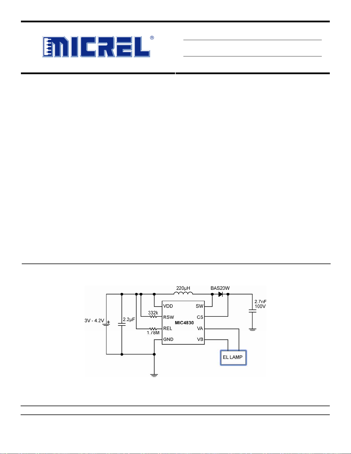
Typical Application
Low Noise EL Driver
MLF and MicroLeadFrame are registered trademark of Amkor Technology, Inc.
Micrel Inc. • 2180 Fortune Drive • San Jose, CA 95131 • USA • tel +1 (
November 2007
408
) 944-0800 • fax + 1 (408) 474-1000 • http://www.micrel.com
M9999-111507-B
Page 2
Micrel MIC4830
Ordering Information
Part Number Junction Temp. Range Package Lead Finish
MIC4830YML –40° to +85°C 8-Pin 3mm × 3mm MLF® RoHS Compliant / Pb-Free / Halogen Free*
MIC4830YMM –40° to +85°C 8-Pin MSOP RoHS Compliant / Pb-Free
Note
*MLF® is a GREEN RoHS compliant package. Lead finish is NiPdAu. Mold compound is Halogen Free.
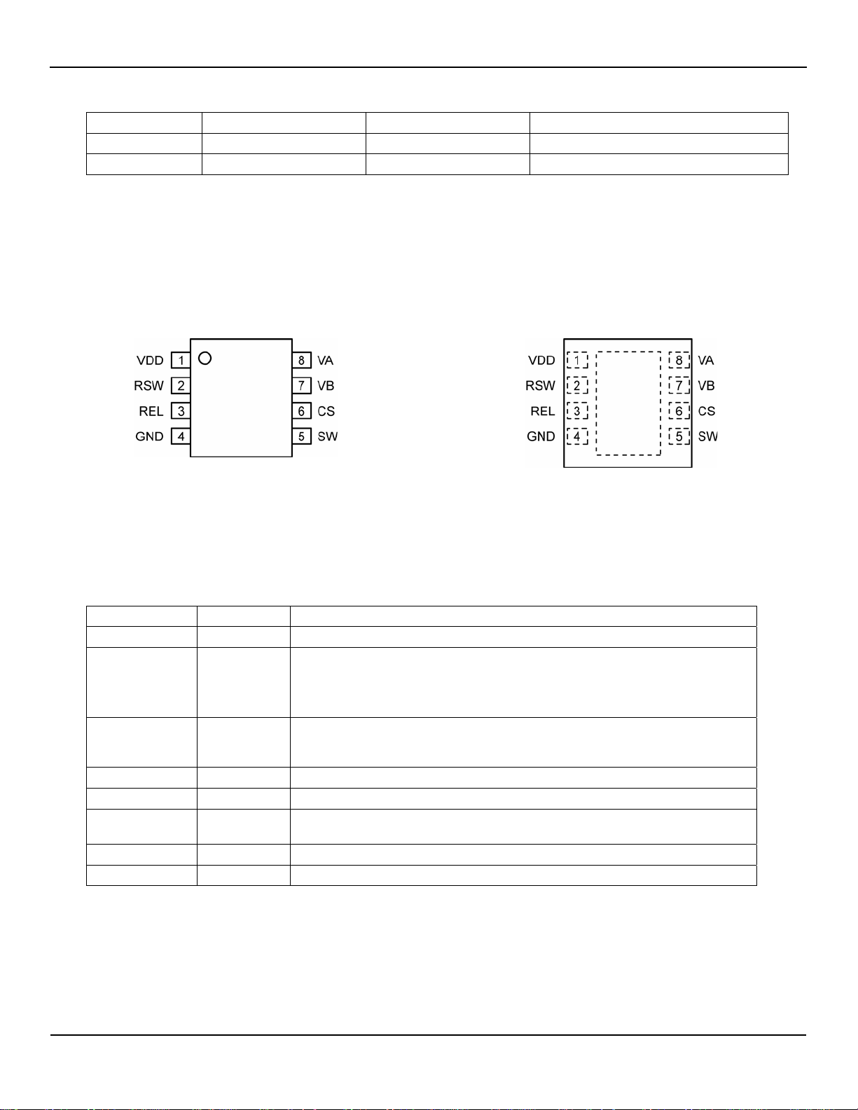
Pin Configuration
Pin Description
Pin Number Pin Name Pin Function
1 VDD Supply (Input): 1.8V to 5.5V for internal circuitry.
2 RSW
3 REL
4 GND Ground
5 SW Switch Node (Input): Internal high-voltage power MOSFET drain.
6 CS
7 VB EL Output: Connect to one end of the EL lamp. Polarity is not important.
8 VA EL Output: Connect to one end of the EL lamp. Polarity is not important.
8-Pin MSOP (MM)
8-Pin 3mm × 3mm MLF
Switch Resistor (External Component): Set switch frequency of the internal
power MOSFET by connecting an external resistor to VDD. Connecting the
external resistor to GND disables the switch oscillator and shuts down the
device.
EL Resistor (External Component): Set EL frequency of the internal H-bridge
driver by connecting an external resistor to VDD. Connecting the external
resistor to GND disables the EL oscillator.
Regulated Boost Output (External Component): Connect to the output capacitor
of the boost regulator and connect to the cathode of the diode.
®
(ML)
November 2007 2
M9999-111507-B
Page 3
Micrel MIC4830
Absolute Maximum Ratings
(1)
Operating Ratings
(2)
Supply Voltage (VDD)...................................... –0.5V to 6.0V
Output Voltage (V
EL Lamp Terminals (V
) ..................................... –0.5V to 120V
CS
, VB)................................... V
A
CS
+ 3V
Switch Voltage (Vsw)…………………………..-0.5V to 120V
Frequency Control Voltage
(V
Storage Temperature (T
ESD Rating
RSW
,
V
) .................................... –0.5V to (VDD+0.3V)
REL
).........................–65°C to +150°C
(4)
............................................................... 1.5kV
S
Supply Voltage (VDD).................................... +1.8V to +5.5V
Lamp Drive Frequency (f
Switching Frequency (f
Ambient Temperature (T
Package Thermal Resistance
) ....................... 60Hz to 1000Hz
EL
).........................65kHz to 250kHz
SW
) ..........................–40°C to +85°C
A
(3)
MSOP (θJA) ......................................................206°C/W
MLF-8L (θ
) ......................................................63°C/W
JA
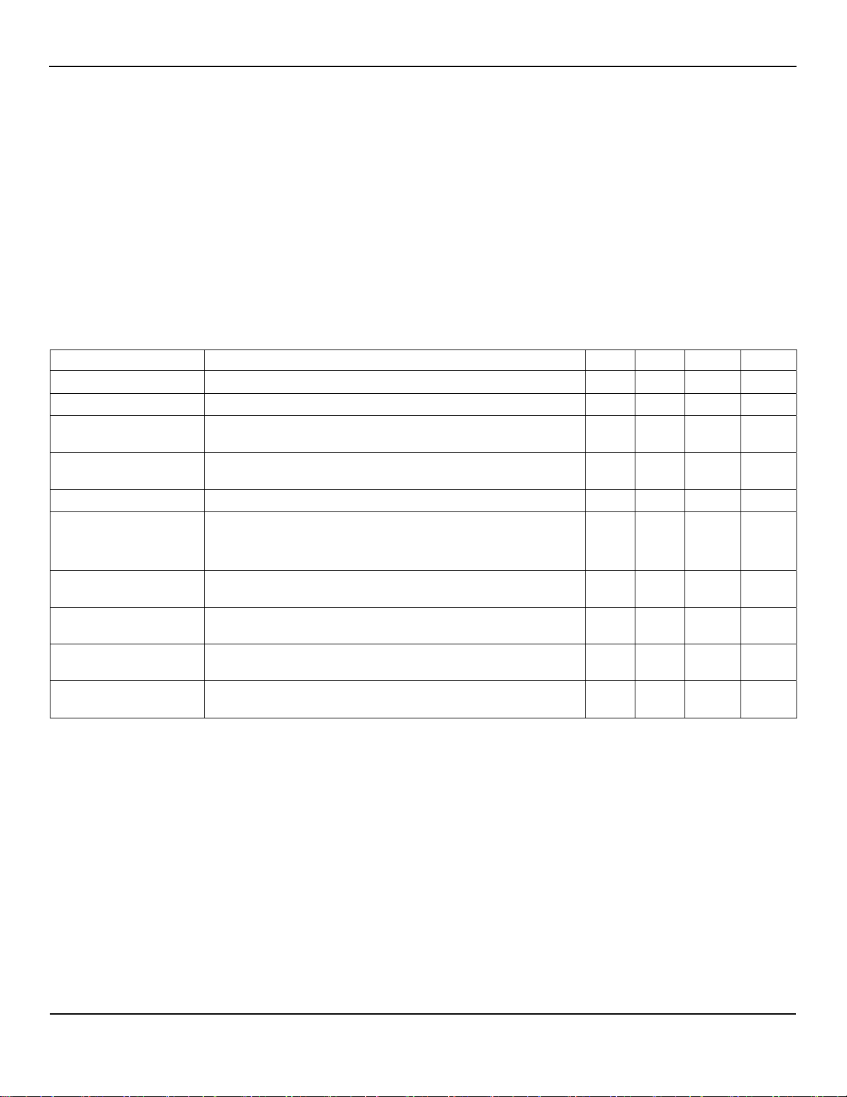
Electrical Characteristics
VIN = VDD = 3.0V, RSW = 332K, REL = 1.78M. TA = 25°C unless otherwise specified. Bold values indicate –40°C TA +85°C.
Parameter Condition Min Typ Max Units
On-resistance ISW = 100mA 3.8 7
CS Voltage Variation VDD = 1.8V to 5.5V
Enable Input Low
Voltage (turn-off)
Enable Input High
Voltage (turn-on)
Shutdown current
Input supply current
Input current including
inductor
VA – VB output drive
frequency
Switching transistor
frequency
Switching transistor duty
cycle
Notes:
1. Exceeding the absolute maximum rating may damage the device.
2. The device is not guaranteed to function outside its operating rating.
3. The maximum allowable power dissipation of any T
power dissipation will result in excessive die temperature.
4. Devices are ESD sensitive. Handling precautions recommended. Human body model, 1.5k in series with 100pF.
5. Specification for packaged product only.
VDD = 1.8V to 5.5V
VDD = 1.8V to 5.5V VDD-
R
SW
R
SW
R
EL
V
CS
V
IN
L=220µH; R
REL=1.78M
RSW = 332K
(5)
Resistor = LOW; REL Resistor = LOW; VDD = 5.5V
Resistor = HIGH;
Resistor = HIGH;
= 90V; VA, VB OPEN
= VDD = 3.2V; RSW = 290K; REL = 1.78M;
= 10k; Lamp = 2in2
OUT
(ambient temperature) is P
A
D(max)
= (T
76
88
99
0.5 V
0.5
0.01
45
0.5
75
15 mA
158 200 242 Hz
90 112 134 kHz
90
– TA) / θθθθJA. Exceeding the maximum allowable
J(max)
V
V
µA
µA
%
November 2007 3
M9999-111507-B
Page 4
Micrel MIC4830
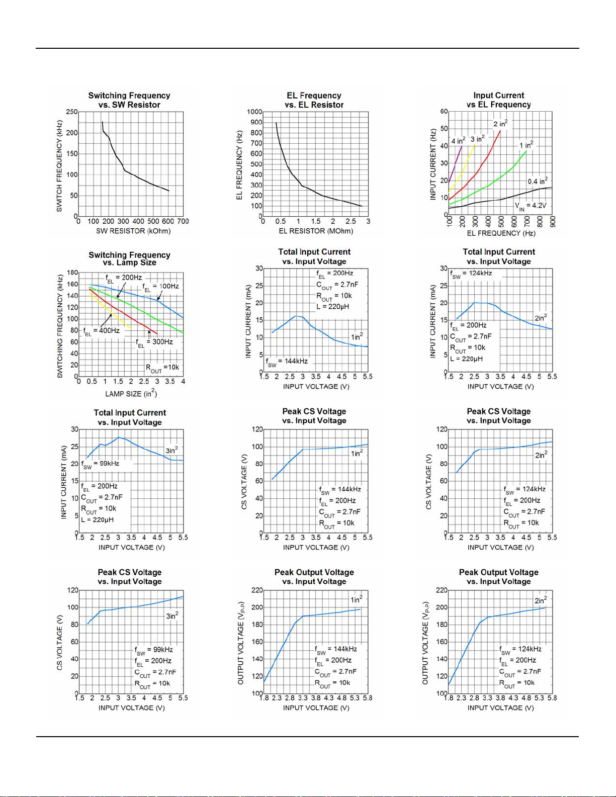
Typical Characteristics
November 2007 4
M9999-111507-B
Page 5

Micrel MIC4830
November 2007 5
M9999-111507-B
Page 6

Micrel MIC4830
Functional Diagram
Figure 1. MIC4830 Block Diagram
Functional Description
Overview
The MIC4830 is a high-voltage EL driver with an AC
output voltage of 180V peak-to-peak capable of
driving EL lamps up to 4 in
2
. Input supply current for
the MIC4830 is typically 45µA reducing to 10nA in
shutdown. The high voltage EL driver has two
internal oscillators to control the switching MOSFET
and the H-bridge driver. Both of the internal
oscillators’ frequencies can be individually
programmed through the external resistors to
maximize the efficiency and the brightness of the EL
lamp.
Regulation
Referring to Figure 1, initially power is applied to
V
. The internal feedback voltage is less than the
DD
reference voltage causing the internal comparator to
go low which enables the switching MOSFET’s
oscillator. When the switching MOSFET turns on,
current flows through the inductor and flows into the
switch. The switching MOSFET will typically turn on
for 90% of the switching period. During the on-time,
energy is stored in the inductor. When the switching
MOSFET turns off, current flowing into the inductor
forces the voltage across the inductor to reverse
polarity. The voltage across the inductor rises until
the external diode conducts and clamps the voltage
at V
discharged into the C
+ VD1. The energy in the inductor is then
OUT
capacitor. The internal
OUT
comparator continues to turn the switching MOSFET
on and off until the internal feedback voltage is
above the reference voltage. Once the internal
feedback voltage is above the reference voltage, the
internal comparator turns off the switching
MOSFET’s oscillator.
When the EL oscillator is enabled, V
and VB switch
A
in opposite states to achieve an 180V peak-to-peak
AC output signal. The external resistor that connects
to the REL pin determines the EL frequency.
November 2007 6
M9999-111507-B
Page 7

Micrel MIC4830
VIN = 3.6V
I
= 12mA
VA
(50V/div)
VB
(50V/div)
VA - V B
(100V/div)
Time (2ms/div)
IN
L = 220µH
C
= 2.7nF
OUT
LAMP = 2 in
RSW = 250k
= 2.82M
R
EL
2
Figure 2. 100Hz Output Waveform
Switching Frequency
The switching frequency of the converter is
controlled via an external resistor between R
and V
pin of the device. The switching frequency
DD
SW
pin
increases as the resistor value decreases. For
resistor value selections, see the “Typical
Characteristics: Switching Frequency vs. SW
Resistor” or use the equation below. The switching
frequency range is 65kHz to 250kHz, with an
accuracy of ±20%. In general, the lower the
switching frequency, the greater the input current is
drawn to deliver more power to the output.
However, the switching frequency should not be so
low as to allow the voltage at the switch node or the
CS pin to go beyond the absolute maximum voltage
of those pins.
36
SW
(kHz)f
SW
()
Ω=MR
EL Frequency
The EL lamp frequency is controlled via an external
resistor connected between R
pin and VDD pin of
EL
the device. The lamp frequency increases as the
resistor value decreases. For resistor value
selections, see the “Typical Characteristics: EL
Frequency vs. EL Resistor” graph on page 4 or use
the equation below. The EL lamp frequency range is
60Hz to 1000Hz, with an accuracy of ±20%.
VIN = 3.6V
I
= 19mA
VA
(50V/div)
VB
(50V/div)
VA - V B
(100V/div)
Time (2ms/div)
IN
L = 220µH
C
= 2.7nF
OUT
LAMP = 2 in
RSW = 290k
= 1.69M
R
EL
2
Figure 3. 200Hz Output Waveform
In general, as the EL lamp frequency increases, the
amount of current drawn from the battery will
increase. The color of the EL lamp and the intensity
are dependent upon its frequency.
VIN = 3.6V
I
= 25mA
VA
(50V/div)
VB
(50V/div)
VA - V B
(100V/div)
Time (2ms/div)
IN
L = 220µH
C
= 2.7nF
OUT
LAMP = 2 in
RSW = 352k
= 1.1M
R
EL
2
Figure 4. 300Hz Output Waveform
Enable Function
The MIC4830 is disabled by connecting the external
resistor (Rsw) to GND. This turns off the switch
oscillator of the boost converter. Connecting the
external resistor (Rsw) to V
enables the oscillator
DD
and turns on the device. The enable voltage should
rise or fall monotonically without interruption.
()
Hzf
EL
360
EL
()
Ω=MR
November 2007 7
M9999-111507-B
Page 8

Micrel MIC4830
Application Information
Inductor
A 220µH Murata (LQH4C221K04) inductor is
recommended for most applications. Generally,
inductors with smaller values can handle more
current. Lowering the inductance allows the boost
regulator to draw more input current to deliver more
energy every cycle. As a result, a lower value
inductor may be used to drive larger panels or make
the current panel brighter. However, caution is
required as using a low value inductor with a low
switching frequency may result in voltages
exceeding the absolute maximum rating of the
switch node and/or the CS pin. If the application
uses a low input voltage (1.8 to 3V), a lower value
inductor, such as 100µH, may be used in order to
drive the EL lamp at max brightness without issue.
Diode
An ideal diode to use would be the 1N4148 or
equivalent. It has a forward current of 150mA and a
typical forward voltage of 950mV. For applications
that are not cost driven, a fast switching diode with
lower forward voltage and higher reverse voltage
can be used to enhance the efficiency, such as
BAV20WS or BAS20W.
Output Capacitor
Low ESR capacitors should be used at the regulated
boost output (CS pin) of the MIC4830 to minimize
the switching output ripple voltage. The larger the
output capacitance, the lower the output ripple at the
CS pin. The reduced output ripple at the CS pin
along with a low ESR capacitor improves the
efficiency of the MIC4830 circuit. Selection of the
capacitor value will depend upon the peak inductor
current, inductor size, and the load. The MIC4830 is
designed for use with an output capacitance as low
as 2.2nF. For minimum audible noise, the use of a
C0G/NPO dielectric output capacitor is
recommended. TDK and AVX offer C0G/NPO
dielectric capacitors in capacitances up to 2.7nF at
200V to 250V rating in 0805 size. If output ripple is a
concern a 0.01µF/200V X7R output capacitor is
recommended.
EL Lamp Terminals (VA, VB)
An EL lamp is connected from VA to VB as the load.
The high voltage alternated across VA and VB by
the H-Bridge cycles generate luminance. The
voltage at VA and VB should not exceed the voltage
at V
by more than 3V. This situation may become
CS
present when noisy enable signals such as those
often generated by mechanical switches are applied
to the driver’s inputs. To prevent over voltage at VA
and VB, 10kΩ resistors may be placed in series from
VA to the EL panel and from VB to the EL panel. An
alternative to the use of 10kΩ resistors is to apply a
diode from the CS pin to VA and VB, where the
cathode of the diode is on the CS side and the
anode is on the VA and VB side, respectively.
November 2007 8
M9999-111507-B
Page 9

Micrel MIC4830
Application Circuit
Figure 5: Typical Li-Ion Powered MIC4830 Circuit
Size
(inch
2
)
Capacitance
(nF)
Lamp Frequency
0.4 2
1 5
2 10
3 15
4 20
Note: Table 1 applies to circuit shown in Figure 5.
Table 1: Recommended RSW & REL values for various panel sizes
(Hz)
R
EL
(MΩ)
RSW (kΩ)
SW
(kHz)
f
RSW (kΩ)
SW
(kHz)
f
RSW (kΩ)
SW
(kHz)
f
RSW (kΩ)
SW
(kHz)
f
RSW (kΩ)
SW
(kHz)
f
100 200 300 400 500 600 700 800 900
2.82 1.69 1.1 0.837 0.665 0.562 0.471 0.409 0.369
225 232 237 248 257 269 281 300 321
160 155 152 145 140 134 128 120 112
232 250 277 300 346 395 473
155 144 130 120 104 91 76
250 290 352 433 521
144 124 102 83 69
272 363 480
132 99 75
353 473
102 76
November 2007 9
M9999-111507-B
Page 10

Micrel MIC4830
Layout Recommendation
Top
Bottom
November 2007 10
M9999-111507-B
Page 11

Micrel MIC4830
Package Information
8-Pin MSOP (MM)
8-Pin 3mm x 3mm MLF (ML)
November 2007 11
M9999-111507-B
Page 12

Micrel MIC4830
MICREL, INC. 2180 FORTUNE DRIVE SAN JOSE, CA 95131 USA
TEL +1 (408) 944-0800 FAX +1 (408) 474-1000 WEB http:/www.micrel.com
The information furnished by Micrel in this data sheet is believed to be accurate and reliable. However, no responsibility is assumed by Micrel for its
Micrel Products are not designed or authorized for use as components in life support appliances, devices or systems where malfunction of a product
can reasonably be expected to result in personal injury. Life support devices or systems are devices or systems that (a) are intended for surgical implant
into the body or (b) support or sustain life, and whose failure to perform can be reasonably expected to result in a significant injury to the user. A
Purchaser’s use or sale of Micrel Products for use in life support appliances, devices or systems is a Purchaser’s own risk and Purchaser agrees to fully
use. Micrel reserves the right to change circuitry and specifications at any time without notification to the customer.
indemnify Micrel for any damages resulting from such use or sale.
© 2007 Micrel, Incorporated.
November 2007 12
M9999-111507-B
 Loading...