

Page 1

MIC4807 Micrel
MIC4807
80V 8-Channel Addressable Low-Side Driver
General Description
The MIC4807 is an 80V, 8-channel, addressable low side
driver with latches and TTL/CMOS compatible logic inputs.
Each logic input is composed of a comparator with a 1.4V
bandgap-derived reference serving as the trip point. The
addresses (AIN, BIN, and CIN) and Data-in logic inputs have an
internal 50µA pull-up current source, while the Output Enable
(OE), Chip Select (CS), and Clear logic inputs have an
internal 75µA pull-down sink. If the logic lines to the MIC4807
are severed, these currents guarantee that the outputs will
turn OFF.
Individual latches in the MIC4807 are selected by a binary
address presented at inputs AIN, BIN, and CIN. Data-in is
directed to the addressed latch while CS is held low, allowing
an individual output to be pulse-width modulated. When CS
is set high again, the last Data-in is stored in the latch. If Datain = "1", the addressed output is turned on, and if Data-in = "0",
the addressed output is turned off.
Information presented to Data-in and the address inputs is
transferred to the latches while CS is pulled low. For
application, where several outputs must be (Continued)
Pin Diagram
Features
• 4.5V to 16V Operation
• Eight 80V 100mA Outputs
• Off-state Leakage less than 10µA at 25°C
• Short-Circuit Proof
• Thermal Shutdown with Hysteresis
• DMOS Output Devices (RON ≤ 7Ω at 25°C)
Applications
• Lamp Drivers
• Solenoid Drivers
• Display Drivers
-Electroluminescent
-Vacuum Fluorescent
-Plasma
• Relay Drivers
• Print Head Drivers
• Heater Drivers
• Power Semiconductor Drivers
• Security Systems
• Environmental Controls
• Process Controllers
Ordering Information
VDD
OE
CS
Clear
1
2
3
4
MIC4807
5
6
7
8
HVOUT2
HVOUT3
Ground
HVOUT4
HVOUT5
Block Diagram
18
17
16
15
14
13
12
11
109
Addressing
HVOUT1
HVOUT0
Data-in
AIN
BIN
CIN
VDD
HVOUT7
HVOUT6
V
DD
A
IN
B
IN
{
C
IN
Data-in
Ground
12
15
14
13
16
Part Operating Package
7
Number Temperature-Range
MIC4807BN -40°C to 85°C 18-Pin Plastic DIP
Thermal
Shutdown
Address
Decoder
5
647
CS
Latches
Current
Limit
Driver
•
•
•
•
•
•
Driver
OEClear
17
18
10
11
1
2
8
9
HVOUT
HVOUT
HVOUT
HVOUT
HVOUT
HVOUT
HVOUT
HVOUT
0
1
2
3
4
5
6
7
October 1998 7-3
Page 2
MIC4807 Micrel
General Description (Continued)
turned on simultaneously, Gray Code address sequencing
can be applied to Ain, Bin, Cin, while Data-in is held high and
CS is held low. Data-in will be transferred to each address in
turn, without the need to toggle CS. Similarly, a set of outputs
could be simultaneously turned off by setting Data-in low.
Gray Code ensures that no intermediate addresses are
inadvertently accessed. A typical Gray Code is 0, 1, 3, 2, 6,
7, 5, 4.
Each output drive circuit has a high-voltage, power DMOS
device configured as a transconductance loop. This loop
limits the output current to typically 200mA. While current
limiting keeps the output device within its allowable safeoperating area (SOA), the power dissipation may be excessive. Long-term survival is guaranteed by thermal shutdown.
When operated below current limit, the outputs appear as
small-valued resistors (typically 5.1Ω at 25°C) connected to
ground. The "ON" resistance (RON) has a strong, positive
temperature coefficient (approximately 7500 ppm/°C) which
promotes current sharing if two or more outputs are paral-
leled.
Absolute Maximum Ratings (Notes 1, 2 and 3)
Output Voltage (V
Supply Voltage (VDD) 16.5V
Logic Input Voltage (VIN) –0.3V TO VDD + 0.3
Continuous Output Current (I
Power Dissipation (PD, Note 2) Internally Limited
Ambient Temperature (TA): –40°C to +85°C
Maximum Junction Temperature (T
Storage Temperature –65°C to +150°C
, OFF) 100V
OUT
) Internally Limited
OUT
) 150°C
JMAX
θJA - Plastic DIP 130°C/W
Electrical Characteristics: (Note 6) MIC4807BN, T
= 25°C, VDD = 15V unless otherwise specified (see
A
Test Circuit).
Symbol Parameter Conditions Min Typ Max Units
V
DD
I
DD
(0) Logic Input Voltage 4.5V ≤ VDD ≤ 16V 0.8 V
V
IN
VIN (1) 2.0 V
I
(0) Logic Input Current for AIN,V
IN
I
(1) Logic Input Current for CS, VIN = V
IN
I
OUT
R
ON
I
SC
V
OUT
V
OUT
Supply Voltage 4.5 16 V
Supply Current OE = L (Note 3) 5.5 10 mA
OE = H (Note 4) 1.5 3 mA
= 0V –150 –70 –25 µA
B
, CIN, and Data-in
IN
OE, and Clear
Output Leakage Current OE = 0V, V
Output "ON" Resistance Output is ON, V
Short Circuit Current Output is ON< V
Output Voltage (OFF) 80 V
Output Voltage (ON) I
IN
DD
= 80V 1 10 µA
OUT
= 0.7V,V
OUT
= 50V 140 190 250 mA
OUT
10V ≤ V
OUT
I
OUT
≤ 15V (Note 5)
DD
= 50mA,VDD = 10V 0.26 0.35 V
= 100mA, VDD = 10V 0.51 0.7 V
= 10V 5.1 7 Ω
DD
25 130 250 µA
Data and Address V
Set-up Time (A, see Timing Diagram)
Data and Address (B) 50 ns
Hold Time
CS Pulse Width (C) 500 ns
Turn-on Delay (D) 2.5 ns
= 10V for all timing tests 400 ns
DD
7-4 October 1998
Page 3

MIC4807 Micrel
Electrical Characteristics: (Note 6) T
Symbol Parameter Conditions Min Typ Max Units
Turn-Off Delay (E) 2.5 µs
Output Disable (F) 2 µs
Response Time
Output Enable (G) 2 µs
Response Time
Clear Response Time (H) 2.5 µs
Clear Pulse Width (I) 500 ns
Electrical Characteristics: (Note 6) T
= 25°C, VDD = 15V unless otherwise specified (see Test Circuit).
A
= –55°C to +125°C, VDD = 15V unless otherwise specified (see Test
A
Circuit).
Symbol Parameter Conditions Min Typ Max Units
V
I
DD
DD
Supply Voltage 4.5 16 V
Supply Current OE = L (Note 3) 15 mA
OE = H (Note 4) 4 mA
(0) Logic Input Voltage 4.5V ≤ VDD ≤ 16V 0.8 V
V
IN
V
(1) 2.0 V
IN
IIN (0) Logic Input Current for AIN,V
, CIN, and Data-in
B
IN
IIN (1) Logic Input Current for CS, VIN = V
OE, and Clear
I
OUT
R
ON
I
SC
V
OUT
V
OUT
Output Leakage Current OE = 0V, V
Output "ON" Resistance Output is ON, V
Short Circuit Current Output is ON< V
Output Voltage (OFF) 80 V
Output Voltage (ON) I
Data and Address VDD = 10V for all timing tests 700 ns
Set-up Time (A, see Timing Diagram)
Data and Address (B) 50 ns
Hold Time
= 0V –250 –10 µA
IN
DD
= 80V 5.1 7 µA
OUT
=0.7V,VDD=10V 12 Ω
OUT
= 50V 100 300 mA
10V ≤ V
I
DD
= 50mA,VDD = 10V 0.6 V
OUT
= 100mA, VDD = 10V 1.2 V
OUT
OUT
≤ 15V (Note 5)
25 400 µA
7
CS Pulse Width (C) 1000 ns
Turn-on Delay (D) 5 µs
October 1998 7-5
Page 4

MIC4807 Micrel
Electrical Characteristics: (Note 6) T
Symbol Parameter Conditions Min Typ Max Units
Turn-Off Delay (E) 5 µs
Output Disable (F) 4 µs
Response Time
Output Enable (G) 4 µs
Response Time
Clear Response Time (H) 5 µs
Clear Pulse Width (I) 1000 ns
Note 1: Absolute Maximum Ratings indicate limits beyond which damage to the device may occur. Electrical specifications do not
apply when operating the device beyond its specified operating ratings.
Note 2: The junction temperature is internally limited by a thermal shutdown circuit. The maximum power dissipation is a function of
T
, θJA, and TA. The maximum allowable power dissipation at any ambient temperature is PD = (T
JMAX
is exceeded, the die temperature will rise above 150°C, and the MIC4807 will go into thermal shutdown.
Note 3: All outputs are off when OUTPUT ENABLE is pulled low.
Note 4: All outputs are turned on during this test.
Note 5: Pulse testing is used to avoid thermal shutown.
Note 6: Minimum and Maximum limits are tested and 100% guaranteed over the temperature range specified. Typicals are measured
at 25°C and represent the most likely parametric norm.
= 25°C, VDD = 15V unless otherwise specified (see Test Circuit).
A
- TA) / θJA. If this dissipation
JMAX
Timing Diagram
CIN
BIN
AIN
Data-in
CS
Clear
OE
HVOUT0
HVOUT1
HVOUT
AB
D
2
Logic "1"
Logic "0"
C
H
G
F
OFF
ON
H
ED
HVOUT3
HVOUT4
7-6 October 1998
Page 5
MIC4807 Micrel
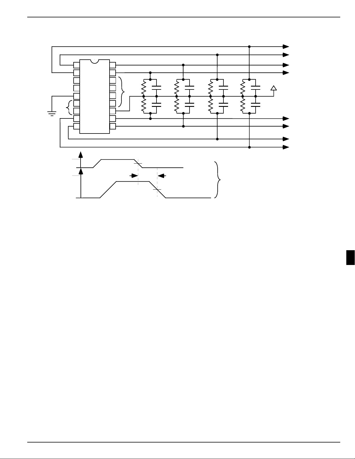
Test Circuit and AC Waveform Measurement Standards
V
OUT3
V
OUT2
V
1
2
3
VDD
VIN
4
MIC4807
5
VIN
IN
V
6
7
8
9
5V
0V
10V
OUT
V
18
17
16
15
14
13
12
11
10
VIN
RCRCRC
tDelay
RCRCRCRC
VDD=10V
RC
All reference times are taken
from the 50% transition point.
OUT1
V
OUT0
C = 35pF
R = 10kΩ
V
OUT7
V
OUT6
V
OUT5
V
OUT4
0V
7
October 1998 7-7
Page 6

MIC4807 Micrel
Equivalent Logic Diagram
DD
V
A
IN
B
IN
C
IN
Data-in
CS
Clear
OE
50µA
+
-
+
-
75µA
1.4V
Address
Decoder
Drive
Circuit
Total of
8 Channels
Drive
Circuit
OVER
TEMP
HVOUT
HVOUT
0
7
CINBINA
IN
CS Data-in Clear OE
T ruth Tab le
CS Clear Data-In CINBINAINOE HVOUT0HVOUT1HVOUT2HVOUT3HVOUT4HVOUT5HVOUT6HVOUT
X L X X X X X H H H H H H H H Clear
H H X X X X H P P P P P P P P Memory
L H D L L L H D P P P P P P P Address HVOUT
L H D L L H H P D P P P P P P Address HVOUT
L H D L H L H P P D P P P P P Address HVOUT
L H D L H H H P P P D P P P P Address HVOUT
L H D H L L H P P P P D P P P Address HVOUT
L H D H L H H P P P P P D P P Address HVOUT
L H D H H L H P P P P P P D P Address HVOUT
L H D H H H H P P P P P P P D Address HVOUT
X X X X X X L H H H H H H H H Blanking
L = Low Logic Level X = Don't Care
H = High Logic Level P = Previous State
D = Data (High or Low)
Functional Mode
7
0
1
2
3
4
5
6
7
7-8 October 1998
Page 7

MIC4807 Micrel
Typical DC Output Characteristics for the “On” State:
(VDD = 10V and TA = 25°C unless other wise specified)
VDD = 10V
VDD = 15V
SHORT CIRCUIT CURRENT
400
EXPANDED VERSION OF SHORT
CIRCUIT CURRENT FOR LOW
OUTPUT VOLTAGE (V
400
OUT)
300
200
(mA)
OUT
I
100
120
100
80
60
(mA)
OUT
I
40
300
200
(mA)
OUT
I
100
0
806040200
(V)
V
OUT
FOR SEPARATE V
I
OUT
DD
0
012345
V
(V)
OUT
I
AT 3 TEMPERATURES
OUT
120
T = –55°C T = 25°C
100
80
(mA)
60
OUT
I
40
T = 125°C
7
20
0
0
0.5 1.0
V
(V)
OUT
SHORT CIRCUIT CURRENT LIMIT (I
200
100
(mA)
SC
I
0
0.0 5.0
(V)
V
DD
SC
10.0
20
0
0.0 5.0 10.0
V
(V)
OUT
)
ON RESISTANCE (R
ON
)
15.0
10.0
(Ω)
ON
R
5.0
0.0
0.0 5.0
V
DD
(V)
10.0
October 1998 7-9
Page 8

MIC4807 Micrel
Pin Description
Pin No. Pin Name Functional Description
5 Ground Electrical ground to chip substrate.
12 V
DD
1, 2, 8, HVOUT0 through HVOUT
7
Positive logic supply voltage (10V-15V).
These are the high voltage (HV) open outputs, each of which is capable of
9,10, 11, sinking 100mA when switched on, and standing off 80V when switched off.
17,18 In addition, each output channel is equipped with an analog current limiter
to protect it from shorts to the positive high voltage supply. When an output
is shorted (up to 80V), a maximum of 225mA (200mA nominal) will flow
through it to ground.
13, 14, 15 CIN, BIN, &A
IN
When these inputs are combined together they form the BCD address used
to select the desired output. Each input is TTL compatible with an internal
pull-up current source of 50mA.
6 CS When CS is at logic "0" the device is actively addressed, and when CS is
at logic "1" the decoded address and input Data are inhibited, making
the part unaddressable. CS is TTL compatible with an internal pull-down
current sink of 75µA.
7 Clear Clear resets all the outputs to the off state when pulled to logic "0", and is
TTL compatible with an internal pull-down current sink of 75µA.
16 Data-in Data-in determines the state of the output being addressed. When Data-
in is at logic "0" the addressed output is turned off, and when Data-in is at
logic "1" the addressed output is turned on. Data-in is TTL compatible with
an internal pull-up current source of 50µA.
4 OE OE allows the bank of eight outputs to be duty cycled together. When OE
is at logic "1" the outputs are enabled to follow their respective latches, and
when OE is at logic "0" all the outputs are turned off. OE is TTL Compatible
with a pull-down current sink of 75µA.
7-10 October 1998
 Loading...