

Page 1
September 1999 1 MIC4426/4427/4428
MIC4426/4427/4428 Micrel
MIC4426/4427/4428
Dual 1.5A-Peak Low-Side MOSFET Driver
General Description
The MIC4426/4427/4428 family are highly-reliable dual lowside MOSFET drivers fabricated on a BiCMOS/DMOS process for low power consumption and high efficiency. These
drivers translate TTL or CMOS input logic levels to output
voltage levels that swing within 25mV of the positive supply
or ground. Comparable bipolar devices are capable of swinging only to within 1V of the supply. The MIC4426/7/8 is
available in three configurations: dual inverting, dual noninverting, and one inverting plus one noninverting output.
The MIC4426/4427/4428 are pin-compatible replacements
for the MIC426/427/428 and MIC1426/1427/1428 with improved electrical performance and rugged design (Refer to
the Device Replacement lists on the following page). They
can withstand up to 500mA of reverse current (either polarity)
without latching and up to 5V noise spikes (either polarity) on
ground pins.
Primarily intended for driving power MOSFETs, MIC4426/7/8
drivers are suitable for driving other loads (capacitive, resistive, or inductive) which require low-impedance, high peak
current, and fast switching time. Other applications include
driving heavily loaded clock lines, coaxial cables, or piezoelectric transducers. The only load limitation is that total driver
power dissipation must not exceed the limits of the package.
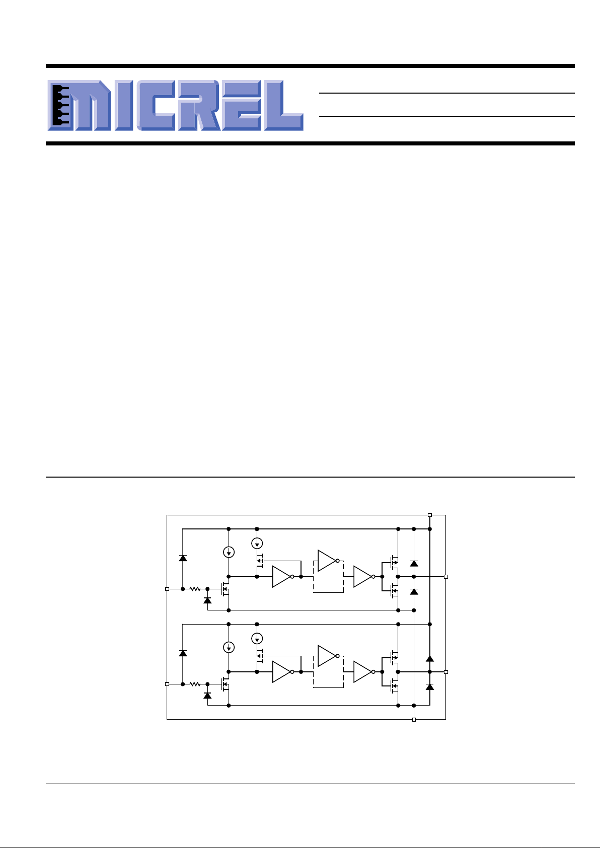
Functional Diagram
INA
OUTA
INVERTING
NONINVERTING
0.1mA
0.6mA
2kΩ
INB
OUTB
INVERTING
NONINVERTING
0.1mA
0.6mA
2kΩ
V
S
GND
Features
• Bipolar/CMOS/DMOS construction
• Latch-up protection to >500mA reverse current
• 1.5A-peak output current
• 4.5V to 18V operating range
• Low quiescent supply current
4mA at logic 1 input
400µA at logic 0 input
• Switches 1000pF in 25ns
• Matched rise and rall times
•7Ω output impedance
• < 40ns typical delay
• Logic-input threshold independent of supply voltage
• Logic-input protection to –5V
• 6pF typical equivalent input capacitance
• 25mV max. output offset from supply or ground
• Replaces MIC426/427/428 and MIC1426/1427/1428
• Dual inverting, dual noninverting, and inverting/
noninverting configurations
• ESD protection
Applications
• MOSFET driver
• Clock line driver
• Coax cable driver
• Piezoelectic transducer driver
Page 2

MIC4426/4427/4428 Micrel
MIC4426/4427/4428 2 September 1999
Pin Description
Pin Number Pin Name Pin Function
1, 8 NC not internally connected
2 INA Control Input A: TTL/CMOS compatible logic input.
3 GND Ground
4 INB Control Input B: TTL/CMOS compatible logic input.
5 OUTB Output B: CMOS totem-pole output.
6V
S
Supply Input: +4.5V to +18V
7 OUTA Output A: CMOS totem-pole output.
Pin Configuration
1
2
3
4
8
7
6
5
NC
INA
GND
INB
NC
OUTA
V
S
OUTB
MIC4426
Dual
Inverting
A
B
7
5
2
4
MIC4426 MIC4427 MIC4428
A
B
7
5
2
4
A
B
7
5
2
4
1
2
3
4
8
7
6
5
NC
INA
GND
INB
NC
OUTA
V
S
OUTB
MIC4427
Dual
Noninverting
1
2
3
4
8
7
6
5
NC
INA
GND
INB
NC
OUTA
V
S
OUTB
MIC4428
Inverting +
Noninverting
Ordering Information
Part Number Temperature Range Package Configuration
MIC4426AM –55°C to +125°C 8-lead SOIC Dual Inverting
MIC4426BM –40°C to +85°C 8-lead SOIC Dual Inverting
MIC4426BMM –40°C to +85°C 8-lead MSOP Dual Inverting
MIC4426BN –40°C to +85°C 8-lead Plastic DIP Dual Inverting
MIC4427AM –55°C to +125°C 8-lead SOIC Dual Noninverting
MIC4427BM –40°C to +85°C 8-lead SOIC Dual Noninverting
MIC4427BMM –40°C to +85°C 8-lead MSOP Dual Noninverting
MIC4427BN –40°C to +85°C 8-pin Plastic DIP Dual Noninverting
MIC4428AM –55°C to +125°C 8-lead SOIC Inverting + Noninverting
MIC4428BM –40°C to +85°C 8-lead SOIC Inverting + Noninverting
MIC4428BMM –40°C to +85°C 8-lead MSOP Inverting + Noninverting
MIC4428BN –40°C to +85°C 8-lead Plastic DIP Inverting + Noninverting
MIC426/427/428 Device Replacement
Discontinued Number Replacement
MIC426CM MIC4426BM
MIC426BM MIC4426BM
MIC426CN MIC4426BN
MIC426BN MIC4426BN
MIC427CM MIC4427BM
MIC427BM MIC4427BM
MIC427CN MIC4427BN
MIC427BN MIC4427BN
MIC428CM MIC4428BM
MIC428BM MIC4428BM
MIC428CN MIC4428BN
MIC428BN MIC4428BN
MIC1426/1427/1428 Device Replacement
Discontinued Number Replacement
MIC1426CM MIC4426BM
MIC1426BM MIC4426BM
MIC1426CN MIC4426BN
MIC1426BN MIC4426BN
MIC1427CM MIC4427BM
MIC1427BM MIC4427BM
MIC1427CN MIC4427BN
MIC1427BN MIC4427BN
MIC1428CM MIC4428BM
MIC1428BM MIC4428BM
MIC1428CN MIC4428BN
MIC1428BN MIC4428BN
Page 3
September 1999 3 MIC4426/4427/4428
MIC4426/4427/4428 Micrel
Absolute Maximum Ratings (Note 1)
Supply Voltage (VS) ....................................................+22V
Input Voltage (VIN) .........................VS + 0.3V to GND – 5V
Junction Temperature (TJ) ........................................ 150°C
Storage Temperature ............................... –65°C to +150°C
Lead Temperature (10 sec.)...................................... 300°C
ESD Rating, Note 3
Operating Ratings (Note 2)
Supply Voltage (VS) ..................................... +4.5V to +18V
Temperature Range (TA)
(A) ........................................................ –55°C to +125°C
(B) .......................................................... –40°C to +85°C
Package Thermal Resistance
PDIP θJA............................................................130°C/W
PDIP θJC.............................................................42°C/W
SOIC θJA...........................................................120°C/W
SOIC θJC.............................................................75°C/W
MSOP θJC.........................................................250°C/W
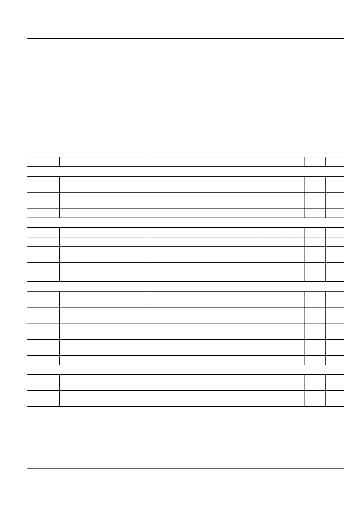
Electrical Characteristics
4.5V ≤ Vs ≤ 18V; TA = 25°C, bold values indicate full specified temperature range; unless noted.
Symbol Parameter Condition Min Typ Max Units
Input
V
IH
Logic 1 Input Voltage 2.4 1.4 V
2.4 1.5 V
V
IL
Logic 0 Input Voltage 1.1 0.8 V
1.0 0.8 V
I
IN
Input Current 0 ≤ VIN ≤ V
S
–1 1 µA
Output
V
OH
High Output Voltage
VS–0.025
V
V
OL
Low Output Voltage 0.025 V
R
O
Output Resistance I
OUT
= 10mA, VS = 18V 6 10 Ω
812Ω
I
PK
Peak Output Current 1.5 A
I Latch-Up Protection withstand reverse current >500 mA
Switching Time
t
R
Rise Time test Figure 1 18 30 ns
20 40 ns
t
F
Fall Time test Figure 1 15 20 ns
29 40 ns
t
D1
Delay Tlme test Flgure 1 17 30 ns
19 40 ns
t
D2
Delay Time test Figure 1 23 50 ns
27 60 ns
t
PW
Pulse Width test Figure 1 400 ns
Power Supply
I
S
Power Supply Current V
INA
= V
INB
= 3.0V 1.4 4.5 mA
1.5 8 mA
I
S
Power Supply Current V
INA
= V
INB
= 0.0V 0.18 0.4 mA
0.19 0.6 mA
Note 1. Exceeding the absolute maximum rating may damage the device.
Note 2. The device is not guaranteed to function outside its operating rating.
Note 3. Devices are ESD sensitive. Handling precautions recommended.
Page 4

MIC4426/4427/4428 Micrel
MIC4426/4427/4428 4 September 1999
Test Circuits
A
B
INA
INB
2
4
MIC4427
5
7
OUTA
1000pF
6
VS = 18V
0.1µF 4.7µF
OUTB
1000pF
Figure 2a. Noninverting Configuration
90%
10%
t
R
10%
0V
5V
t
F
V
S
OUTPUT
INPUT
90%
0V
t
D1
t
D2
t
PW
2.5V
Figure 2b. Noninverting Timing
A
B
INA
INB
2
4
MIC4426
5
7
OUTA
1000pF
6
VS = 18V
0.1µF 4.7µF
OUTB
1000pF
Figure 1a. Inverting Configuration
t
D1
90%
10%
t
F
10%
0V
5V
t
D2
t
R
V
S
OUTPUT
INPUT
90%
0V
2.5V
t
PW
Figure 1b. Inverting Timing
Page 5

September 1999 5 MIC4426/4427/4428
MIC4426/4427/4428 Micrel
Electrical Characteristics
Rise and Fall Time vs.
Supply Voltage
05 2010 15
t
F
SUPPLY VOLTAGE (V)
70
60
50
40
10
0
TIME (ns)
20
30
Delay Time vs. Supply Voltage
05 2010 15
SUPPLY VOLTAGE (V)
35
30
25
20
5
0
TIME (ns)
10
15
40
30
10
TIME (ns)
20
-25 0 150
25 50
TEMPERATURE (°C)
75
100
125
Delay Time vs. Temperature
35
30
25
20
5
0
TIME (ns)
10
15
-25 0 15025 50
TEMPERATURE (°C)
75 100125
t
D1
Supply Current vs.
Capacitive Load
80
70
60
50
20
0
SUPPLY CURRENT (mA)
30
40
10
400kHz
200
kHz
20kHz
10 10000100
CAPACITIVE LOAD (pF)
1000
1k
100
10
1
TIME (ns)
10 10000100
CAPACITIVE LOAD (pF)
1000
Rise and Fall Time vs.
Capacitive Load
t
R
t
F
Supply Current vs. Frequency
V = 18V
S
10 V
5 V
20
0
SUPPLY CURRENT (mA)
30
10
1 100010
FREQUENCY (kHz)
100
High Output vs. Current
| V – V | (V)
S OUT
CURRENT SOURCED (mA)
Low Output vs. Current
1.20
0.96
0
0.48
0.72
0.24
010
CURRENT SUNK (mA)
20 30 40 50 60 70 80 90 100
10 V
15 V
OUTPUT VOLTAGE (V)
Rise and Fall Time
vs. Temperature
1.20
0.96
0
0.48
0.72
0.24
0 102030405060708090100
10 V
15 V
-50
t
R
-50
-75
t
R
t
F
-75
t
D2
t
D1
t
D2
C = 1000pF
T = 25°C
L
A
C = 1000pF
T = 25°C
L
A
C = 1000pF
V = 18V
L
S
C = 1000pF
V = 18V
L
S
T = 25°C
V = 18V
A
S
T = 25°C
V = 18V
A
S
T = 25°C
C = 1000pF
L
A
T = 25°C
A
V = 5V
C
T = 25°C
A
V = 5V
S
Quiescent Power Supply
Current vs. Supply Voltage
Package Power Dissipation
25 50 15075 100
AMBIENT TEMPERATURE (°C)
1000
750
250
0
500
Quiescent Power Supply
Current vs. Supply Voltage
0
0.5
2.5
1.0
1.5
SUPPLY CURRENT (mA)
201550
SUPPLY VOLTAGE (V)
10
2.0
125
SUPPLY CURRENT (µA)
151005
0
50
100
150
200
300
400
20
SUPPLY VOLTAGE (V)
MAXIMUM PACKAGE
POWER DISSIPATION (mW)
1250
NO LOAD
BOTH INPUTS LOGIC "1"
T = 25°C
A
NO LOAD
BOTH INPUTS LOGIC "0"
T = 25°C
A
SOIC
PDIP
Page 6

MIC4426/4427/4428 Micrel
MIC4426/4427/4428 6 September 1999
Applications Information
Supply Bypassing
Large currents are required to charge and discharge large
capacitive loads quickly. For example, changing a 1000pF
load by 16V in 25ns requires 0.8A from the supply input.
To guarantee low supply impedance over a wide frequency
range, parallel capacitors are recommended for power supply bypassing. Low-inductance ceramic MLC capacitors with
short lead lengths (< 0.5") should be used. A 1.0µF film
capacitor in parallel with one or two 0.1µF ceramic MLC
capacitors normally provides adequate bypassing.
Grounding
When using the inverting drivers in the MIC4426 or MIC4428,
individual ground returns for the input and output circuits or a
ground plane are recommended for optimum switching speed.
The voltage drop that occurs between the driver’s ground and
the input signal ground, during normal high-current switching,
will behave as negative feedback and degrade switching
speed.
Control Input
Unused driver inputs must be connected to logic high (which
can be VS) or ground. For the lowest quiescent current
(< 500µA) , connect unused inputs to ground. A logic-high
signal will cause the driver to draw up to 9mA.
The drivers are designed with 100mV of control input hysteresis. This provides clean transitions and minimizes output
stage current spikes when changing states. The control input
voltage threshold is approximately 1.5V. The control input
recognizes 1.5V up to VS as a logic high and draws less than
1µA within this range.
The MIC4426/7/8 drives the TL494, SG1526/7, MIC38C42,
TSC170 and similar switch-mode power supply integrated
circuits.
Power Dissipation
Power dissipation should be calculated to make sure that the
driver is not operated beyond its thermal ratings. Quiescent
power dissipation is negligible. A practical value for total
power dissipation is the sum of the dissipation caused by the
load and the transition power dissipation (PL + PT).
Load Dissipation
Power dissipation caused by continuous load current (when
driving a resistive load) through the driver’s output resistance
is:
PL = I
L
2
R
O
For capacitive loads, the dissipation in the driver is:
PL = f CL V
S
2
Transition Dissipation
In applications switching at a high frequency, transition power
dissipation can be significant. This occurs during switching
transitions when the P-channel and N-channel output FETs
are both conducting for the brief moment when one is turning
on and the other is turning off.
PT = 2 f VS Q
Charge (Q) is read from the following graph:
1×10
-8
8×10
-9
4×10
-9
3×10
-9
2×10
-9
6×10
-9
1×10
-9
4 6 8 101214 1618
SUPPLY V OLTAGE (V)
CHARGE (Q)
Crossover Energy Loss per Transition
Page 7

September 1999 7 MIC4426/4427/4428
MIC4426/4427/4428 Micrel
Package Information
45°
0°–8°
0.244 (6.20)
0.228 (5.79)
0.197 (5.0)
0.189 (4.8)
SEATING
PLANE
0.026 (0.65)
MAX)
0.010 (0.25)
0.007 (0.18)
0.064 (1.63)
0.045 (1.14)
0.0098 (0.249)
0.0040 (0.102)
0.020 (0.51)
0.013 (0.33)
0.157 (3.99)
0.150 (3.81)
0.050 (1.27)
TYP
PIN 1
DIMENSIONS:
INCHES (MM)
0.050 (1.27)
0.016 (0.40)
8-lead SOP (M)
0.008 (0.20)
0.004 (0.10)
0.039 (0.99)
0.035 (0.89)
0.021 (0.53)
0.012 (0.03) R
0.0256 (0.65) TYP
0.012 (0.30) R
5° MAX
0° MIN
0.122 (3.10)
0.112 (2.84)
0.120 (3.05)
0.116 (2.95)
0.012 (0.03)
0.007 (0.18)
0.005 (0.13)
0.043 (1.09)
0.038 (0.97)
0.036 (0.90)
0.032 (0.81)
DIMENSIONS:
INCH (MM)
0.199 (5.05)
0.187 (4.74)
8-lead MM8™ MSOP (MM)
0.380 (9.65)
0.370 (9.40)
0.135 (3.43)
0.125 (3.18)
PIN 1
DIMENSIONS:
INCH (MM)
0.018 (0.57)
0.100 (2.54)
0.013 (0.330)
0.010 (0.254)
0.300 (7.62)
0.255 (6.48)
0.245 (6.22)
0.380 (9.65)
0.320 (8.13)
0.0375 (0.952)
0.130 (3.30)
8-lead Plastic DIP (N)
Page 8

MIC4426/4427/4428 Micrel
MIC4426/4427/4428 8 September 1999
MICREL INC. 1849 FORTUNE DRIVE SAN JOSE, CA 95131 USA
TEL + 1 (408) 944-0800 FAX + 1 (408) 944-0970 WEB http://www.micrel.com
This information is believed to be accurate and reliable, however no responsibility is assumed by Micrel for its use nor for any infringement of patents or
other rights of third parties resulting from its use. No license is granted by implication or otherwise under any patent or patent right of Micrel Inc.
© 1999 Micrel Incorporated
 Loading...