

Datasheet M40Z300W, M40Z300VMH1, M40Z300MH1, M40Z300 Datasheet (SGS Thomson Microelectronics)
Page 1
1/16March 2000
M40Z300
M40Z300W
NVRAM CONTROLLER for up to EIGHT LPSRAM
■ CONVERT LOW POWER SRAMs int o
NVRAMs
■ PRECISION POWER MONITORING and
POWER SWITCHING CIRCUITRY
■ AUTOMATIC WRITE-PROTECTION when V
CC
is OUT-OF-T OLE R A N CE
■ TWO INPUT DECODER ALLOWS CONTROL
for up to 8 SRAMs (with 2 devices active in
parallel)
■ CHOICE of SUPPLY VOLTAGES and
POWER-FAIL DESELECT VOLTAGES:
– M40Z300:
V
CC
= 4.5V to 5.5V
THS = V
SS
4.5V ≤ V
PFD
≤ 4.75V
THS = V
OUT
4.2V ≤ V
PFD
≤ 4.5V
– M40Z300W:
V
CC
= 3.0V to 3.6V
THS = V
SS
2.8V ≤ V
PFD
≤ 3.0V
V
CC
= 2.7V to 3.3V
THS = V
OUT
2.5 ≤ V
PFD
≤ 2.7V
■ RESET OUTPUT (RST) for POWER ON
RESET
■ LESS THAN 12ns CHIP ENABLE ACCESS
PROPAGATION DELAY (fo r 5 .0 V devi ce )
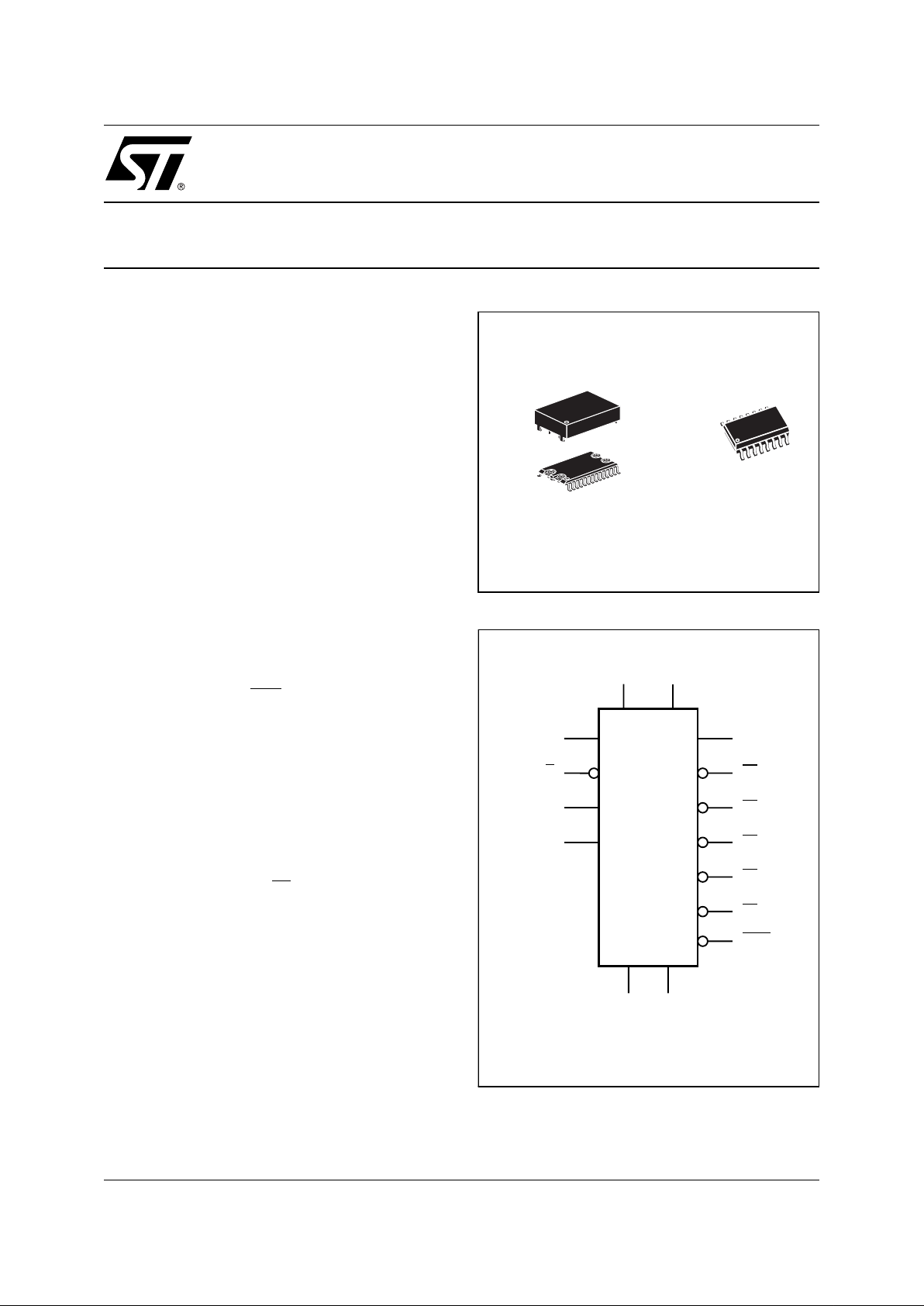
■ PACKAGING INCL UD ES a 28-L EAD SOI C
and SNAPHAT
®
TOP, or a 16-LEAD SOIC
(to be Ordered Separately)
■ SOIC PACKAGE PROVIDES D IREC T
CONNECTION for a SNAPHAT TOP which
CONTAINS the BATTERY
■ BATTERY LOW PIN (BL)
DESCRIPTION
The M40Z300/W NVRAM Con troller is a self-contained device which converts a standard low-power SRAM into a non-volatile memory. A precision
voltage reference and comparator monitors the
V
CC
input for an out-of-tolerance condition.
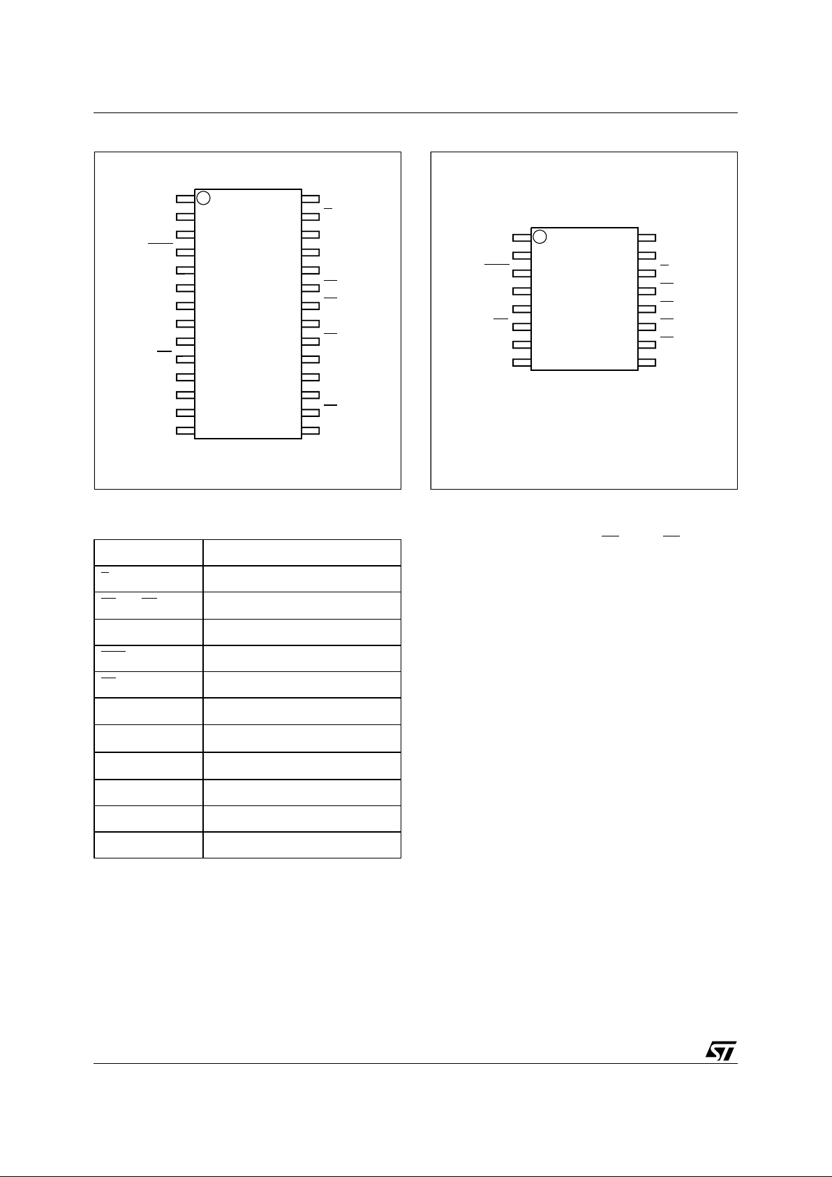
Figure 1. Logic Diagram
AI02242
THS
V
CC
M40Z300
M40Z300W
BL
V
SS
E
V
OUT
B
A
E1
CON
E2
CON
E3
CON
E4
CON
RST
B+
(1)
B–
(1)
NOTE: 1. For 16-pin SOIC package only.
28
1
SOH28 (MH)
SNAPHAT (SH)
Battery
16
1
SO16 (MQ)
Page 2
M40Z300, M40Z300W
2/16
When an invalid VCC condition occurs, t he conditioned chip enable outputs (E1
CON
to E4
CON
) are
forced inactive to write-protect the st ored data in
the SRAM. During a power failure, the SRAM is
switched from the V
CC
pin to the lithium cell within
the SNAPHAT to provide the energy required for
data retention. On a subsequent power-up, the
SRAM remains write protect ed until a valid power
condition returns.
The 28 pin, 330 mil SOIC provides sockets with
gold plated contacts for direct connection to a separate SNAPHAT housing containing the battery.
The SNAPHAT housing has gold plated pins
which mate with the sockets, ensuring reliable
connection. The housing is keyed to prevent improper insertion. This unique design allows the
SNAPHAT battery p acka ge t o b e m ount ed o n t op
of the SOIC package after the c ompletion of the
surface mount process which greatly reduces the
board manufacturing process complexity of either
directly soldering or inserting a battery into a soldered holder. Providing non-volatility becomes a
"SNAP".
The 16 pin SOIC provides battery pins for an external user supplied battery.
Figure 2A. SOIC28 Connections
AI02243
8
2
3
4
5
6
7
9
10
11
12
13
14
22
21
20
19
18
17
16
15
28
27
26
25
24
23
1
NC
NC
BL
NC
A
NC
B
RST
NC
NC
NC
E1
CON
NC
E3
CON
E
E2
CON
NC
NC
NCNC
THS
NCV
SS
E4
CON
NC
NC
V
OUT
V
CC
M40Z300
M40Z300W
Table 1. Signal Names
THS Threshold Select Input
E
Chip Enable Input
E1
CON
-E4
CON
Conditioned Chip Enable Output
A, B Decoder Inputs
RST
Reset Output (Open Drain)
BL
Battery Low Output (Open Drain)
V
OUT
Supply Voltage Output
V
CC
Supply Voltage
V
SS
Ground
B+ Positive Battery Pin
B– Negative Battery Pin
NC Not Connected Internally
Figure 2B. SOIC16 Connections
AI03624
8
2
3
4
5
6
710
16
15
14
13
12
11
1
A
RST
B
E1
CON
E
E2
CON
B– (B+)V
SS
NC
V
OUT
V
CC
M40Z300
M40Z300W
BL
THS
E3
CON
E4
CON
9
B+ (B–)
( ) = M40Z300W
Page 3

3/16
M40Z300, M40Z300W
Table 2. Absolute Maximum Ratings
(1)
Note: 1. Stresses greater than those listed under "Absolute Maximum Ratings" may cause permanent damage to the device. This is a stress
rating only and functional opera tion of the devi ce at these or any other conditions above thos e i ndi cated in th e operational section
of this spec ification is not im plied. Exposure t o the abso lute max imum rat ing cond itions for extende d period s of tim e may affe ct
reliability.
CAUTION: Negative undershoots below –0. 3V are not allowe d on any pin while i n the Battery Back-up mode.
CAUTION: Do NOT wave solder SOIC to avoid damaging SNAPHAT sockets.
Symbol Parameter Value Unit
T
A
Ambient Operating Temperature 0 to 70 °C
T
STG
Storage Temperature (VCC Off) SNAPHAT
SOIC
–40 to 85
–55 to 125
°C
V
IO
Input or Output Voltages
–0.3 to V
CC
+0.3
V
V
CC
Supply Voltage M40Z300
M40Z300W
–0.3 to 7
–0.3 to 4.6
V
I
O
Output Current 20 mA
P
D
Power Dissipation 1 W
OPERATION
The M40Z300/W, as shown in Figure 4, can c ontrol up to four (eight, if placed in parallel) standard
low-power SRAMs. These SRAMs must be configured to have the chip enable input disable all other
input signals. Most slow, low-power SRAMs are
configured like this, however many fast SRAMs
are not. During normal operating conditions, the
conditioned chip enable (E1
CON
to E4
CON
) output
pins follow the chip enable (E
) input pin with timing
shown in Table 7. An internal switch connects V
CC
to V
OUT
.
This switch has a vol tage drop of less than 0.3V
(I
OUT1
).
When V
CC
degrades during a power failure,
E1
CON
to E4
CON
are forced inactive inde pendent
of E
. In this situation, the SRAM is unconditionally
write protected as V
CC
falls below an out-of-toler-
ance threshold (V
PFD
). For the M40Z300 the pow-
er fail detection value associated with V
PFD
is
selected by the Threshold Select (THS) pin and is
shown in Table 6A. For the M 40Z300W, the THS
pin selects both the supply vo ltage and V
PFD
as
shown in Table 6B.
Note: In either case, THS pi n must b e connected
to either V
SS
or V
OUT
.
If chip enable access is in progress during a power
fail detection, that memory cycle continues to completion before the memory is write protected. I f the
memory cycle is not terminated within time t
WPT
,
E1
CON
to E4
CON
are unconditionally driven high,
write protecting the SRAM. A power failure during
a write cycle may corrupt data at the currently addressed location, but does not jeopardize the rest
of the SRAM’s contents. At voltages below V
PFD
(min), the user can be assured the memory will be
write protected within the Write Protect Time
(t
WPT
) provided the VCC fall time exceeds tF (See
Table 7).
As V
CC
continues to degrade, the internal switch
disconnects V
CC
and connects the internal battery
to V
OUT
. This occurs at the switchover voltage
(V
SO
). Below the VSO, the battery provides a volt-
age V
OHB
to the SRAM and can supply current
I
OUT2
(see Table 6A/6B).
When V
CC
rises above VSO, V
OUT
is switched
back to the supply voltage. Outputs E1
CON
to
E4
CON
are held inactive for t
CER
(120ms maxi-
mum) after the power supply has reached V
PFD
,
independent of the E
input, to all ow fo r proces sor
stabilization (see Figure 6).
Page 4
M40Z300, M40Z300W
4/16
DATA RETENTION LIFETIME CALCULATION
Most low power SRAMs on the market today can
be used with the M40Z300/W NVRAM Cont roller.
There are, however some criteria which should be
used in making the final choice of which S RA M to
use. The SRAM must be designed in a way where
the chip enable input disables all other inputs to
the SRAM. This allows i nputs to the M40Z 300/W
and SRAMs to be Don’t Care once V
CC
falls below
V
PFD
(min). The SRAM should also guarantee
data retention down to V
CC
= 2.0V. T he chip enable access time must be sufficient to meet the
system needs with the chip enable propagation
delays included. If the SRAM includes a second
Chip Enable pin (E2), this pin should be tied to
V
OUT
.
If data retention lifetime is a critical parameter f or
the system, it is importa nt to re view the dat a retention current specifications for the particular
SRAMs being evaluated. M ost SRAMs specify a
data retention current at 3.0V. Manufacturers generally specify a typical condition for room temperature along with a worst case condition (generally
at elevated temperatures). The system level requirements will determine the choice of which value to use. The data retent ion current val ue of the
SRAMs can then be added to t he I
CCDR
value of
the M40Z300/W to de termine the t otal current requirements for data retention. The available battery capacity for the SNAPHAT of your choice can
then be divided b y this current to determine the
amount of data retention available (see Table 8).
CAUTION: Take care to avoid inadvertent discharge through V
OUT
and E1
CON
-E4
CON
after bat-
tery has been attached.
For a further more detailed review of lifetime cal-
culations, please see Application Note AN1012.
Tabl e 3. Truth Table
Inputs Outputs
E
BA
E1
CON
E2
CON
E3
CON
E4
CON
HXXHHHH
LLLLHHH
LLHHLHH
LHLHHLH
LHHHHHL
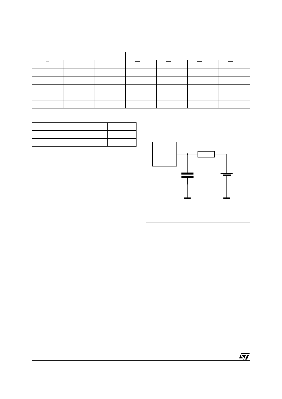
Figure 3. AC Testing Load Circuit
AI02393
CL = 50pF
CL includes JIG capacitance
333Ω
DEVICE
UNDER
TEST
1.73V
Table 4. AC Measurement Conditions
Input Rise and Fall Times ≤ 5ns
Input Pulse Voltages 0 to 3V
Input and Output Timing Ref. Voltages 1.5V
Page 5
5/16
M40Z300, M40Z300W
POWER-ON RESET OUTPUT
All microprocessors have a reset input which forces them to a known state when starting. The
M40Z300/W has a reset output (RST
) pin which is
guaranteed to be low within t
WPT
of V
PFD
(See Table 7). This signal is an open drain conf iguration.
An appropriate pull-up resistor should be chosen
to control the rise time. This signal will be valid for
all voltage conditions, even when V
CC
equals VSS.
Once V
CC
exceeds the power failure detect volt-
age V
PFD
, an internal timer keeps RST low for
t
REC
to allow the power supply to stabilize.
TWO TO FOUR DECODE
The M40Z300/W includes a 2 input (A, B) decoder
which allows the control of up to 4 independent
SRAMs. The Truth Table for these inputs is shown
in Table 3.
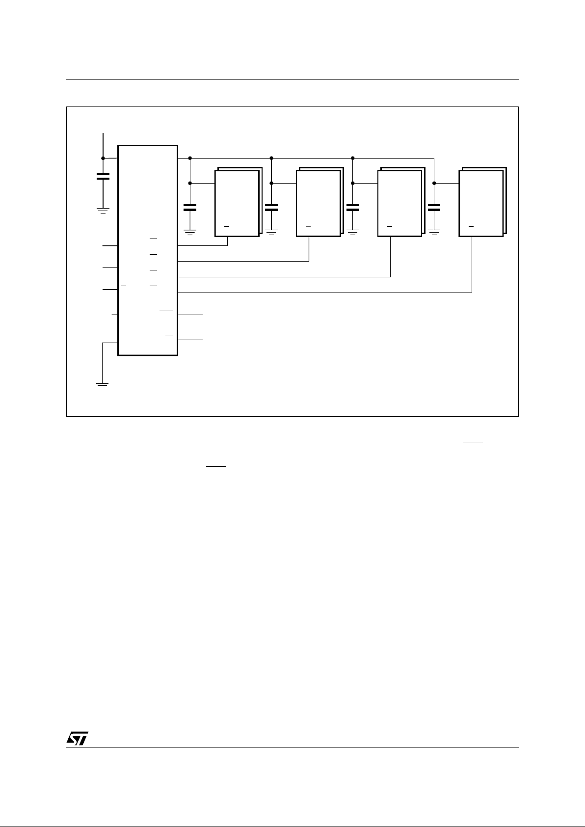
Figure 4. Hardware Hookup
AI02395
V
CC
E
E1
CON
V
SS
V
OUT
V
CC
CMOS
SRAM
3.0V, 3.3V or 5V
THS
A
0.1µF
0.1µF
M40Z300
M40Z300W
Threshold
E
B
E2
CON
E3
CON
E4
CON
RST
BL
E
V
CC
CMOS
SRAM
0.1µF
E
V
CC
CMOS
SRAM
0.1µF
E
V
CC
CMOS
SRAM
0.1µF
To Microprocessor
To Battery Monitor Circuit
Page 6

M40Z300, M40Z300W
6/16
Table 5. Capacitance
(1)
(T
A
= 25 °C, f = 1 MHz)
Note: 1. Sampled only, not 100% tested.
2. Outputs desele ct ed.
Table 6A. DC Characteristics for M40Z300
(T
A
= 0 to 70°C; VCC = 4.75V to 5.5V or 4.5V to 5.5V)
Note: 1. Outputs deselected.
2. For R ST
& BL pins (Open Drain).
3. Chip Enable outputs (E1
CON
- E4
CON
) can only s ustain CMO S leakage currents in th e battery back-up mode.
Higher leakage currents will reduce battery life.
4. Measured with V
OUT
and E1
CON
- E4
CON
open.
Symbol Parameter Test Condition Min Max Unit
C
IN
Input Capacitance
V
IN
= 0V
8pF
C
OUT
Output Capacitance
V
OUT
= 0V
10 pF
Symbol Parameter Test Condition Min Typ Max Unit
I
LI
(1)
Input Leakage Current
0V ≤ V
IN
≤ V
CC
±1 µA
I
CC
Supply Current Outputs open 3 6 mA
V
IL
Input Low Voltage –0.3 0.8 V
V
IH
Input High Voltage 2.2
V
CC
+ 0.3
V
V
OL
Output Low Voltage
I
OL
= 4.0mA
0.4 V
Output Low Voltage (open drain)
(2)
IOL = 10mA
0.4 V
V
OH
Output High Voltage
I
OH
= –2.0mA
2.4 V
V
OHB
VOH Battery Back-up
(3)
I
OUT2
= –1.0µA
2.0 2.9 3.6 V
I
OUT1
V
OUT
Current (Active)
V
OUT
> VCC –0.3
250 mA
V
OUT
> VCC –0.2
150 mA
I
OUT2
V
OUT
Current (Battery Back-up) V
OUT
> V
BAT
–0.3
100 µA
I
CCDR
Data Retention Mode Current
(4)
100 nA
THS Threshold Select Voltage
V
SS
V
OUT
V
V
PFD
Power-fail Deselect Voltage (THS = VSS)
4.5 4.6 4.75 V
Power-fail Deselect Voltage (THS = V
OUT
)
4.2 4.35 4.5 V
V
SO
Battery Back-up Switchover Voltage 3.0 V
Page 7

7/16
M40Z300, M40Z300W
Table 6B. DC Characteristics for M40Z300W
(T
A
= 0 to 70°C; VCC = 3V to 3.6V or 2.7V to 3.3V)
Note: 1. Outputs deselected.
2. For R ST
& BL pins (Open Drain).
3. Chip Enable outputs (E1
CON
- E4
CON
) can only s ustain CMO S leakage currents in th e battery back-up mode.
Higher leakage currents will reduce battery life.
4. Measured with V
OUT
and E1
CON
- E4
CON
open.
Symbol Parameter Test Condition Min Typ Max Unit
I
LI
(1)
Input Leakage Current
0V ≤ V
IN
≤ V
CC
±1 µA
I
CC
Supply Current Outputs open 2 4 mA
V
IL
Input Low Voltage –0.3 0.8 V
V
IH
Input High Voltage 2.0
V
CC
+ 0.3
V
V
OL
Output Low Voltage
I
OL
= 4.0mA
0.4 V
Output Low Voltage (open drain)
(2)
IOL = 10mA
0.4 V
V
OH
Output High Voltage
I
OH
= –2.0mA
2.4 V
V
OHB
VOH Battery Back-up
(3)
I
OUT2
= –1.0µA
2.0 2.9 3.6 V
I
OUT1
V
OUT
Current (Active)
V
OUT
> VCC –0.3
150 mA
V
OUT
> VCC –0.2
100 mA
I
OUT2
V
OUT
Current (Battery Back-up) V
OUT
> V
BAT
–0.3
100 µA
I
CCDR
Data Retention Mode Current
(4)
100 nA
THS Threshold Select Voltage
V
SS
V
OUT
V
V
PFD
Power-fail Deselect Voltage (THS = VSS)
2.8 2.9 3.0 V
Power-fail Deselect Voltage (THS = V
OUT
)
2.5 2.6 2.7 V
V
SO
Battery Back-up Switchover Voltage 2.5 V
Page 8

M40Z300, M40Z300W
8/16
Table 7. Power Down/Up AC Characteristics
(T
A
= 0 to 70°C)
Note: 1. V
PFD
(max) to V
PFD
(min) fall ti me of less than t F m ay result in deselection/ write prote ct i on not occurri ng until 200 µs af ter
V
CC
passes V
PFD
(min)..
2. V
PFD
(min) to VSS fall time of le ss than tFB may cause corrup tion of RAM dat a.
Symbol Parameter Min Max Unit
t
F
(1)
V
PFD
(max) to V
PFD
(min) VCC Fall Time
300 µs
t
FB
(2)
V
PFD
(min) to VSS VCC Fall Time
150 µs
t
R
V
PFD
(min) to V
PFD
(max) VCC Rise Time
10 µs
t
EDL
Chip Enable Propagation Delay Low
M40Z300 12 ns
M40Z300W 20 ns
t
EDH
Chip Enable Propagation Delay High
M40Z300 10 ns
M40Z300W 20 ns
t
AS
A, B set up to E 0ns
t
CER
Chip Enable Recovery 40 120 ms
t
REC
V
PFD
(max) to RST High
40 120 ms
t
WPT
Write Protect Time
M40Z300 40 150 µs
M40Z300W 40 250 µs
t
RB
VSS to V
PFD
(min) VCC Rise Time
1µs
BATTERY LOW PIN
The M40Z300/W automatically performs battery
voltage monitoring upon power-up, and at factoryprogrammed time intervals of at least 24 hours.
The Battery Low (BL
) pin will be a sserted if the
battery voltage is f ound to be less than approximately 2.5V. The BL
pin will remain asserted until
completion of battery replacement and subsequent battery low monitoring tests, either during
the next power-up sequence or the next scheduled
24-hour interval.
If a battery low is generated during a power-up sequence, this indicates that the battery is below
2.5V and may not be able to maintain data integrity
in the SRAM. Data should be considered suspect,
and verified as correct. A fresh battery should be
installed.
If a battery low indication is generated during the
24-hour interval check, this indicates that the battery is near end of life. However, data is not compromised due to the fact that a nominal V
CC
is
supplied. In order to insure data integrity during
subsequent periods of bat tery back-up m ode, the
battery should be replaced. SNAPHAT top should
be replaced with valid V
CC
applied to the device.
The M40Z300/W only monitors the battery when a
nominal V
CC
is applied to the device. Thus applications which require extensive durations in the
battery back-up mode should be powered-up periodically (at least once every few months) in order
for this technique to be beneficial. Additionally, if a
battery low is indicated, data integrity should be
verified upon power-up via a checksum or other
technique. The BL
pin is an open drain output and
an appropriate pull-up resistor to V
CC
should be
chosen to control the rise time.
Page 9

9/16
M40Z300, M40Z300W
Figure 5. Power Down Timing
Figure 6. Power Up Timing
AI02398B
V
CC
E
E1
CON
-
E4
CON
tF
tFB
V
OHB
V
PFD
(max)
V
PFD
(min)
VSO
tWPT
V
PFD
RST
AI02399B
V
CC
E
E1
CON
-
E4
CON
tR
tCER
V
OHB
V
PFD
(max)
V
PFD
(min)
VSO
V
PFD
tEDLtEDH
RST
tREC
tRB
Page 10

M40Z300, M40Z300W
10/16
VCC NOISE AND NEGATIVE GOING TRANSIENTS
I
CC
transients, including those produced by output
switching, can produce voltage fluctuations, resulting in spikes on the V
CC
bus. These transients
can be reduced if capacitors are used to store energy, which stabilizes the V
CC
bus. The energy
stored in the bypass capacitors will be released as
low going spikes are generated or energy will be
absorbed when overshoots occur.
A ceramic bypass capacitor value of 0.1µF (as
shown in figure 8) is recommended in order to provide the needed filtering.
In addition to transients that are caused by normal
SRAM operation, power cycling can generate negative voltage spikes on V
CC
that drive it to values
below V
SS
by as much as one volt. These negative
spikes can cause data corruption in the SRAM
while in battery backup mode. To protect from
these voltage spikes, STMicroelectronics recommends connecting a schottky diode from V
CC
to
V
SS
(cathode connected to VCC, anode to VSS).
Schottky diode 1N5817 is recommended for
through hole and MBRS120T3 is recommended
for surface mount.
Figure 7. Address-Decode Time
Note: During sys tem design , c om pl i ance with th e SRAM timin g parameters must comprehend the p ropagation delay
between E
and EX
CON
AI02551
A, B
E
E1
CON
-E4
CON
tAS
tEDH or tEDL
tEDL
Figure 8. Supply Voltage Protection
AI00622
V
CC
0.1µF DEVICE
V
CC
V
SS
Table 8. Battery Table
Part Number Description Package
M4Z28-BR00SH Lithium Battery (48mAh) SNAPHAT SH
M4Z32-BR00SH Lithium Battery (120mAh) SNAPHAT SH
Page 11

11/16
M40Z300, M40Z300W
Table 9. Ordering Information Scheme
Note: 1. The SOIC pack age (SOH28) requires the battery package (SNA PHAT) whic h i s ordered sep arately under the part num ber
“M4Zxx-B R00SH1" in pl astic tube or " M 4Z xx-BR00SH1TR" in Ta pe & Reel form.
2. Delivery may include either the 2-pin version of the SOIC/SNAPHAT or the 4-pin version of the SOIC/SNAPHAT. Both are functionally equival ent (see package drawing section f or details).
Caution: Do not place the SNAPHAT bat tery package "M4Zxx-BR0 0SH1" in conduct ive foam since will dr ain th e lithium b utton-cell battery.
For a list of available options (Speed, Pac kage, etc...) or for furthe r information on any aspect of this device, please contact the ST Sales Office nearest to you.
Example: M40Z300W MH 1 TR
Supply Voltage and Write Protect Voltage
300 = V
CC
= 4.5V to 5.5V
THS = V
SS
4.5V ≤ V
PFD
≤ 4.75V
THS = V
OUT
4.2V ≤ V
PFD
≤ 4.5V
300W = V
CC
= 3.0V to 3.6V
THS = V
SS
2.8V ≤ V
PFD
≤ 3.0V
V
CC
= 2.7V to 3.3V
THS = V
OUT
2.5V ≤ V
PFD
≤ 2.7V
Package
MH
(1,2)
= SOH28
MQ = SO16
Temperature Range
1 = 0 to 70 °C
Shipping Method for SOIC
blank = Tubes
TR = Tape & Reel
Table 10. Revision History
Date Revision Details
March 1999 First Issue
03/08/00
Document Layout changed
SO16 package added
Battery Capacity changed (Table 8)
Page 12

M40Z300, M40Z300W
12/16
Table 11. SOH28 - 28 l ead Plastic Small Outl ine, battery S NAPHAT, Package M echanical Data
Symb
mm inches
Typ Min Max Typ Min Max
A 3.05 0.120
A1 0.05 0.36 0.002 0.014
A2 2.34 2.69 0.092 0.106
B 0.36 0.51 0.014 0.020
C 0.15 0.32 0.006 0.012
D 17.71 18.49 0.697 0.728
E 8.23 8.89 0.324 0.350
e 1.27 – – 0.050 – –
eB 3.20 3.61 0.126 0.142
H 11.51 12.70 0.453 0.500
L 0.41 1.27 0.016 0.050
α 0° 8° 0° 8°
N 28 28
CP 0.10 0.004
Figure 9. SOH28 - 28 lead Plastic Small Outline, 4-socket battery SNAPHAT, Package Outline
Drawing is not to scale.
SOH-A
E
N
D
C
LA1 α
1
H
A
CP
Be
A2
eB
Page 13

13/16
M40Z300, M40Z300W
Table 12. M4Z28-BR00SH SNAPHAT Housing for 48 mAh Battery, Package Mechanical Data
Symb
mm inches
Typ Min Max Typ Min Max
A 9.78 0.385
A1 6.73 7.24 0.265 0.285
A2 6.48 6.99 0.255 0.275
A3 0.38 0.015
B 0.46 0.56 0.018 0.022
D 21.21 21.84 0. 835 0.860
E 14.22 14.9 9 0.560 0.590
eA 15.55 15.9 5 0.612 0.628
eB 3.20 3.61 0.126 0.142
L 2.03 2.29 0.080 0.090
Figure 10. M4Z28-BR00SH SNAPHAT Housin g f or 48 mAh Batte ry, Package Outline
Drawing is not to scale.
SHZP-A
A1
A
D
E
eA
eB
A2
B
L
A3
Page 14

M40Z300, M40Z300W
14/16
Table 13. M4Z32-BR00SH SNAPHAT Housing for 120 mAh Battery, Package Mechanical Data
Symb
mm inches
Typ Min Max Typ Min Max
A 10.5 4 0.415
A1 8.00 8.51 0.315 .0335
A2 7.24 8.00 0.285 0.315
A3 0.38 0.015
B 0.46 0.56 0.018 0.022
D 21.21 21.84 0. 835 0.860
E 17.27 18.0 3 0.680 .0710
eA 15.55 15.9 5 0.612 0.628
eB 3.20 3.61 0.126 0.142
L 2.03 2.29 0.080 0.090
Figure 11. M4Z32-BR 00SH S NAPHAT Hous ing for 120 mAh Batte ry, Package Outline
Drawing is not to scale.
SHZP-A
A1
A
D
E
eA
eB
A2
B
L
A3
Page 15

15/16
M40Z300, M40Z300W
Table 14. SO16 - 16 lead Plastic Small Outline, 300 mils body width
Symb.
mm inches
Typ. Min. Max. Typ. Min. Ma x.
A 2.59 0.102
A1 0.10 0.30 0.004 0.012
B 0.38 0.51 0.015 0.020
C 0.23 0.25 0.009 0.010
D 10.11 10.49 0.398 0.413
E 7.44 7.54 0.293 0.297
e 1.27 – – 0.050 – –
H 10.16 10.41 0.400 0.410
h 0.38 0. 015
L 0.41 1027 0.016 0.050
α 0° 8° 0° 8°
N16 16
CP 0.10 0.0 04
Figure 12. SO16 - 16 lead Plastic Small Outline, 300 mils body width, Package Outline
Drawing is not to scale.
SO-a
E
N
CP
B
e
A
D
C
LA1 α
1
H
h x 45˚
Page 16

M40Z300, M40Z300W
16/16
Information furnished is believed to be ac curate and reli able. Howev er, STMicroel ectronics assumes no resp onsibility for the cons equences
of use of such information nor for any infringement of patents or other rights of third parties which may result from its use. No license is granted
by implic ation or otherwise under any patent or patent rights of STMi croelectr onics. Specifications menti oned in thi s publicati on are subject
to change without notice. This publication supersedes and replaces all information previously supplied. STMicroelectronics products are not
authorized for use as cri tical comp onents in life support dev i ces or systems wi thout express written approval of STMicroel ectronics.
The ST log o i s registered trademark of STMicroelectronics
2000 STMicroel e ctronics - All Rights Re served
All other names are the property of their resp ective owner s.
STMicroelect ro n ics GRO UP OF COMPANI ES
Australi a - Brazil - Chi na - Finland - F rance - Germ any - Hong Kong - India - Ital y - Japan - Ma la ys i a - M al ta - Morocco -
Singapor e - Spain - Sweden - Switzerl and - United Kingdom - U.S.A.
http://www.st.com
 Loading...