

Page 1
M40SZ100Y
M40SZ100W
5 V or 3 V NVRAM supervisor for LPSRAM
Features
■ Convert low power SRAMs into NVRAMs
■ 5 V or 3 V operating voltage
■ Precision power monitoring and power
switching circuitry
■ Automatic write-protection when V
tolerance
■ Choice of supply voltages and power-fail
deselect voltages:
– M40SZ100Y: V
4.20 V ≤ V
PFD
= 4.5 to 5.5 V;
CC
≤ 4.50 V
(contact local ST sales office for
availability)
– M40SZ100W: V
2.55 V ≤ V
■ Reset output (RST) for power on reset
■ 1.25 V reference (for PFI/PFO)
■ Less than 10 ns chip enable access
PFD
= 2.7 to 3.6 V;
CC
≤ 2.70 V
propagation delay (at 5 V)
■ Optional packaging includes a 28-lead SOIC
and SNAPHAT
■ 28-lead SOIC package provides direct
®
top (to be ordered separately)
connection for a SNAPHAT top which contains
the battery (contact local ST sales office for
availability)
■ Battery low pin (BL)
■ RoHS compliant
– Lead-free second level interconnect
is out-of-
CC
16
1
SO16 (MQ)
SNAPHAT (SH) battery
28
1
SOH28 (MH)
October 2010 Doc ID 7528 Rev 3 1/24
www.st.com
1
Page 2

Contents M40SZ100Y, M40SZ100W
Contents
1 Description . . . . . . . . . . . . . . . . . . . . . . . . . . . . . . . . . . . . . . . . . . . . . . . . . 5
2 Operation . . . . . . . . . . . . . . . . . . . . . . . . . . . . . . . . . . . . . . . . . . . . . . . . . . 9
2.1 Data retention lifetime calculation . . . . . . . . . . . . . . . . . . . . . . . . . . . . . . . 9
2.2 Power-on reset output . . . . . . . . . . . . . . . . . . . . . . . . . . . . . . . . . . . . . . . 12
2.3 Reset input (RSTIN
2.4 Battery low pin . . . . . . . . . . . . . . . . . . . . . . . . . . . . . . . . . . . . . . . . . . . . . 12
2.5 Power-fail input/output . . . . . . . . . . . . . . . . . . . . . . . . . . . . . . . . . . . . . . . 13
2.6 V
noise and negative going transients . . . . . . . . . . . . . . . . . . . . . . . . . 13
CC
) . . . . . . . . . . . . . . . . . . . . . . . . . . . . . . . . . . . . . . . . . 12
3 Maximum ratings . . . . . . . . . . . . . . . . . . . . . . . . . . . . . . . . . . . . . . . . . . . 15
4 DC and AC parameters . . . . . . . . . . . . . . . . . . . . . . . . . . . . . . . . . . . . . . 16
5 Package mechanical data . . . . . . . . . . . . . . . . . . . . . . . . . . . . . . . . . . . . 18
6 Part numbering . . . . . . . . . . . . . . . . . . . . . . . . . . . . . . . . . . . . . . . . . . . . 22
7 Revision history . . . . . . . . . . . . . . . . . . . . . . . . . . . . . . . . . . . . . . . . . . . 23
2/24 Doc ID 7528 Rev 3
Page 3

M40SZ100Y, M40SZ100W List of tables
List of tables
Table 1. Signal names . . . . . . . . . . . . . . . . . . . . . . . . . . . . . . . . . . . . . . . . . . . . . . . . . . . . . . . . . . . . 6
Table 2. Power down/up AC characteristics . . . . . . . . . . . . . . . . . . . . . . . . . . . . . . . . . . . . . . . . . . . 11
Table 3. Reset AC characteristics . . . . . . . . . . . . . . . . . . . . . . . . . . . . . . . . . . . . . . . . . . . . . . . . . . 12
Table 4. Absolute maximum ratings . . . . . . . . . . . . . . . . . . . . . . . . . . . . . . . . . . . . . . . . . . . . . . . . . 15
Table 5. DC and AC measurement conditions . . . . . . . . . . . . . . . . . . . . . . . . . . . . . . . . . . . . . . . . . 16
Table 6. Capacitance . . . . . . . . . . . . . . . . . . . . . . . . . . . . . . . . . . . . . . . . . . . . . . . . . . . . . . . . . . . . 16
Table 7. DC characteristics. . . . . . . . . . . . . . . . . . . . . . . . . . . . . . . . . . . . . . . . . . . . . . . . . . . . . . . . 17
Table 8. SO16 – 16-lead plastic small outline package mechanical data. . . . . . . . . . . . . . . . . . . . . 18
Table 9. SOH28 – 28-lead plastic small outline, battery SNAPHAT, pack. mech. data . . . . . . . . . . 19
Table 10. SH – 4-pin SNAPHAT housing for 48 mAh battery, package mechanical data . . . . . . . . . 20
Table 11. SH – 4-pin SNAPHAT housing for 120 mAh battery, package mechanical data . . . . . . . . 21
Table 12. Ordering information scheme . . . . . . . . . . . . . . . . . . . . . . . . . . . . . . . . . . . . . . . . . . . . . . . 22
Table 13. SNAPHAT
Table 14. Document revision history . . . . . . . . . . . . . . . . . . . . . . . . . . . . . . . . . . . . . . . . . . . . . . . . . 23
®
battery table . . . . . . . . . . . . . . . . . . . . . . . . . . . . . . . . . . . . . . . . . . . . . . . . . . 22
Doc ID 7528 Rev 3 3/24
Page 4

List of figures M40SZ100Y, M40SZ100W
List of figures
Figure 1. Logic diagram . . . . . . . . . . . . . . . . . . . . . . . . . . . . . . . . . . . . . . . . . . . . . . . . . . . . . . . . . . . . 5
Figure 2. SOIC16 connections . . . . . . . . . . . . . . . . . . . . . . . . . . . . . . . . . . . . . . . . . . . . . . . . . . . . . . . 6
Figure 3. SOIC28 connections . . . . . . . . . . . . . . . . . . . . . . . . . . . . . . . . . . . . . . . . . . . . . . . . . . . . . . . 7
Figure 4. Block diagram . . . . . . . . . . . . . . . . . . . . . . . . . . . . . . . . . . . . . . . . . . . . . . . . . . . . . . . . . . . . 7
Figure 5. Hardware hookup . . . . . . . . . . . . . . . . . . . . . . . . . . . . . . . . . . . . . . . . . . . . . . . . . . . . . . . . . 8
Figure 6. Power down timing . . . . . . . . . . . . . . . . . . . . . . . . . . . . . . . . . . . . . . . . . . . . . . . . . . . . . . . 10
Figure 7. Power up timing . . . . . . . . . . . . . . . . . . . . . . . . . . . . . . . . . . . . . . . . . . . . . . . . . . . . . . . . . 11
Figure 8. RSTIN
Figure 9. Supply voltage protection . . . . . . . . . . . . . . . . . . . . . . . . . . . . . . . . . . . . . . . . . . . . . . . . . . 14
Figure 10. AC testing load circuit . . . . . . . . . . . . . . . . . . . . . . . . . . . . . . . . . . . . . . . . . . . . . . . . . . . . . 16
Figure 11. AC testing input/output waveforms . . . . . . . . . . . . . . . . . . . . . . . . . . . . . . . . . . . . . . . . . . . 16
Figure 12. SO16 – 16-lead plastic small package outline . . . . . . . . . . . . . . . . . . . . . . . . . . . . . . . . . . 18
Figure 13. SOH28 – 28-lead plastic small outline, 4-socket battery SNAPHAT, package outline . . . . 19
Figure 14. SH – 4-pin SNAPHAT housing for 48 mAh battery, package outline . . . . . . . . . . . . . . . . . 20
Figure 15. SH – 4-pin SNAPHAT housing for 120 mAh battery, package outline . . . . . . . . . . . . . . . . 21
timing waveform . . . . . . . . . . . . . . . . . . . . . . . . . . . . . . . . . . . . . . . . . . . . . . . . . . . 12
4/24 Doc ID 7528 Rev 3
Page 5
M40SZ100Y, M40SZ100W Description
1 Description
The M40SZ100Y/W NVRAM controller is a self-contained device which converts a standard
low-power SRAM into a non-volatile memory. A precision voltage reference and comparator
monitors the V
When an invalid V
inactive to write protect the stored data in the SRAM. During a power failure, the SRAM is
switched from the V
the 16-lead SOIC) to provide the energy required for data retention. On a subsequent
power-up, the SRAM remains write protected until a valid power condition returns.
input for an out-of-tolerance condition.
CC
condition occurs, the conditioned chip enable output (E
CC
pin to the lithium cell within the SNAPHAT® (or external battery for
CC
) is forced
CON
The 28-pin, 330 mil SOIC provides sockets with gold plated contacts for direct connection to
a separate SNAPHAT
®
housing containing the battery. The SNAPHAT housing has gold
plated pins which mate with the sockets, ensuring reliable connection. The housing is keyed
to prevent improper insertion. This unique design allows the SNAPHAT battery package to
be mounted on top of the SOIC package after the completion of the surface mount process
which greatly reduces the board manufacturing process complexity of either directly
soldering or inserting a battery into a soldered holder. Providing non-volatility becomes a
“SNAP.” This feature is also available in the “topless” 16-pin SOIC package (MQ).
Insertion of the SNAPHAT housing after reflow prevents potential battery damage due to the
high temperatures required for device surface-mounting. The SNAPHAT housing is also
keyed to prevent reverse insertion.
The 28-pin SOIC and battery packages are shipped separately in plastic anti-static tubes or
in tape & reel form. For the 28-lead SOIC, the battery/crystal package (e.g., SNAPHAT) part
number is M4Z28-BR00SH (for 48 mAh battery)
or M4Z32-BR00SH (for 120 mAh battery).
Caution: Do not place the SNAPHAT battery top in conductive foam, as this will drain the lithium
button-cell battery.
Figure 1. Logic diagram
(1)
V
V
CC
BAT
RSTIN
1. For 16-pin SOIC package only.
V
OUT
E
PFI
Doc ID 7528 Rev 3 5/24
M40SZ100Y
M40SZ100W
V
SS
BL
E
CON
PFO
RST
AI03933
Page 6
Description M40SZ100Y, M40SZ100W
Table 1. Signal names
E Chip enable input
E
CON
Conditioned chip enable output
RST Reset output (open drain)
RSTIN Reset input
BL Battery low output (open drain)
V
V
V
BAT
OUT
CC
(1)
Supply voltage output
Supply voltage
Backup supply voltage
PFI Power fail input
PFO Power fail output
V
SS
Ground
NC Not connected internally
1. For SO16 only.
Figure 2. SOIC16 connections
NC
NC
RST
NC
RSTIN
PFO
V
BAT
V
SS
V
1
2
3
4
M40SZ100Y
M40SZ100W
5
6
710
8
16
15
14
13
12
11
CC
NC
V
OUT
NC
PFI
BL
E
9
E
CON
AI03935
6/24 Doc ID 7528 Rev 3
Page 7
M40SZ100Y, M40SZ100W Description
Figure 3. SOIC28 connections
Figure 4. Block diagram
V
CC
V
BAT
BL
NC
NC
NC
NC
NC
NC
NC
RSTIN
NC
NC
PFO
V
SS
VBL= 2.5V
1
2
3
4
5
6
7
M40SZ100Y
M40SZ100W
8
9
10
11
12
13
14
COMPARE
28
27
26
25
24
23
22
21
20
19
18
17
16
15
V
CC
NC
NC
V
OUT
NC
NC
PFI
NC
E
NC
RST
NCNC
NC
E
CON
V
BL
AI03934
OUT
(1)
RSTIN
E
PFI
1.25V
1. Open drain output
V
V
PFD
= 2.5V
SO
= 4.4V
(2.65V for SZ100W)
COMPARE
COMPARE
COMPARE
POR
RST
E
CON
PFO
(1)
AI04766
Doc ID 7528 Rev 3 7/24
Page 8
Description M40SZ100Y, M40SZ100W
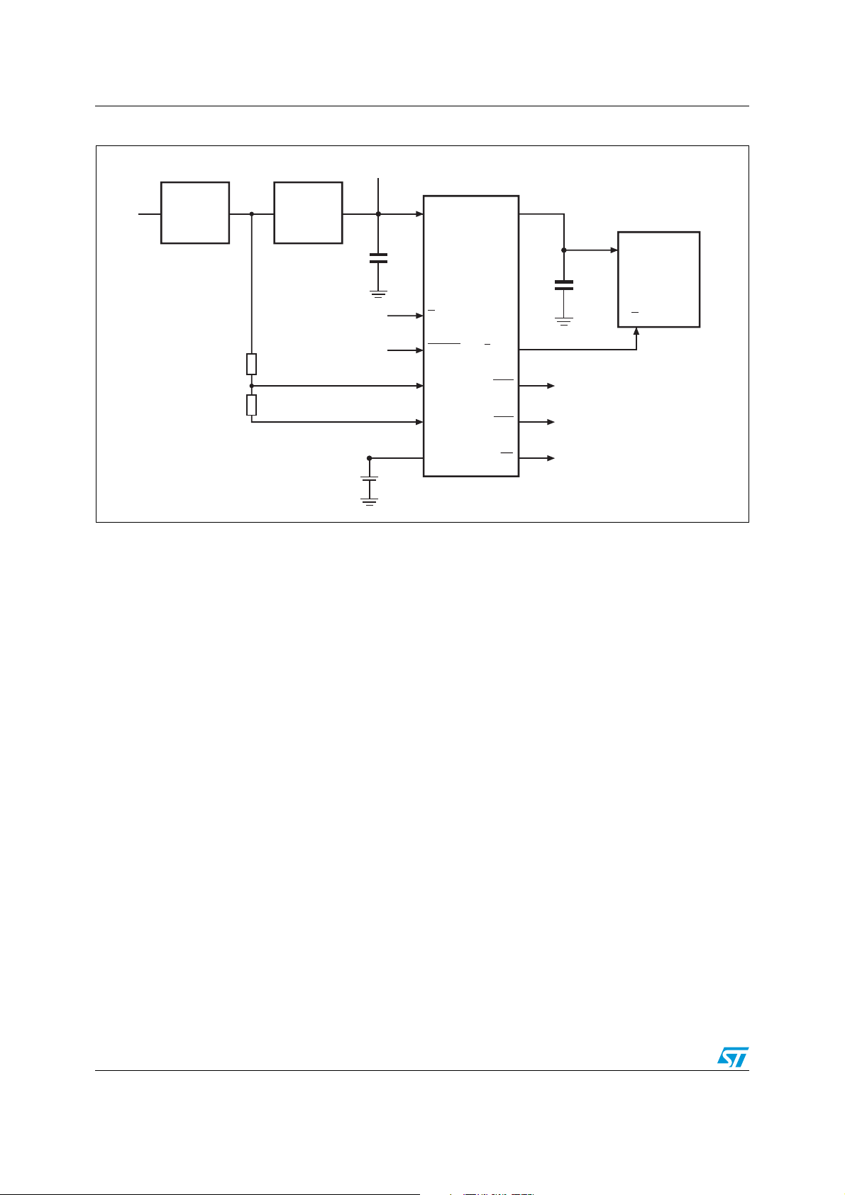
Figure 5. Hardware hookup
3.0V, 3.3V or 5V
Unregulated
Voltage
R1
R2
Regulator
V
IN
1. User supplied for the 16-pin package
V
CC
0.1µF
From Microprocessor
V
CC
E
RSTIN
PFI
V
SS
V
BAT
V
OUT
M40SZ100Y
M40SZ100W
E
CON
PFO
RST
(1)
BL
V
CC
0.1µF
To Microprocessor NMI
To Microprocessor Reset
To Battery Monitor Circuit
1Mb or 4Mb
LPSRAM
E
AI04767
8/24 Doc ID 7528 Rev 3
Page 9

M40SZ100Y, M40SZ100W Operation
2 Operation
The M40SZ100Y/W, as shown in Figure 5 on page 8, can control one (two, if placed in
parallel) standard low-power SRAM. This SRAM must be configured to have the chip enable
input disable all other input signals. Most slow, low-power SRAMs are configured like this,
however many fast SRAMs are not. During normal operating conditions, the conditioned
chip enable (E
Table2 on page11. An internal switch connects V
of less than 0.3 V (I
When V
degrades during a power failure, E
CC
situation, the SRAM is unconditionally write protected as V
threshold (V
V
is shown in Table 7 on page 17.
PFD
If chip enable access is in progress during a power fail detection, that memory cycle
continues to completion before the memory is write protected. If the memory cycle is not
terminated within time t
A power failure during a WRITE cycle may corrupt data at the currently addressed location,
but does not jeopardize the rest of the SRAM's contents. At voltages below V
user can be assured the memory will be write protected within the Write Protect Time (t
provided the V
As V
continues to degrade, the internal switch disconnects VCC and connects the internal
CC
battery to V
provides a voltage V
page 17).
) output pin follows the chip enable (E) input pin with timing shown in
CON
).
OUT1
). For the M40SZ100Y/W the power fail detection value associated with
PFD
, E
WPT
fall time does not exceed tF (see Table 2 on page 11).
CC
. This occurs at the switchover voltage (VSO). Below the VSO, the battery
OUT
to the SRAM and can supply current I
OHB
is unconditionally driven high, write protecting the SRAM.
CON
to V
CC
is forced inactive independent of E. In this
CON
. This switch has a voltage drop
OUT
falls below an out-of-tolerance
CC
PFD
(see Ta b le 7 o n
OUT2
(min), the
WPT
)
When V
held inactive for t
independent of the E
rises above VSO, V
CC
(120ms maximum) after the power supply has reached V
CER
input, to allow for processor stabilization (see Figure 7 on page 11).
is switched back to the supply voltage. Output E
OUT
2.1 Data retention lifetime calculation
Most low power SRAMs on the market today can be used with the M40SZ100Y/W NVRAM
Controller. There are, however some criteria which should be used in making the final
choice of which SRAM to use. The SRAM must be designed in a way where the chip enable
input disables all other inputs to the SRAM. This allows inputs to the M40SZ100Y/W and
SRAMs to be “Don't care” once V
SRAM should also guarantee data retention down to V
time must be sufficient to meet the system needs with the chip enable propagation delays
included.
If data retention lifetime is a critical parameter for the system, it is important to review the
data retention current specifications for the particular SRAMs being evaluated. Most SRAMs
specify a data retention current at 3.0 V. Manufacturers generally specify a typical condition
for room temperature along with a worst case condition (generally at elevated
temperatures). The system level requirements will determine the choice of which value to
use. The data retention current value of the SRAMs can then be added to the I
the M40SZ100Y/W to determine the total current requirements for data retention. The
available battery capacity for the SNAPHAT
then be divided by this current to determine the amount of data retention available.
falls below V
CC
®
of your choice (see Table 13 on page 22) can
PFD
(min) (see Figure 6 on page 10). The
PFD
= 2.0 V. The chip enable access
CC
CCDR
is
CON
,
value of
Doc ID 7528 Rev 3 9/24
Page 10

Operation M40SZ100Y, M40SZ100W
Caution: Take care to avoid inadvertent discharge through V
attached.
For a further more detailed review of lifetime calculations, please see application note
AN1012.
Figure 6. Power down timing
V
CC
V
(max)
PFD
V
PFD
V
(min)
PFD
VSO
tF
tFB
E
E
tWPT
CON
V
OHB
OUT
and E
after battery has been
CON
RST
PFO
VAL ID
AI03936
10/24 Doc ID 7528 Rev 3
Page 11

M40SZ100Y, M40SZ100W Operation
Figure 7. Power up timing
V
CC
V
(max)
PFD
V
PFD
V
(min)
PFD
VSO
tR
E
E
CON
RST
PFO
tRB
V
OHB
tCER
tEPDtEPD
tREC
VAL ID
Table 2. Power down/up AC characteristics
Symbol Parameter
(2)
t
F
t
FB
t
PFD
t
t
EPD
t
RB
t
CER
t
REC
t
WPT
1. Valid for ambient operating temperature: TA = –40 to 85 °C; VCC = 2.7 to 3.6 V or 4.5 to 5.5 V(except where noted).
2. V
PFD
V
CC
3. V
PFD
V
(3)
(max) to V
PFD
V
(min) to VSS VCC fall time 10 µs
PFD
(min) VCC fall time 300 µs
PFD
PFI to PFO propagation delay 15 25 µs
V
R
(min) to V
PFD
(max) VCC rise time 10 µs
PFD
Chip enable propagation delay (low or high)
VSS to V
(min) VCC rise time 1 µs
PFD
Chip enable recovery 40 120 ms
V
(max) to RST high 40 200 ms
PFD
Write protect time 40 200 µs
(max) to V
passes V
(min) to VSS fall time of less than tFB may cause corruption of RAM data.
(min) fall time of less than tF may result in deselection/write protection not occurring until 200 µs after
PFD
(min).
PFD
(1)
Min Max Unit
M40SZ100Y 10 ns
M40SZ100W 15 ns
AI03937
Doc ID 7528 Rev 3 11/24
Page 12

Operation M40SZ100Y, M40SZ100W
2.2 Power-on reset output
All microprocessors have a reset input which forces them to a known state when starting.
The M40SZ100Y/W has a reset output (RST
) pin which is guaranteed to be low by V
PFD
(see Table 7 on page 17). This signal is an open drain configuration. An appropriate pull-up
resistor to V
voltage conditions, even when V
Once V
for t
CC
to allow the power supply to stabilize.
REC
should be chosen to control the rise time. This signal will be valid for all
CC
exceeds the power failure detect voltage V
equals VSS (with valid battery voltage).
CC
, an internal timer keeps RST low
PFD
2.3 Reset input (RSTIN)
The M40SZ100Y/W provides one independent input which can generate an output reset.
The duration and function of this reset is identical to a reset generated by a power cycle.
Ta bl e 3 and Figure 8 illustrate the AC reset characteristics of this function. Pulses shorter
than t
100 kΩ resistor.
will not generate a reset condition. RSTIN is internally pulled up to VCC through a
RLRH
Figure 8. RSTIN
RSTIN
(1)
RST
1. With pull-up resistor
timing waveform
Table 3. Reset AC characteristics
Symbol Parameter
(2)
t
RLRH
(3)
t
R1HRH
1. Valid for ambient operating temperature: TA = –40 to 85 °C; VCC = 2.7 to 3.6 V or 4.5 to 5.5 V (except
where noted).
2. Pulse width less than 50 ns will result in no RESET (for noise immunity).
3. CL = 5 pF (see Figure 10 on page 16).
RSTIN low to RSTIN high 200 ns
RSTIN high to RST high 40 200 ms
2.4 Battery low pin
tRLRH
tR1HRH
(1)
AI04768
Min Max Unit
The M40SZ100Y/W automatically performs battery voltage monitoring upon power-up, and
at factory-programmed time intervals of at least 24 hours. The Battery Low (BL
asserted if the battery voltage is found to be less than approximately 2.5 V. The BL
remain asserted until completion of battery replacement and subsequent battery low
monitoring tests, either during the next power-up sequence or the next scheduled 24-hour
interval.
12/24 Doc ID 7528 Rev 3
) pin will be
pin will
Page 13

M40SZ100Y, M40SZ100W Operation
If a battery low is generated during a power-up sequence, this indicates that the battery is
below 2.5 V and may not be able to maintain data integrity in the SRAM. Data should be
considered suspect, and verified as correct. A fresh battery should be installed.
If a battery low indication is generated during the 24-hour interval check, this indicates that
the battery is near end of life. However, data is not compromised due to the fact that a
nominal V
is supplied. In order to insure data integrity during subsequent periods of
CC
battery back-up mode, the battery should be replaced.
The M40SZ100Y/W only monitors the battery when a nominal V
Thus applications which require extensive durations in the battery back-up mode should be
powered-up periodically (at least once every few months) in order for this technique to be
beneficial. Additionally, if a battery low is indicated, data integrity should be verified upon
power-up via a checksum or other technique. The BL
appropriate pull-up resistor to V
CC
2.5 Power-fail input/output
The power-fail input (PFI) is compared to an internal reference voltage (independent from
the V
output (PFO)
signal a failing power supply. Typically PFI is connected through an external voltage divider
(see Figure 5 on page 8) to either the unregulated DC input (if it is available) or the
regulated output of the V
voltage at PFI falls below V
M40SZ100Y/W or the microprocessor drops below the minimum operating voltage.
During battery backup, the power-fail comparator turns off and PFO
This occurs after V
irrespective of V
the inputs are recognized. At the end of this time, the power-fail comparator is enabled and
PFO
unconnected.
comparator). If PFI is less than the power-fail threshold (V
PFD
will go low. This function is intended for use as an undervoltage detector to
regulator. The voltage divider can be set up such that the
CC
several milliseconds before the regulated VCC input to the
PFI
drops below V
CC
for the write protect time (t
PFI
follows PFI. If the comparator is unused, PFI should be connected to VSS and PFO left
is applied to the device.
CC
pin is an open drain output and an
should be chosen to control the rise time.
), the power-fail
PFI
goes (or remains) low.
(min). When power returns, PFO is forced high,
PFD
), which is the time from V
REC
(max) until
PFD
2.6 VCC noise and negative going transients
ICC transients, including those produced by output switching, can produce voltage
fluctuations, resulting in spikes on the V
capacitors are used to store energy which stabilizes the V
bypass capacitors will be released as low going spikes are generated or energy will be
absorbed when overshoots occur. A ceramic bypass capacitor value of 0.1 µF (as shown in
Figure 9 on page 14) is recommended in order to provide the needed filtering.
In addition to transients that are caused by normal SRAM operation, power cycling can
generate negative voltage spikes on V
one volt. These negative spikes can cause data corruption in the SRAM while in battery
backup mode. To protect from these voltage spikes, STMicroelectronics recommends
connecting a Schottky diode from V
Schottky diode 1N5817 is recommended for through hole and MBRS120T3 is
recommended for surface mount.
Doc ID 7528 Rev 3 13/24
bus. These transients can be reduced if
CC
CC
that drive it to values below VSS by as much as
CC
to VSS (cathode connected to VCC, anode to VSS).
CC
bus. The energy stored in the
Page 14

Operation M40SZ100Y, M40SZ100W
Figure 9. Supply voltage protection
V
CC
V
CC
0.1µF DEVICE
V
SS
AI00622
14/24 Doc ID 7528 Rev 3
Page 15

M40SZ100Y, M40SZ100W Maximum ratings
3 Maximum ratings
Stressing the device above the rating listed in the absolute maximum ratings table may
cause permanent damage to the device. These are stress ratings only and operation of the
device at these or any other conditions above those indicated in the operating sections of
this specification is not implied. Exposure to absolute maximum rating conditions for
extended periods may affect device reliability.
Table 4. Absolute maximum ratings
Symbol Parameter Value Unit
T
STG
T
SLD
V
IO
V
CC
I
O
P
D
1. For SO package, Lead-free (Pb-free) lead finish: reflow at peak temperature of 260 °C (the time above
255 °C must not exceed 30 seconds).
Storage temperature (VCC off)
(1)
Lead solder temperature for 10 seconds 260 °C
Input or output voltages –0.3 to VCC +0.3 V
Supply voltage
Output current 20 mA
Power dissipation 1 W
SNAPHAT –40 to 85 °C
SOIC –55 to 125 °C
M40SZ100Y –0.3 to 7 V
M40SZ100W –0.3 to 4.6 V
Caution: Negative undershoots below –0.3 V are not allowed on any pin while in the battery backup
mode.
Caution: Do NOT wave solder SOIC to avoid damaging SNAPHAT sockets.
Doc ID 7528 Rev 3 15/24
Page 16

DC and AC parameters M40SZ100Y, M40SZ100W
4 DC and AC parameters
This section summarizes the operating and measurement conditions, as well as the DC and
AC characteristics of the device. The parameters in the following DC and AC characteristic
tables are derived from tests performed under the measurement conditions listed in Tab le 5 :
DC and AC measurement conditions. Designers should check that the operating conditions
in their projects match the measurement conditions when using the quoted parameters.
Table 5. DC and AC measurement conditions
Parameter M40SZ100Y M40SZ100W
VCC supply voltage 4.5 to 5.5 V 2.7 to 3.6 V
Ambient operating temperature –40 to 85 °C –40 to 85 °C
Load capacitance (C
Input rise and fall times ≤ 5 ns ≤ 5 ns
Input pulse voltages 0.2 to 0.8V
Input and output timing ref. voltages 0.3 to 0.7V
Figure 10. AC testing load circuit
) 100 pF 50 pF
L
CC
CC
0.2 to 0.8V
0.3 to 0.7V
CC
CC
DEVICE
UNDER
TEST
CL includes JIG capacitance
333Ω
CL = 100pF
or 50pF
Note: CL = 100 pF for M40SZ100Y and 50 pF for M40SZ100W.
Figure 11. AC testing input/output waveforms
0.8V
CC
0.2V
CC
Table 6. Capacitance
Symbol Parameter
C
IN
C
OUT
1. Sampled only, not 100% tested.
2. At 25 °C, f = 1 MHz.
3. Outputs deselected.
Input capacitance - 7 pF
(3)
Output capacitance - 10 pF
(1)(2)
1.73V
0.7V
CC
0.3V
CC
Min Max Unit
AI02393
AI02568
16/24 Doc ID 7528 Rev 3
Page 17

M40SZ100Y, M40SZ100W DC and AC parameters
Table 7. DC characteristics
Sym Parameter Test condition
Supply current Outputs open 1 0.5 mA
I
CC
I
CCDR
Data retention mode
(2)
current
Input leakage current 0 V ≤ VIN ≤ V
(3)
I
LI
Input leakage current
(PFI)
(4)
I
I
OUT1
I
OUT2
V
V
V
Output leakage current 0 V ≤ V
LO
(5)
V
current (active) V
OUT
V
current (battery
OUT
backup)
Battery voltage 2.5 3.0 3.5
BAT
V
Input high voltage 0.7V
IH
Input low voltage –0.3 0.3V
V
IL
Output high voltage
OH
OHBVOH
battery backup
V
(7)
(8)
OUT
> VCC – 0.3 175 100 mA
OUT
> V
OUT
IOH = –1.0 mA 2.4 2.4 V
I
= –1.0 µA 2.5 2.9 3.5 2.5 2.9 3.5 V
OUT2
Output low voltage IOL = 3.0 mA 0.4 0.4 V
V
OL
V
Output low voltage
(open drain)
Power-fail deselect
PFD
voltage
(9)
IOL = 10 mA 0.4 0.4 V
(1)
M40SZ100Y M40SZ100W
Min Typ Max Min Typ Max
50 200 50 200 nA
CC
±1 ±1 µA
–25 2 25 –25 2 25 nA
≤ V
CC
– 0.3 100 100 µA
BAT
CC
4.20
4.4
0
±1 ±1 µA
(6)
2.5 3.0 3.5
VCC + 0.3 0.7V
CC
–0.3 0.3V
CC
(6)
VCC + 0.3 V
CC
4.50 2.55 2.60 2.70 V
Unit
V
V
V
PFI input threshold
PFI
VCC = 5 V(Y)
VCC = 3 V(V)
1.225
1.2
50
1.275 1.225
1.25
0
1.275 V
PFI hysteresis PFI rising 20 70 20 70 mV
V
1. Valid for ambient operating temperature: TA = –40 to 85 °C; VCC = 2.7 to 3.6 V or 4.5 to 5.5 V(except where noted).
2. Measured with V
3. RSTIN
4. Outputs deselected.
5. External SRAM must match SUPERVISOR chip V
6. For rechargeable backup, V
7. For PFO
8. Chip enable output (E
9. For RST
Battery backup
SO
switchover voltage
and E
OUT
internally pulled-up to VCC through 100 kΩ resistor.
pin (CMOS).
will reduce battery life.
& BL pins (open drain).
CON
open.
CON
(max) may be considered VCC – 0.5 V.
BAT
) can only sustain CMOS leakage currents in the battery backup mode. Higher leakage currents
specification (3 V or 5 V).
CC
2.5 2.5 V
Doc ID 7528 Rev 3 17/24
Page 18

Package mechanical data M40SZ100Y, M40SZ100W
5 Package mechanical data
In order to meet environmental requirements, ST offers these devices in different grades of
ECOPACK
specifications, grade definitions and product status are available at: www.st.com.
ECOPACK
®
packages, depending on their level of environmental compliance. ECOPACK®
®
is an ST trademark.
Figure 12. SO16 – 16-lead plastic small package outline
B
Note: Drawing is not to scale.
Table 8. SO16 – 16-lead plastic small outline package mechanical data
Symbol
Typ. Min. Max. Typ. Min. Max.
A2
e
D
N
1
CP
E
H
A
C
LA1 α
SO-b
mm inches
A1.750.069
A1 0.10 0.25 0.004 0.010
A2 1.60 0.063
B 0.35 0.46 0.014 0.018
C 0.19 0.25 0.007 0.010
D 9.80 10.00 0.386 0.394
E 3.80 4.00 0.150 0.158
e 1.27 – – 0.050 – –
H 5.80 6.20 0.228 0.244
L 0.40 1.27 0.016 0.050
a 0°8° 0°8°
N16 16
CP 0.10 0.004
18/24 Doc ID 7528 Rev 3
Page 19

M40SZ100Y, M40SZ100W Package mechanical data
Figure 13. SOH28 – 28-lead plastic small outline, 4-socket battery SNAPHAT,
package outline
Be
N
1
Note: Drawing is not to scale.
Table 9. SOH28 – 28-lead plastic small outline, battery SNAPHAT, pack. mech.
data
Symbol
Typ Min Max Typ Min Max
A3.050.120
A1 0.05 0.36 0.002 0.014
A2 2.34 2.69 0.092 0.106
A2
CP
D
E
H
A
C
eB
LA1 α
SOH-A
mm inches
B 0.36 0.51 0.014 0.020
C 0.15 0.32 0.006 0.012
D 17.71 18.49 0.697 0.728
E 8.23 8.89 0.324 0.350
e1.27– –0.050– –
eB 3.20 3.61 0.126 0.142
H 11.51 12.70 0.453 0.500
L 0.41 1.27 0.016 0.050
a 0°8° 0°8°
N28 28
CP 0.10 0.004
Doc ID 7528 Rev 3 19/24
Page 20

Package mechanical data M40SZ100Y, M40SZ100W
Figure 14. SH – 4-pin SNAPHAT housing for 48 mAh battery, package outline
Note: Drawing is not to scale.
Table 10. SH – 4-pin SNAPHAT housing for 48 mAh battery, package mechanical data
Symbol
Typ Min Max Typ Min Max
A9.780.385
A1 6.73 7.24 0.265 0.285
A2 6.48 6.99 0.255 0.275
A3 0.38 0.015
B 0.46 0.56 0.018 0.022
D 21.21 21.84 0.835 0.860
E 14.22 14.99 0.560 0.590
eA 15.55 15.95 0.612 0.628
eB 3.20 3.61 0.126 0.142
L 2.03 2.29 0.080 0.090
eA
A1
A
B
D
E
eB
A3
mm inches
A2
L
SHZP-A
20/24 Doc ID 7528 Rev 3
Page 21

M40SZ100Y, M40SZ100W Package mechanical data
Figure 15. SH – 4-pin SNAPHAT housing for 120 mAh battery, package outline
Note: Drawing is not to scale.
Table 11. SH – 4-pin SNAPHAT housing for 120 mAh battery, package mechanical data
Symbol
Typ Mi n Ma x Typ Min Max
A 10.54 0.415
A1 8.00 8.51 0.315 0.335
A2 7.24 8.00 0.285 0.315
A3 0.38 0.015
B 0.46 0.56 0.018 0.022
D 21.21 21.84 0.835 0.860
E 17.27 18.03 0.680 0.710
eA 15.55 15.95 0.612 0.628
eB 3.20 3.61 0.126 0.142
L 2.03 2.29 0.080 0.090
A1
eA
A
B
D
E
eB
A3
mm inches
A2
L
SHZP-A
Doc ID 7528 Rev 3 21/24
Page 22

Part numbering M40SZ100Y, M40SZ100W
6 Part numbering
Table 12. Ordering information scheme
Example: M40SZ 100Y MQ 6 E
Device type
M40SZ
Supply voltage and write protect voltage
(1)
= VCC = 4.5 to 5.5 V; V
100Y
100W = VCC = 2.7 to 3.6 V; V
Package
MQ = SO16
(1)(2)
MH
= SOH28
= 4.2 to 4.5 V
PFD
= 2.6 to 2.7 V
PFD
Temperature range
6 = –40 to 85 °C
Shipping method
(1)
= Lead-free ECOPACK® package, tubes
E
F = Lead-free ECOPACK® package, tape & reel
1. Contact local ST sales office for availability.
2. The SOIC package (SOH28) requires the battery package (SNAPHAT®) which is ordered separately
under the part number “M4ZXX-BR00SHX” in plastic tube or “M4ZXX-BR00SHXTR” in tape & reel form.
Caution: Do not place the SNAPHAT battery package “M4Zxx-BR00SH” in conductive foam as it will
drain the lithium button-cell battery.
For a list of available options (e.g., speed, package) or for further information on any aspect
of this device, please contact the ST sales office nearest to you.
Table 13. SNAPHAT
Part number Description Package
M4Z28-BR00SH SNAPHAT housing for 48 mAh battery SH
M4Z32-BR00SH SNAPHAT housing for 120 mAh battery SH
®
battery table
22/24 Doc ID 7528 Rev 3
Page 23

M40SZ100Y, M40SZ100W Revision history
7 Revision history
Table 14. Document revision history
Date Revision Changes
Dec-2001 1.0 First issue
13-May-2002 1.1 Modify reflow time and temperature footnote (Tab l e 4 )
01-Aug-2002 1.2 Add marketing status (cover page; Ta bl e 12 )
15-Sep-2003 1.3
20-Nov-2007 2
25-Oct-2010 3
Remove reference to M68xxx (obsolete) part (Figure 5); update
disclaimer
Reformatted document; added lead-free second level interconnect
information to cover page and Section 5: Package mechanical data;
updated Ta bl e 4 and 12.
®
Updated cover page, Section 3, Tab l e 1 2 , ECOPACK
Section 5; reformatted document; minor textual changes.
text in
Doc ID 7528 Rev 3 23/24
Page 24

M40SZ100Y, M40SZ100W
Please Read Carefully:
Information in this document is provided solely in connection with ST products. STMicroelectronics NV and its subsidiaries (“ST”) reserve the
right to make changes, corrections, modifications or improvements, to this document, and the products and services described herein at any
time, without notice.
All ST products are sold pursuant to ST’s terms and conditions of sale.
Purchasers are solely responsible for the choice, selection and use of the ST products and services described herein, and ST assumes no
liability whatsoever relating to the choice, selection or use of the ST products and services described herein.
No license, express or implied, by estoppel or otherwise, to any intellectual property rights is granted under this document. If any part of this
document refers to any third party products or services it shall not be deemed a license grant by ST for the use of such third party products
or services, or any intellectual property contained therein or considered as a warranty covering the use in any manner whatsoever of such
third party products or services or any intellectual property contained therein.
UNLESS OTHERWISE SET FORTH IN ST’S TERMS AND CONDITIONS OF SALE ST DISCLAIMS ANY EXPRESS OR IMPLIED
WARRANTY WITH RESPECT TO THE USE AND/OR SALE OF ST PRODUCTS INCLUDING WITHOUT LIMITATION IMPLIED
WARRANTIES OF MERCHANTABILITY, FITNESS FOR A PARTICULAR PURPOSE (AND THEIR EQUIVALENTS UNDER THE LAWS
OF ANY JURISDICTION), OR INFRINGEMENT OF ANY PATENT, COPYRIGHT OR OTHER INTELLECTUAL PROPERTY RIGHT.
UNLESS EXPRESSLY APPROVED IN WRITING BY AN AUTHORIZED ST REPRESENTATIVE, ST PRODUCTS ARE NOT
RECOMMENDED, AUTHORIZED OR WARRANTED FOR USE IN MILITARY, AIR CRAFT, SPACE, LIFE SAVING, OR LIFE SUSTAINING
APPLICATIONS, NOR IN PRODUCTS OR SYSTEMS WHERE FAILURE OR MALFUNCTION MAY RESULT IN PERSONAL INJURY,
DEATH, OR SEVERE PROPERTY OR ENVIRONMENTAL DAMAGE. ST PRODUCTS WHICH ARE NOT SPECIFIED AS "AUTOMOTIVE
GRADE" MAY ONLY BE USED IN AUTOMOTIVE APPLICATIONS AT USER’S OWN RISK.
Resale of ST products with provisions different from the statements and/or technical features set forth in this document shall immediately void
any warranty granted by ST for the ST product or service described herein and shall not create or extend in any manner whatsoever, any
liability of ST.
ST and the ST logo are trademarks or registered trademarks of ST in various countries.
Information in this document supersedes and replaces all information previously supplied.
The ST logo is a registered trademark of STMicroelectronics. All other names are the property of their respective owners.
© 2010 STMicroelectronics - All rights reserved
STMicroelectronics group of companies
Australia - Belgium - Brazil - Canada - China - Czech Republic - Finland - France - Germany - Hong Kong - India - Israel - Italy - Japan -
Malaysia - Malta - Morocco - Philippines - Singapore - Spain - Sweden - Switzerland - United Kingdom - United States of America
www.st.com
24/24 Doc ID 7528 Rev 3
 Loading...