

Page 1
KA3100D
Stepping Motor Driver
www.fairchildsemi.com
Features
• Built-in vertical PNP power transistors
• Wide supply voltage range(V
• Low saturation voltage (0.4V@ 0.4A)
• Built-in chip enable function
• Built-in shoot-through current protector
• Built-in thermal shutdown(TSD) function
• Built-in current-mode control circuit (I
= 2.5V ~ 7.0V)
CC
PEAK
Description
The KA3100D is a monolithic integrated circuit designed for
a two-phase stepping motor driver of a FDD system.
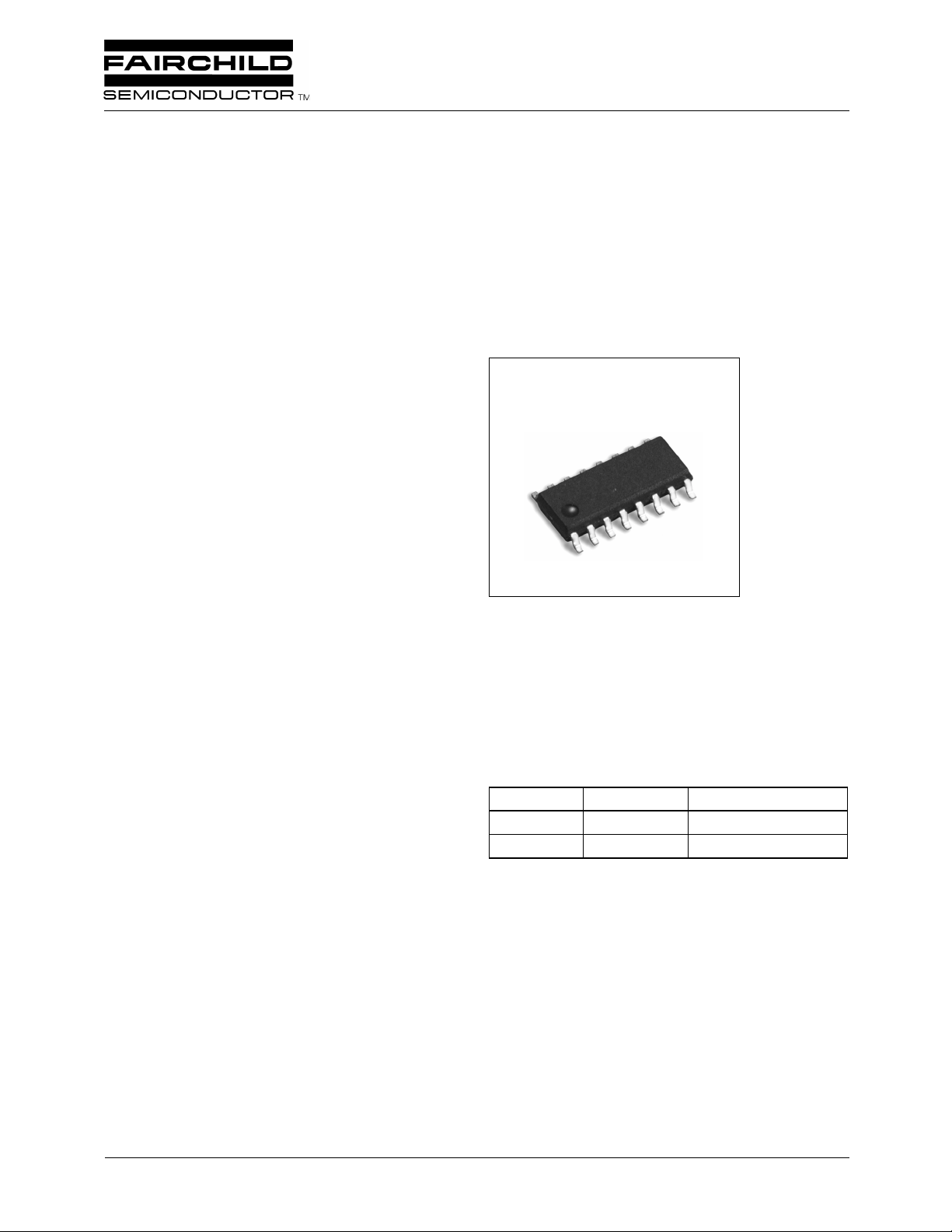
16-SOP-225
: 1A)
Typical Application
• Floppy disk drive
• Camera stepping motor
• General stepping motor
©2000 Fairchild Semiconductor International
Ordering Information
Device Package Operating Temp.
KA3100D 16-SOP-225 −20 ~ +75°C
KA3100DTF 16-SOP-225 −20 ~ +75°C
Rev. 1.0.2
May. 2000.
1
Page 2
KA3100D
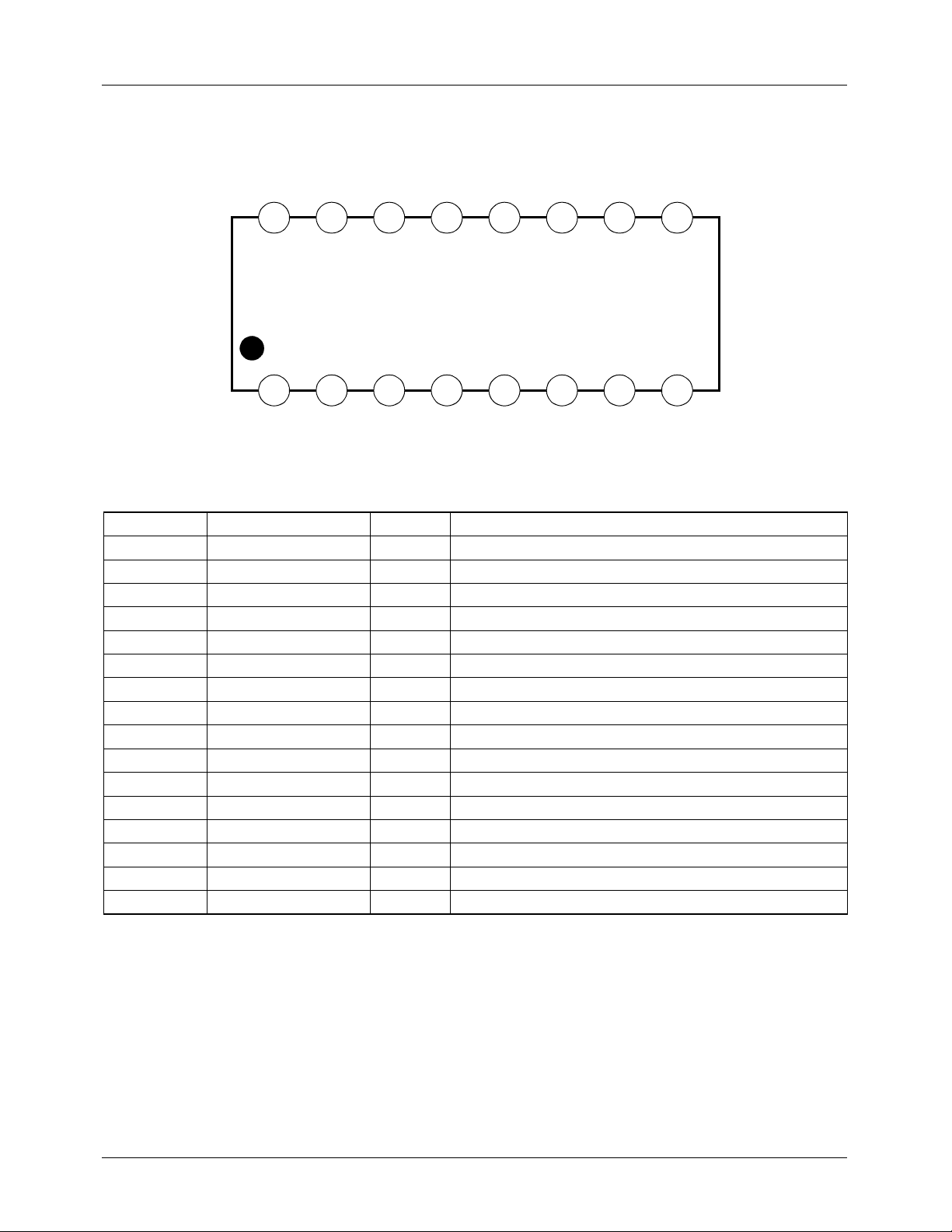
Pin Assignments
PGND
CE2
OUT3
VS2
OUT4
IN2
NC
NC
910111213141516
KA3100D
12345678
CC
V
CE1
OUT1
VS1
OUT2
IN1
SGND
PGND
Pin Definitions
Pin Number Pin Name I/O Pin Function Description
1V
CC
2 CE1 I Chip enable 1
3 OUT1 O Output 1
4 VS1 - Power supply 1
5 OUT2 O Output 2
6 IN1 I Input 1
7 SGND - Signal ground
8 PGND - Power ground
9 NC - No connection
10 NC - No connection
11 IN2 I Input 2
12 OUT4 O Output 4
13 VS2 - Power supply 2
14 OUT3 O Output 3
15 CE2 I Chip enable 2
16 PGND - Power ground
- Logic part supply voltage
2
Page 3
Internal Block Diagram
V
1
CC
IN1
6
CE1
2
SGND
7
Control
Part1
TSD &
BIAS
KA3100D
4
VS1
3
OUT1
5
OUT2
8
PGND
13
VS2
IN2
CE2
14
OUT3
11
Control
Part2
15
10 9
NC NC
12
OUT4
16
PGND
3
Page 4

KA3100D
Absolute Maximum Ratings (Ta = 25°C)
Parameter Symbol Value Unit
Supply voltage V
Power supply voltage V
Output voltage V
Input voltage V
Peak output current I
CC(MAX)
S(MAX)
OUT(MAX)
IN(MAX)
O(PEAK)
Continuous output current I
Power dissipation P
Junction temperture T
Storage temperature T
Operating temperature T
O
D
J
STG
A
9.0 V
9.0 V
VS + Vef V
7.0 V
1A
0.4 A
0.55 W
150 °C
−40 ~ 125 °C
−20 ~ 75 °C
Power Dissipation Curve
1.33
Power
Dissipation
: PD[W]
1.0
0.5
0
0 25 50 75 100 125
Ambient temperature, Ta [°C]
150 175
Power dissipation decreases at the rate of 13.6mV / °C when mounted on 30mm × 30mm × 1.5mm PCB (Phenolic resin mate-
rial) and used above Ta=25°C.
Recommended Operating Conditions (Ta = 25°C)
Parameter Symbol Min. Typ. Max Unit
Logic circuit supply voltage V
Power supply voltage V
CC
S
2.5 - 7.0 V
2.5 - 7.0 V
4
Page 5

Electrical Characteristics
(Ta=25°C, VCC=5V, VS1=3V, VS2=3V, unless specified otherwise)
Parameter Symbol Conditions Min. Typ. Max. Units
Supply current 1 I
Supply current 2 I
Saturation voltage 1 V
Saturation voltage 2 V
Input high level voltage V
Input low level voltage V
Input current I
Chip enable current I
Clamp diode leakge current I
Clamp diode voltage V
CC1
CC2
SAT1
SAT2
INH
INL
IN
CE
LEAK
EF
CE1, 2=0V, V
or 0V, Each CH.
CE1=3V, V
or 0V, Each CH.
CE1=3V, V
or 0V, I
CE1=3V, V
or 0V, I
VIN=3V, Each CH - 100 200 uA
CE=0V, Each CH - 100 200 uA
VCC=7V, VS=7V - - 30 uA
I
OUT
KA3100D
=3V
INL
=3V
INL
=3V
INL
=0.2A
OUT
=3V
INL
=0.4A
OUT
-1.8-V
- 0.1 10 uA
-1218mA
-0.20.3V
-0.40.6V
CC
- −0.3 - 0.7 V
=0.4A - - 1.7 V
V
Function Descriptions
IN1 & IN2 CE1 & CE2 OUT1 & OUT3 OUT2 & OUT4 Motor rotatio n
Low High High Low Forward
High High Low High Reverse
Low Low Off Off Stand-by
High Low Off Off Stand-by
Typical Performance Characteristics
v
out(sat)
vs io Characteri stic Graph
1.0
0.8
V
OUT(SAT)
[V]
0.6
0.4
0.2
0
0 100 200 300 400 500 600 700
I
[A]
O
5
Page 6

KA3100D
Test Circuits
V
CC
V
CC
IN1
CE1
SW1
104pF
1
6
2
Control
Part1
SW2
VS1
4
OUT1
3
OUT2
5
SW4
SW5
15Ω6Ω
SW3
SGND
IN2
CE2
PGND
7
TSD &
BIAS
11
Control
Part2
15
10 9
NC NC
8
VS2
13
OUT3
14
OUT4
12
PGND
16
SW6
6Ω
SW7
15Ω
6
Page 7

Typical Application Circuits
V
CC
V
CC
1
IN1
6
104
Control
Part1
KA3100D
VS1
4
OUT1
3
From controller
CE1
SGND
IN2
CE2
OUT2
2
7
TSD &
BIAS
11
Control
Part2
15
10 9
NC NC
5
PGND
8
Step
Motor
VS2
13
OUT3
14
OUT4
12
PGND
16
7
Page 8

KA3100D
DISCLAIMER
FAIRCHILD SEMICONDUCTOR RESERVES THE RIGHT TO MAKE CHANGES WITHOUT FURT HER NOTICE TO ANY
PRODUCTS HEREI N TO IMPROVE RELIABILITY, FUNCTIO N OR DESIGN. FAIRCH IL D DOES NOT ASSUME ANY
LIABILITY ARISING OUT OF THE APPLICATION OR USE OF ANY PRODUCT OR CIRCUIT DESCRIBED HEREIN; NEITHER
DOES IT CONVEY ANY LICENSE UNDER IT S PATENT RIGHTS, NOR THE RIGHTS OF OTHE RS.
LIFE SUPPORT POL I CY
FAIRCHILD’S PR ODUCTS ARE NOT AUTH ORIZED FOR USE AS C RITICAL COMPONENT S IN LIFE SUPPORT DE VICES
OR SYSTEMS WITHOUT THE EXPRESS WRITTEN APPROVAL OF THE PRESIDENT OF FAIRCHILD SEMICONDUCTOR
INTERNATIONAL. As used herein:
1. Life support devices or systems are devices or systems
which, (a) are intended for surgical implant into the body,
or (b) support or sustain life, and (c) whose failure to
perform when properly used in accordance with
2. A critical component in any component of a life support
device or sy stem whose fai lure to perform can be
reasonably expec ted to cause the failur e of the life support
device or system, or to affect its safety or effec t iv ene ss .
instructions for use provided in the labeling, can be
reasonably expected to result in a significant injury of the
user.
www.fairchildsemi.com
12/1/00 0.0m 001
2000 Fairchild Semiconductor International
Stock#DSxxxxxxxx
 Loading...