

Page 1
KA3524
SMPS Controller
www.fairchildsemi.com
Features
• Complete PWM power control circuit
• Operation beyond 100KHz
• 2% frequency stability with temperature
• Total quiescent current less than 10mA
• Single ended or push-pull outputs
• Current limit amplifier provides external component
protection
• On-chip protection against excessive junction temperature
and output curre nt
• 5V, 50mA linear regulator output available to user
Description
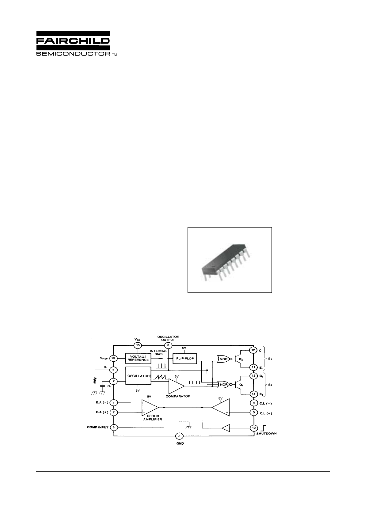
The KA3524 regul ating pulse width modulator contains
all of the control circuit necessary to implement switching
regulators of either polarity, transformer coupled DC to
DC converters, transforme r le ss pola r it y conv e rte r s and vol tage doublers, as well as other power control applications.
This device incl udes a 5V vol tag e regu lat or cap able of supplying up to 50mA to external circuit , a control amplifier, an oscillator, a pulse width modulator, a phase
splitting flip-flop, dual alternating output switch transistors,
and current limiting and shut-down circuit. Both the regulator output transistor and each output switch are internally
current limiting and, to limit junction temperature, aninternal thermal shutdown circuit is employed.
16-DIP
1
Internal Block Diagram
©2000 Fairchild Semiconductor International
Rev. 5.0
Page 2
KA3524
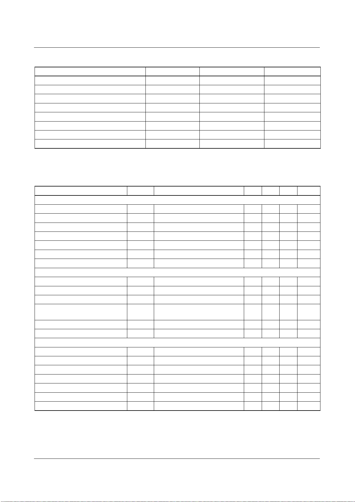
Absolute Maximum Ratings
Parameter Symbol Value Unit
Supply Voltage V
Reference Output Current I
Output Current (Each Output) I
Oscillator Charging Current (pin 6 or 7) I
CHG(OSC
Lead Temperature (Soldering, 10 sec) T
Power Dissipation (T
= 25°C) P
A
Operating Temperature T
Storage Temperature T
CC
REF
O
)5 mA
LEAD
D
POR
STG
40 V
50 mA
100 mA
300 °C
1000 mW
0 ~ +70 °C
-65 ~ + 150 °C
Electrical Characteristics
(VIN=20V, f=20KHz, TA = 0 to +70°C, unless otherwise specified)
Parameter Symbol Conditions Min. Typ. Max. Unit
REFERENCE SECTION
Reference Output Voltage V
Line Regulation ∆V
Load Regulation ∆V
REF
REFVCC
REFIREF
= 8V to 40V - 10 30 mV
= 0 mA to 20 mA - 20 50 mV
Ripple Rejection RR f = 120Hz, T
V
Short-Circuit Output Current I
Temperature Stability ST
SC
T
Long Term Stability ST T
= 0, TA = 25°C - 100 - mA
REF
= 25°C-20-mV/KHr
A
OSCILLATOR SECTION
Maximum Frequency f
(MAX)
Initial Accuracy ACCUR R
Frequency Change with Voltage ∆f/∆V
Frequency Change with
Temperature
Clock Amplitude (Pin 3) V
Clock Width (Pin 3) t
∆f/∆T Over operating temperature range - - 2 %
(CLK)TA
W(CLK)CT
CT = 0.001uF, RT = 2KΩ - 350 - KHz
and CT constant - 5 - %
T
CCVCC
= 8V to 40V, TA = 25°C--1%
= 25°C-3.5-V
= 0.01uF, TA = 25°C-0.5-µs
ERROR AMPLIFIER SECTION
Input Offset Voltage V
Input Bias Current I
Open Loop Voltage Gain G
Common-Mode Input Voltage V
BIAS
VO
CM
Common-Mode Rejection Ratio CMRR T
Small Signal Bandwidth BW
Output Voltage Swing V
O(ERR)TA
VCM = 2.5V - 2 10 mV
IO
VCM = 2.5V - 2 10 µA
TA = 25°C1.8-3.4V
= 25°C-70-dB
A
GV = 0dB, TA= 25°C-3-MHz
SS
= 25°C0.5-3.8V
-4.65.05.4V
= 25°C-66-dB
A
--0.31%
-6080-dB
2
Page 3
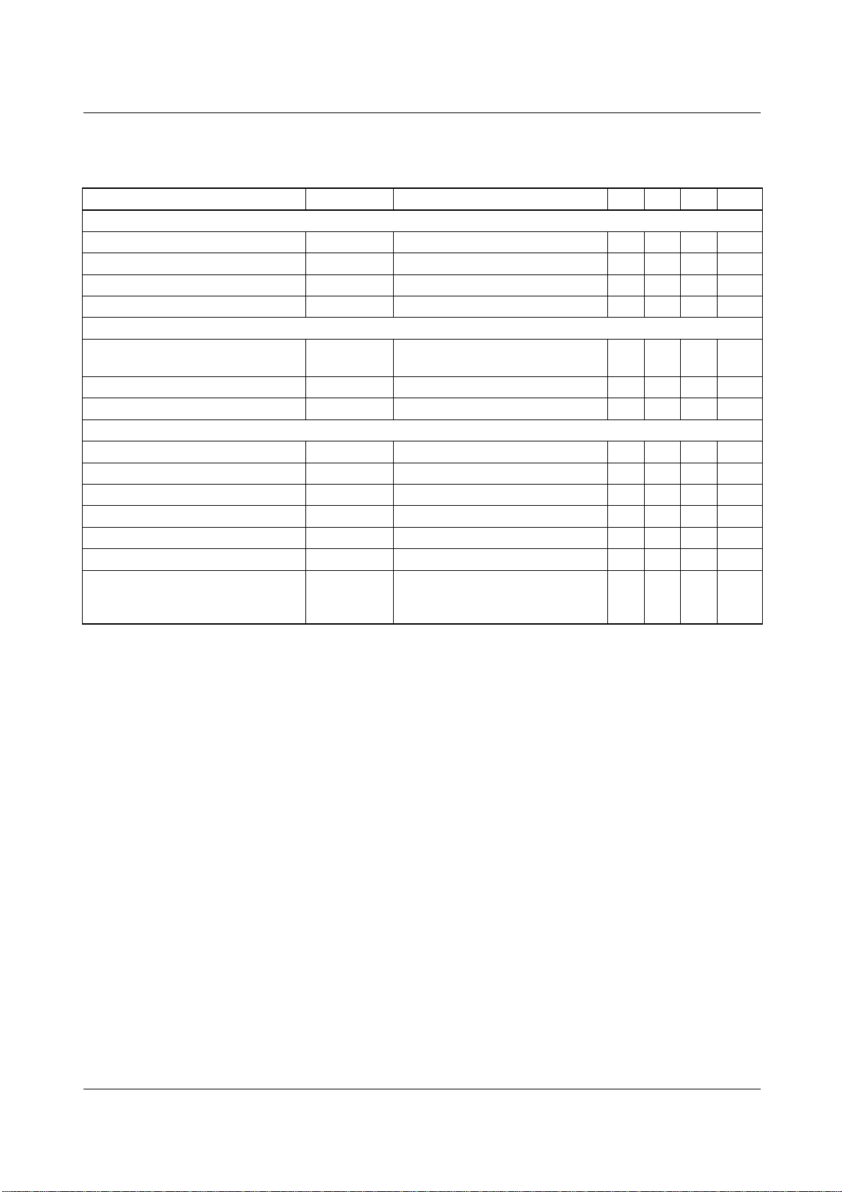
Electrical Characteristics
(VIN=20V, f=20KHz, TA=0°C to +70°C, unless otherwise specified)
Parameter Symbol Conditions Min. Typ. Max. Unit
COMPARATOR SECTION
Maximum Duty Cycle D
(MAX)
Input Threshold (Pin 9) V
Input Threshold (Pin 9) V
Input Bias Current I
BIAS
CURRENT LIMITING SECTION
Sense Voltage V
Temperature Coefficient of Vsense ∆V
SENSE
SENSE
Common-Mode Voltage V
OUTPUT SECTION (EACHOUTPUT)
Collector-Emitter Voltage V
Collector Leakage Current I
Saturation Voltage V
CE(SAT)
Emitter Output Voltage V
Rise Time (10 to 90) t
Fall Time (90 to 10) t
Supply Current I
TH1
TH2
CM
CEO
LKG
E
R
F
CC
% Each output on 45 - - %
Zero duty cycle - 1 - V
Maximum duty cycle - 3.5 - V
V2 - V
1
V
= 2V, TA = 25°C
9
/∆T- -0.2-mV/°C
VCE = 40V - 0.1 50 µA
IC = 50mA - 1 2 V
VC = 20V 17 18 - V
RC = 2KΩ, TA = 25°C-0.2-µs
RC = 2KΩ, TA = 25°C-0.1-µs
VCC =40V, PINS 1,4,7,8,11
and 14 are grounded, V
All other inputs and Outputs open
≥50mV
KA3524
--1-µA
180 200 220 mV
-0.7-1V
-40--V
2
=2V
-510mA
3
Page 4
KA3524
Application Information
Voltage Reference
An internal series regulator provides a nominal 5 volt output which is used both to generate a reference voltage and is
the regulated source for all the internal timing and controlling circuitry . This regulator may be bypassed for operation
from a fixed 5 volt supply by connecting pins 15 and 16 together to the input voltage. In this configuration, the maximum
input voltage is 6.0 volts.
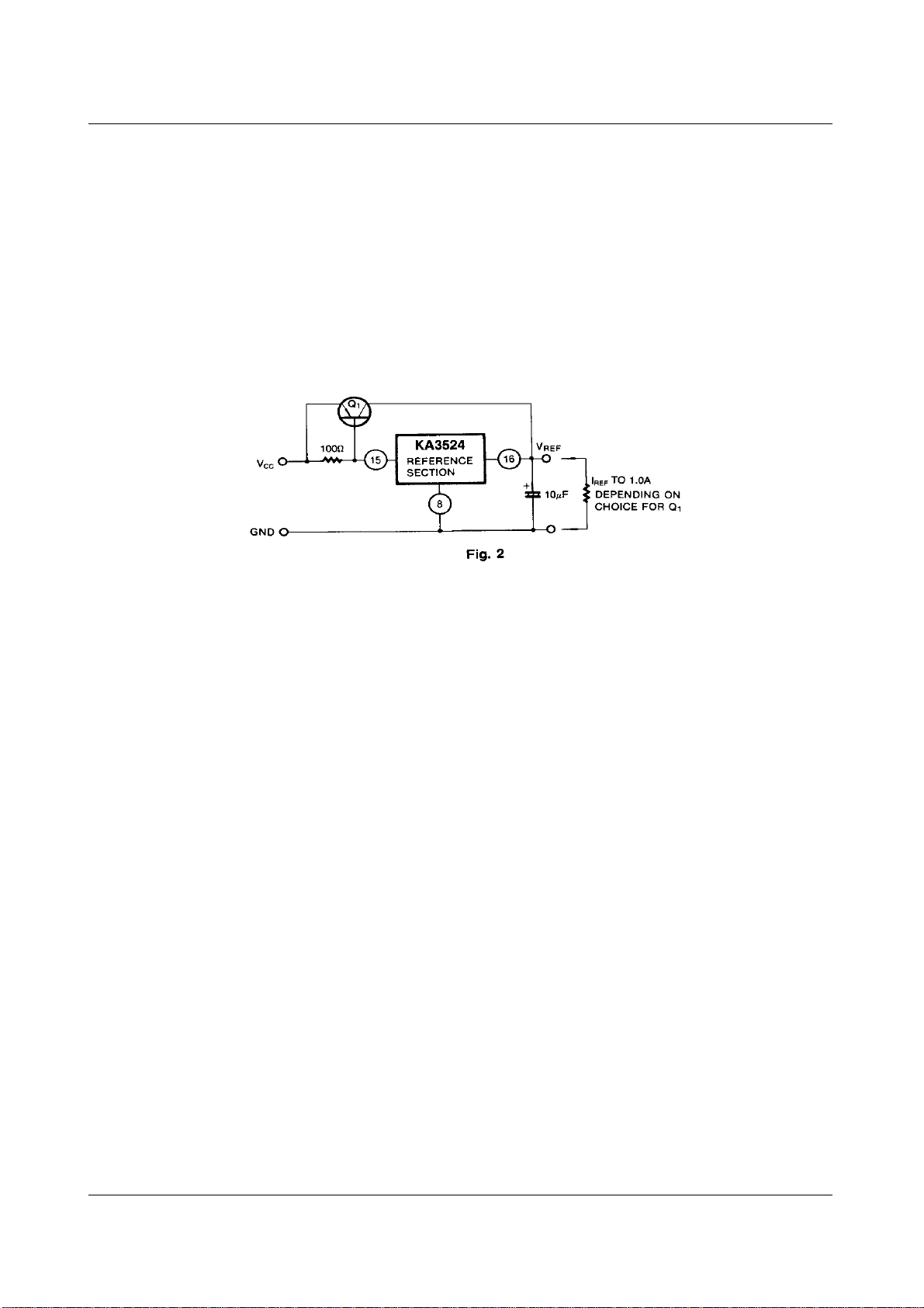
This reference regulator may be used as a 5 volt source for other circuitry. It will provide up to 50mA of current itself
and can easily be expanded to higher current with an external PNP as shown in Figure 2.
Expanded Reference Current Capability
Oscillator
The oscillator in the KA3524 uses an external resistor (RT) to establish a constant charging current into an external capacitor
(C
), While this uses more current than a series connected PC, it provides a linear ramp voltage on the capacitor which is also
T
used as a reference for the comparator. The charging current is equal to 3.6V/R
approximately 30uA to 2mA, i.e., 1.8K< R
<100K. The range of values for CT also has limits as the discharge time of C
T
and should be kept within the range of
T
t
determine s the pulse widt h of the oscillator outpu t pulse. This pulse is used (among other t hings) as a bla nking pulse to both
outputs to insure that there is no possibility of having both outputs on simultaneously during transitions. This output dead time
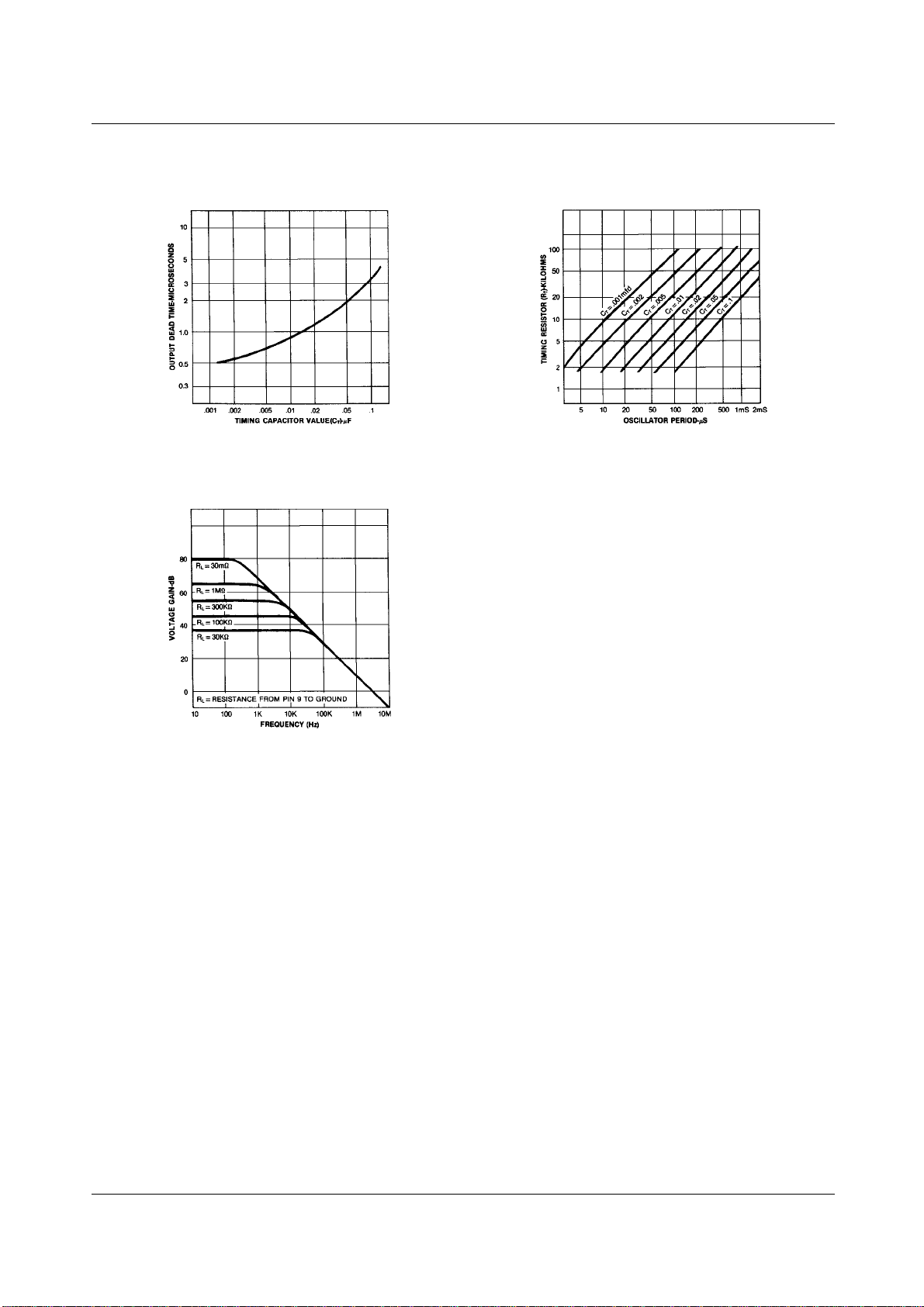
relationship is shown in Figures. A pulse width below approximately 0.5 microseconds may allow false triggering of one output by removing he blanking pulse prior to the flip-flops reaching a stable state. If small values of C
must be used, the pulse
T
width may still be expanded by adding a shunt capacitance (= 100pF) to ground at the oscillator output. (Note: Although the
oscillator output is a convenient oscilloscope sync input, the cable and input capacitance may increase the blanking pulse
width slightly.) Obviously, the upper limit of the pulse width is determined by the maximum duty cycle acceptable. Practical
values of C
onds when R
fall between 0.01 and0.1 micro farad. The oscillator period is approximately t = RTCT where t is in microsec-
T
ohms and CT = micro farads. The selection of RT and CT can be made for a wide range of operating frequen-
T
cies by using Fig. 7. Note that for sense regulator applications, the two outputs can be connected in parallel for an effective 090% duty cycle and the frequen cy of the os cillat or is the fr equenc y of the ou tput. Fo r push-p ull appl ications, the outp uts are
separated and the flip-flop divides the frequency such that each output duty cycle is 0-45% and the overall frequency is onehalf that of the oscillator.
External Synchronization
If It is desired to synchronize the KA3524 to an external clock, a pulse of +3 volts may be applied to the oscillator output
terminal with R
ground at this point is approximately 2K ohms. If two or more KA3524s must be synchronized together, one must be designated as the master with its R
10% longer period than the master with the added requirement that C
on all units together will insure that the master output pulse-which occurs first and has a wider pulse width - will reset the
slave units.
set slightly greater than the clock period. The same considerations of pulse width apply . The impedance to
TCT
set for the correct period. The slaves should each have an RTCT set for an approximately
TCT
(slave) = one-half CT (master). Then connecting Pin 3
T
4
Page 5
KA3524
Error Amplifier
This circuit is a simple differential-input, transconductance amplifier. The output is the compensation terminal pin 9, which is
a high impedance node (R
8I
G
= gmRL = = 0.002 R
V
LRL
---------------
2K
T
=5MΩ). The gain is
L:
L
and can easily be reduced from a nominal of 10,000 by an external shunt resistance from pin 9 to ground, as shown in Figure
8,In addition to DC gain control, the compensation terminal is also the place for AC phase compensation. The frequency
response curves of Figure 5 show the uncompensated amplifier with a single pole at approximately 200Hz and a unity gain
cross-over frequency at 5MHz.typically, most output filter designs will introduce one or more addition poles at a significantly
higher power frequency. Therefore, the best stabilizing network is a series R-C combination between pin 9 and ground which
introduces a zero to can cel one of the ou tput filte r poles. A good starting point is 50KΩ plus 0.001 micro farad. O ne final poin t
on the compensation terminal is that this is also a convenient place to insert any programming signal which is to override the
error amplifier. Internal shutdown and current limit circuits are connected here, but any other circuit which can sink 200uA
can pull this point to ground, thus shutting off both outputs. While feedback is normally applied around the entire regulator, the
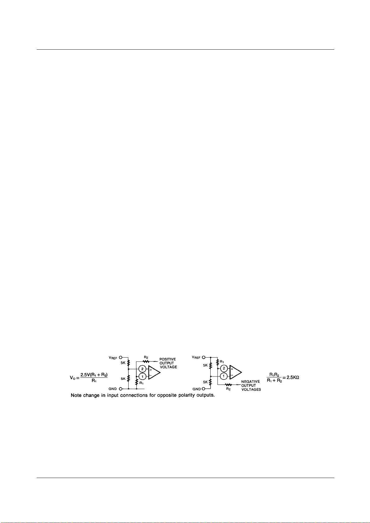
error amplifier can be used with conventional operational amplifier feedback and is stable in either the inverting or noninverting mode. Regardless of the connections, however, input common-mode limits must be observed or output sign inversions may happen. Fo r co nven tion al re gula tor a ppli catio ns, t he 5 v olt re fere nce vo lta ge mu st be d ivid ed do wn as sh own in Figure 3. The error amplifier may also be used in fixed duty cycle applications by using the unity gain configuration shown in the
open loop test circuit.
Current Limiting
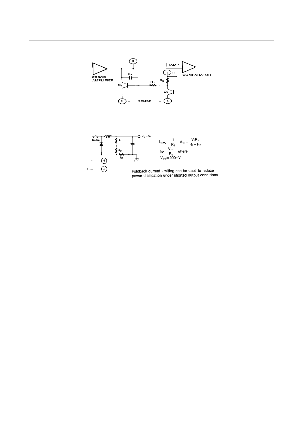
The current limiting circuitry of the KA3524 is shown in Figure 4.
By matching the base-emitter voltages of Q1 and Q2, and assuming negligible voltage drop across R
1 :
Threshold = VBE(Q1) + I 1R
= l
1R 2
= 200mV
2
- V
BE
(Q2)
Although this circuit provides a relatively small threshold with a negligible temperature coefficient, there are some limitations
to its use, the most important of which is the ±1 volt common mode range which requires sensing in the ground line. Another
factor to consider is that the frequency compensation provided by R
and Q1 provides a roll-off pole at approximately
1C1
300Hz.Since the gain of this circuit is relatively low, there is a transition region as the current limit amplifier takes over pulse
width control from the error amplifier. For testin g purposes, the th reshold is defined as th e input v oltage to get 25% d uty cy cle
with the error amplifier signaling maximum duty cycle. In addition to constant current limiting, pins 4 and 5 may also be used
in transformer-coupled circuits to sense primary current and shorten an output pulse, should transformer saturation occur.
Another application is to ground pin 5 and use pin 4 as an additional shutdown terminal: i.e., the output will be off with pin 4
open and on when it is grounded. Finally, fold back current limiting can be provided with the network of Figure 5. This circuit can reduce the short circuit current (l
)to approximately one third the maximum available output current (I
SC
Figure 3. Error Amplifier Biasing Circuits
MAX
).
5
Page 6
KA3524
Figure 4. Current Limiting Circuit Of The Ka3524
Figure 5. Foldback Current Limiting
6
Page 7
Typical Performance Characteristics
KA3524
Figure 6. Output Stage Dead Time As A Function Figure 7. Oscillator Period As A Function Of R
Of The Timing Capacitor Value
Figure 8. Amplifies Open-loop Gain As A Function Of
Freguency And Loading On Pin 9
And Ct
t
7
Page 8
KA3524
Typical Applications
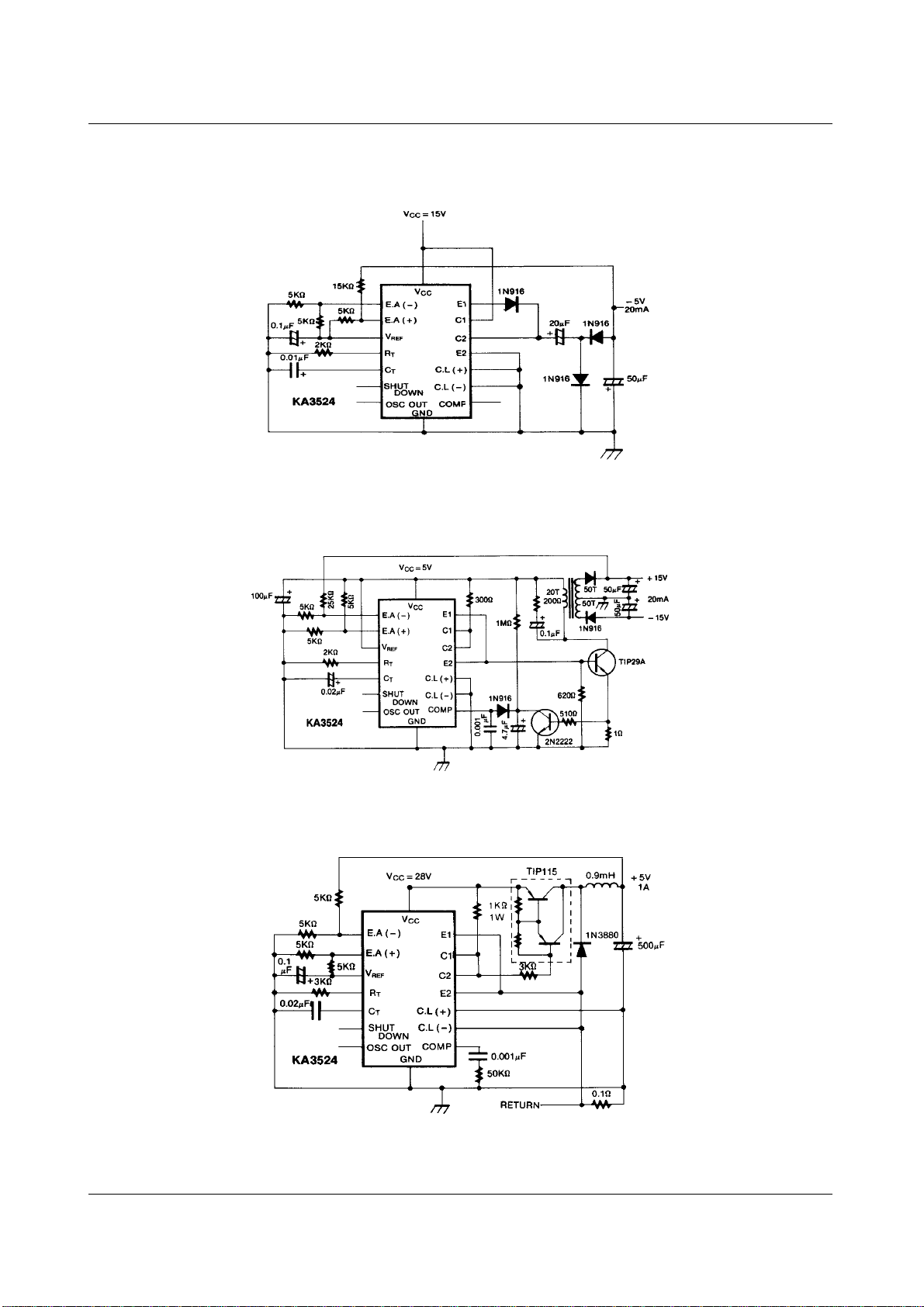
Figure 9. Capacitor-diode Output Circuit
Figure 10. Flyback Converter Cir cuit
Figure 11. Single-ended Lc Circuit
8
Page 9
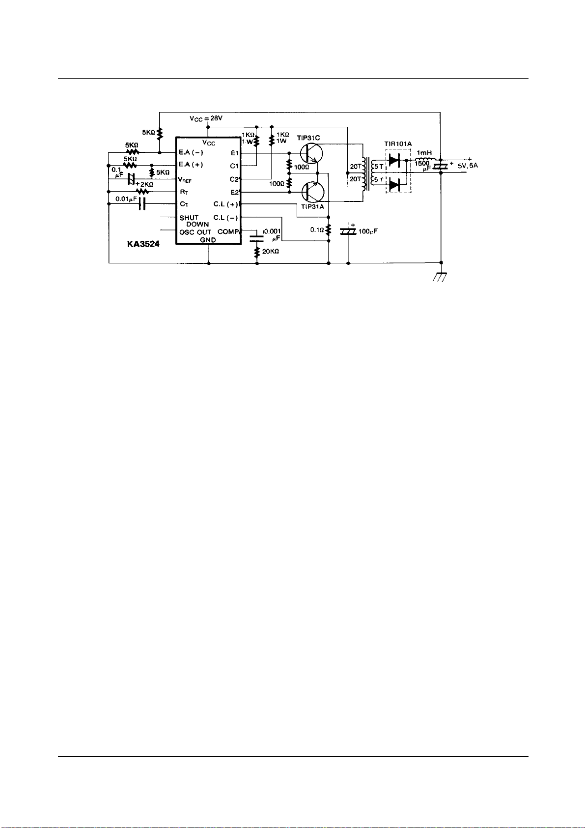
Figure 12. Push-pull Transformer-coupled Circuit
KA3524
9
Page 10
KA3524
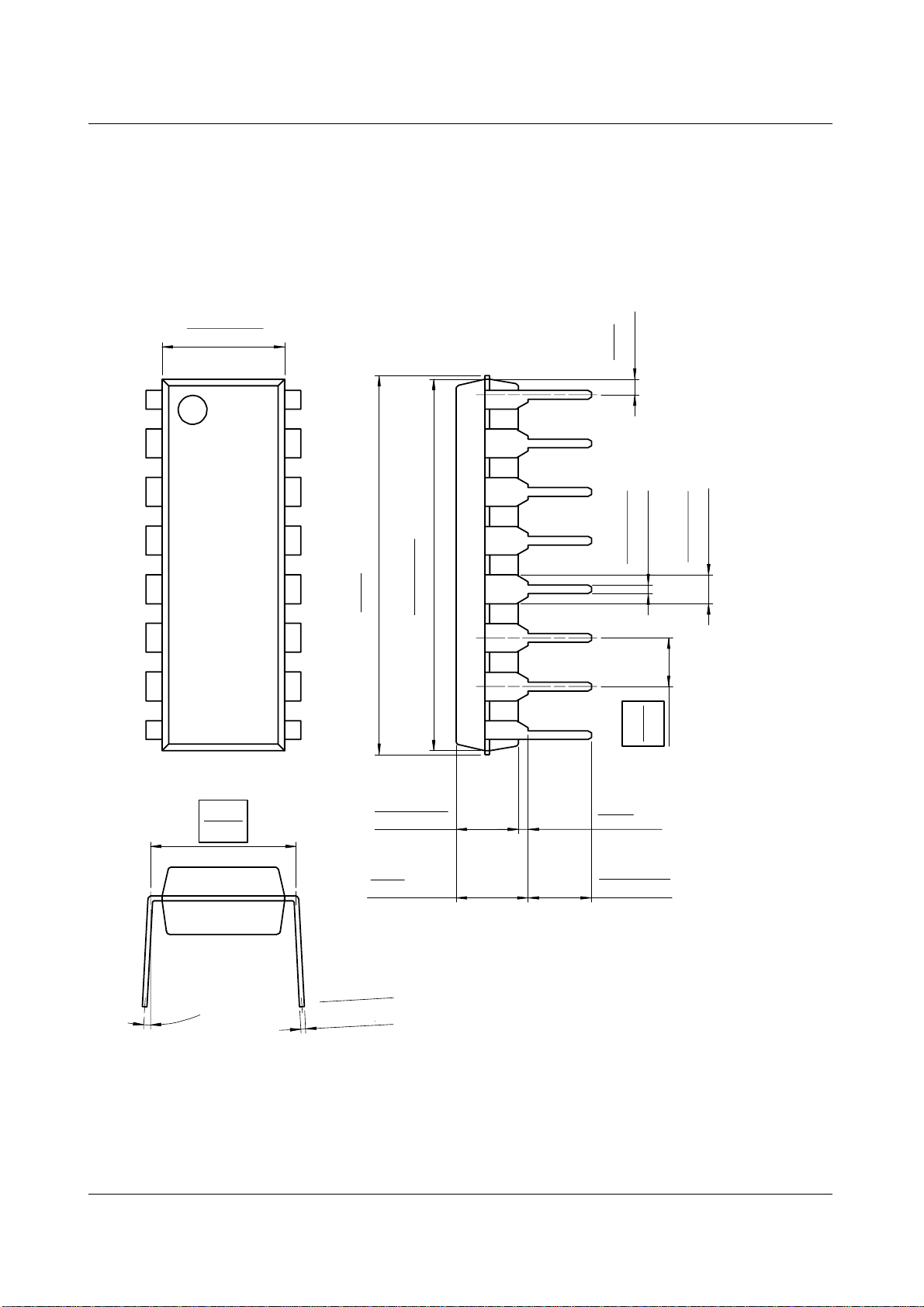
Mechanical Dimensions
Package
6.40 ±0.20
0.252 ±0.008
16-DIP
Dimensions in millimeters
0.81
0.032
()
#1
#8
7.62
0.300
#16
#9
MAX
19.80
0.780
3.25 ±0.20
0.128 ±0.008
19.40 ±0.20
0.764 ±0.008
0.38
0.014
±0.10
0.46
2.54
MIN
0.018 ±0.004
0.100
1.50 ±0.10
0.059 ±0.004
10
0~15°
0.25
0.010
5.08
0.200
+0.10
–0.05
+0.004
–0.002
MAX
3.30 ±0.30
0.130 ±0.012
Page 11

Ordering Information
Product Number Package Operating Temperature
KA3524 16-DIP 0 ~ 70°C
KA3524
11
Page 12

KA3524
DISCLAIMER
FAIRCHILD SEMICONDUCTOR RESERVES THE RIGHT TO MAKE CHANGES WITHOUT FURT HER NOTICE TO ANY
PRODUCTS HEREI N TO IMPROVE RELIABILITY, FUNCTIO N OR DESIGN. FAIRCH IL D DOES NOT ASSUME ANY
LIABILITY ARISING OUT OF THE APPLICATION OR USE OF ANY PRODUCT OR CIRCUIT DESCRIBED HEREIN; NEITHER
DOES IT CONVEY ANY LICENSE UNDER IT S PATENT RIGHTS, NOR THE RIGHTS OF OTHE RS.
LIFE SUPPORT POL I CY
FAIRCHILD’S PR ODUCTS ARE NOT AUTH ORIZED FOR USE AS C RITICAL COMPONENT S IN LIFE SUPPORT DE VICES
OR SYSTEMS WITHOUT THE EXPRESS WRITTEN APPROVAL OF THE PRESIDENT OF FAIRCHILD SEMICONDUCTOR
INTERNATIONAL. As used herein:
1. Life support devices or systems are devices or systems
which, (a) are intended for surgical implant into the body,
or (b) support or sustain life, and (c) whose failure to
perform when properly used in accordance with
2. A critical component in any component of a life support
device or sy stem whose fai lure to perform can be
reasonably expec ted to cause the failur e of the life support
device or system, or to affect its safety or effec t iv ene ss .
instructions for use provided in the labeling, can be
reasonably expected to result in a significant injury of the
user.
www.fairchildsemi.com
9/25/00 0.0m 001
2000 Fairchild Semiconductor International
Stock#DSxxxxxxxx
 Loading...