

Page 1
KA3501
PC SMPS Super visory IC
www.fairchildsemi.com
Features
• Complete House Keeping Circuit
• Few External Components
• Positive Voltage Protection
• Negative Voltage Protection
• High Current Drive Output for SCR
• Precision Voltage Reference for 5V/12V Outputs
• Power Good Signal Generat or with Hyster e sis
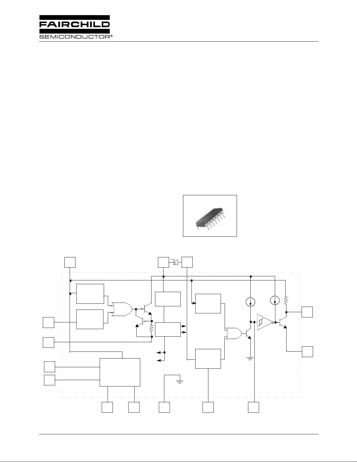
Internal Block Diagram
4
V
CC
1(+5V)
V
CC
Description
The KA3501 is complete housekeeping circuits for use in the
secondary side of SMPS(Switched Mode Power Supply).
This IC(Integrated Circuit) contains a precision voltage
reference, pr ot ection circuits and a power go od signal
generator. It also has a high current drive output for use in
conjunction with an external "crowbar" SCR. The reference
voltage is trimmed to ±2% for correct output voltages(+5V/
+12V) and power good signal generator is to monitor the
voltage level of power good supply for safe operation in a
microprocessor circuit. Using the KA3501 requires few
external components to accomplish a complete
housekeeping circuit for SMPS(Switched Mode Power
Supply). The KA3501 is available in an 14-pin DIP.
14-DIP
1
7
8
Vin1
Positive
Voltage
Protection
Vin2
5
GATE
6
Feedback
14
2
Vref
©2002 Fairchild Semiconductor Corporation
Negative
Voltage
Protection
V
CC
2(+12V)
+2.5V
REFERENCE
VOLTAGE
3
1
Vcont
START UP
INTERNAL
BIAS
13
GND
+5V
Detecting
COMP
V
CC
Detecting
COMP
9
Td
lchg
10
11
PG
12
Ve
Timing
Rev. 1.0.2
Page 2
KA3501
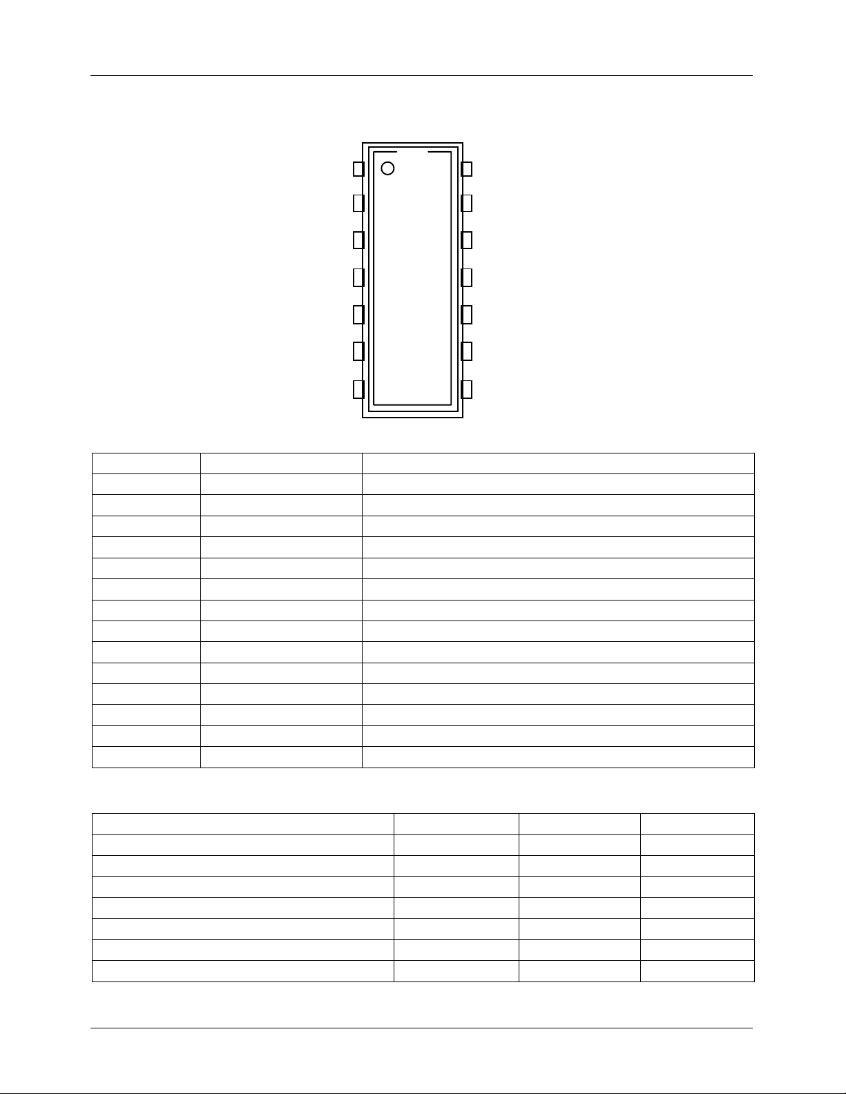
Pin Assignments
#14
Feedback
GND
Ve
Vcont
Vref
Vcc2
#1
K
A
Vcc1
3
PG
5
Vin2
0
Tim ing
1
Gate
Vcc
#7 #8
Pin Number Pin Name Pin Function Description
1 Vcont Reference Voltage Control
2 Vref Precision Reference Voltage
3 Vcc2 +12V Output Voltage
4 Vcc1 +5V Output Voltage
5 Vin2 UVP Input (Negative)
6 Gate Gate Drive Input for SCR
7 Vcc Supply Voltage
8 Vin1 PG Input
9 Td Reference Voltage Delay for PG
10 Timing PG Delay
11 PG PG Output
12 Ve PG Ground (Open Emitter)
13 GND Ground
14 Feedback Feedback for Precision Reference
Td
Vin1
Absolute Maximum Rating ( Ta = 25°°°°C)
Parameter Symbol Value Unit
Supply Minimum Voltage Vcc(min) 5 V
Supply Maximum Voltage Vcc(max) 35 V
UV Input Voltage Vuv 24 V
Minimum Gate Drive Current I
Operating Cathode Current I
Power Dissipation Pd 1 W
Operating Temperature Range Topr 0 to 70 °C
2
DR
K
-25 V
1 to 30 A
Page 3
KA3501
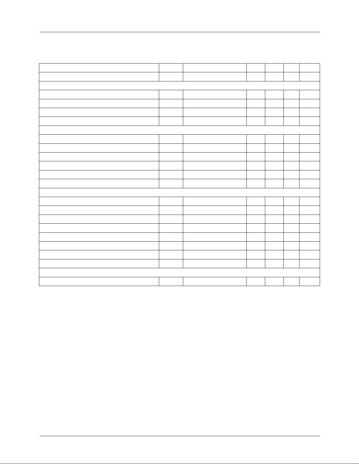
Electrical Characteristic
(Refer to the test circuit , Vcc=20V, Ta=25°C, unless otherwise stated)
Parameter Symbol Conditions Min. Typ. Max. Unit
Temperature Stability for V
REF
∆V
REF
PROTECTION SECTION
Positive Protection Voltage V
Negative Protection Voltage V
Negative Input Resistor R
Gate Drive Current I
POSI
NEGA
NEGA
DR
Vcc1 = 5V -1.5 -2.5 -3.5 V
Pin 4 to Pin 5 8.5 10 11.5 kΩ
V
GATE
REFERENCE SECTION
Reference Input Voltage V
Current Stability ∆V
REFIK
REFIK
= 10mA 2.44 2.50 2.56 V
=1mA to 10mA - 5 20 mV
Absolute Precision of Internal Three Resistors Rint - - - ±20 %
Relative Deviation of Three Resistors Rrate - - ±0.5 ±3%
Temperature Stability (Note1) ∆V
Ta = 0 to 70 °C - 13 17 mV
REF
Gain Bandwidth (Note1) GBW GV = 1 - 1 - MHz
POWER GOOD SECTION
Detecting Input Voltage V
Detecting PG Voltage V
IN1
DET
Hysteresis Voltage 1 HY1 - 10 20 40 mV
Hysteresis Voltage 2 HY2 - 200 250 - mV
Charging Current for PG Delay I
PG Output Resistor R
PG Output Saturation Voltage V
PG Output Leakage Current I
CHG
PG
SATISINK
O(LKG)
TOTAL STANDBY CURRENT
Supply Current Icc V
CC
--17-mV
- 5.7 6.0 6.4 V
= 0.7 V -25 -50 - V
- 1.23 1.28 1.33 V
- 4.1 4.3 4.5 V
--8-14-20uA
- 7.7 9.0 10.3 kΩ
= 6mA - 0.2 0.4 V
- - 0.01 1 uA
= 20V , V
= 5V - 3 5 mA
CC1
Note:
1.These parameters, although guaranteed, are not 100% tested in production
3
Page 4
KA3501
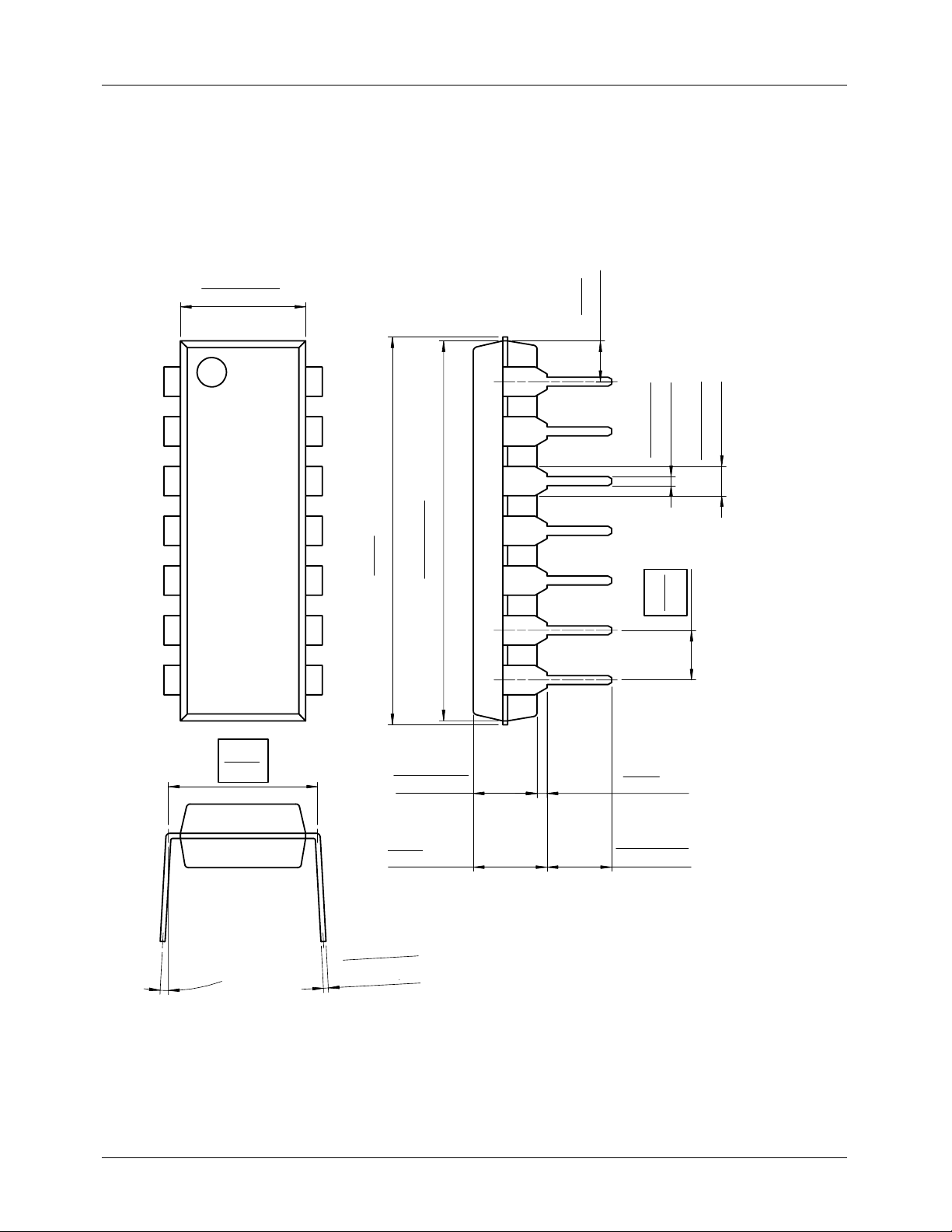
Mechanical Dimensions
Package
6.40
±0.20
±0.008
0.252
14-DIP
Dimensions in millimeters
2.08
0.082
()
#1
#7
7.62
0.300
#14
#8
MAX
19.80
0.780
±0.20
19.40
3.25
0.128
±0.008
0.764
±0.20
±0.008
0.20
0.008
±0.10
0.46
2.54
MIN
±0.004
0.018
0.100
±0.10
1.50
±0.004
0.059
3.30
0.130
±0.30
±0.012
0~15°
0.25
0.010
5.08
0.200
+0.10
–0.05
+0.004
–0.002
MAX
4
Page 5

Ordering Information
Product Number Package Operating Temperature
KA3501 14-DIP 0°C ~ +70°C
KA3501
5
Page 6

KA3501
DISCLAIMER
FAIRCHILD SEMICONDUCTOR RESERVES THE RIGHT TO MAKE CHANGES WITHOUT FURT HER NOTICE TO ANY
PRODUCTS HEREI N TO IMPROVE RELIABILITY, FUNCTIO N OR DESIGN. FAIRCH IL D DOES NOT ASSUME ANY
LIABILITY ARISING OUT OF THE APPLICATION OR USE OF ANY PRODUCT OR CIRCUIT DESCRIBED HEREIN; NEITHER
DOES IT CONVEY ANY LICENSE UNDER IT S PATENT RIGHTS, NOR THE RIGHTS OF OTHE RS.
LIFE SUPPORT POL I CY
FAIRCHILD’S PR ODUCTS ARE NOT AUTH ORIZED FOR USE AS C RITICAL COMPONENT S IN LIFE SUPPORT DE VICES
OR SYSTEMS WITHOUT THE EXPRESS WRITTEN APPROVAL OF THE PRESIDENT OF FAIRCHILD SEMICONDUCTOR
CORPORATION. As used herein :
1. Life support devices or systems are devices or systems
which, (a) are intended for surgical implant into the body,
or (b) support or sustain life, and (c) whose failure to
perform when properly used in accordance with
2. A critical component in any component of a life support
device or sy stem whose fai lure to perform can be
reasonably expec ted to cause the failur e of the life support
device or system, or to affect its safety or effec t iv ene ss .
instructions for use provided in the labeling, can be
reasonably expected to result in a significant injury of the
user.
www.fairchildsemi.com
10/9/02 0.0m 001
2002 Fairchild Semiconductor Corporation
Stock#DSxxxxxxxx
 Loading...