

Page 1
KA3082
Bi-Directional DC Motor Driver
www.fairchildsemi.com
Features
• Built-in Brake Function for Stable Brake Characteristics.
• Built-in Element to Absorb a Surge Current Derived From
Changing Motor Direction and Braking Motor Drive.
• Motor Speed Control by an External Voltage.
• Stable Motor Direction Change.
• Interfaces With CMOS Devices.
• Built-in the Thermal Shut Down Circuit (165°C).
• Low Standby Current. (6.5mA)
Description
The KA3082 is a monolithic integrated circuit designed for
driving bi-directional DC motor with braking and speed
control, and it is suitable for the loading motor driver of
VCR, CDP, and TOY systems. The speed control can be
achieved by adjusting the external voltage of the speed
control pin. It has two pins of logic inputs for control ling the
forward/ reverse and braking.
10-SIP
Target Appli cations
• Video Cassette Recorder (VCR) Loading Motor
• Low Current DC Motor Such as Audio or Video
Equipment.
• General DC Motor
©2002 Fairchild Semiconductor Corporation
Ordering Information
Device Package Operating Temp.
KA3082B 10-SIP -25°C ~ +75°C
Rev. 1.0.2
Page 2
KA3082
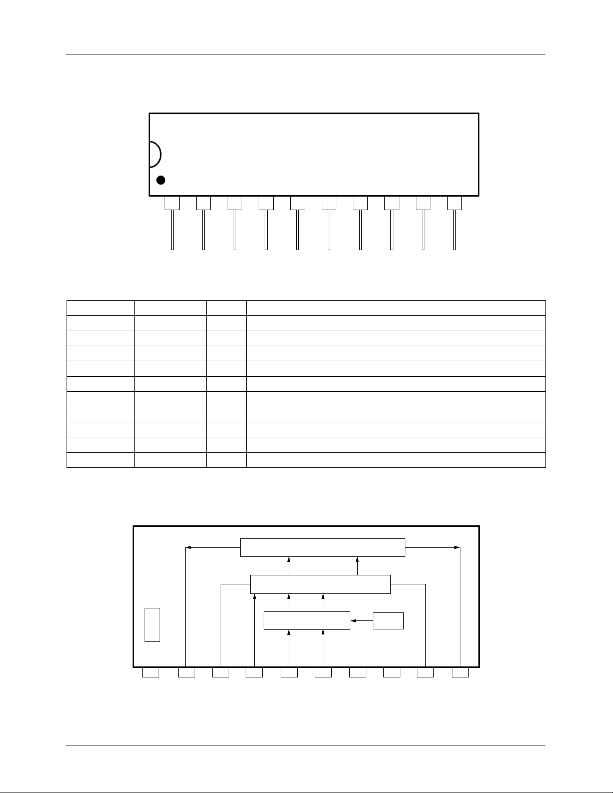
Pin Assignments
KA3082
GND V
12345678910
O1
V
V
Z1
CTLVIN1
V
IN2
SV
CC
PV
CCVZ2
Pin Definitions
Pin Number Pin Name I/O Pin Function Description
1 GND - Ground
2V
3V
4V
5V
6V
7SV
8PV
9V
10 V
O1
Z1
CTL
IN1
IN2
CC
CC
Z2
O2
O Output 1
- Phase Compensation
I Motor Speed Control
I Input 1
I Input 2
- Supply Voltage (Signal)
- Supply Voltage (Power)
- Phase Compensation
O Output 2
V
O2
Internal Block Diagram
BIAS
1234
GND
2
V
O1
DRIVER OUT
PRE DRIVER
LOGIC SWITCH
5
V
Z1
V
CTL
V
IN1
678910
V
IN2
SV
CC
TSD
PV
CC
Z2
V
O2
V
Page 3
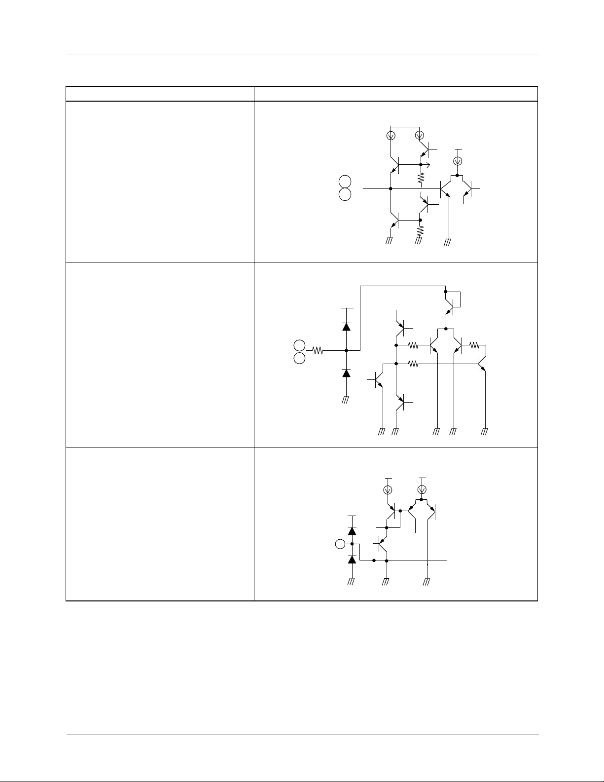
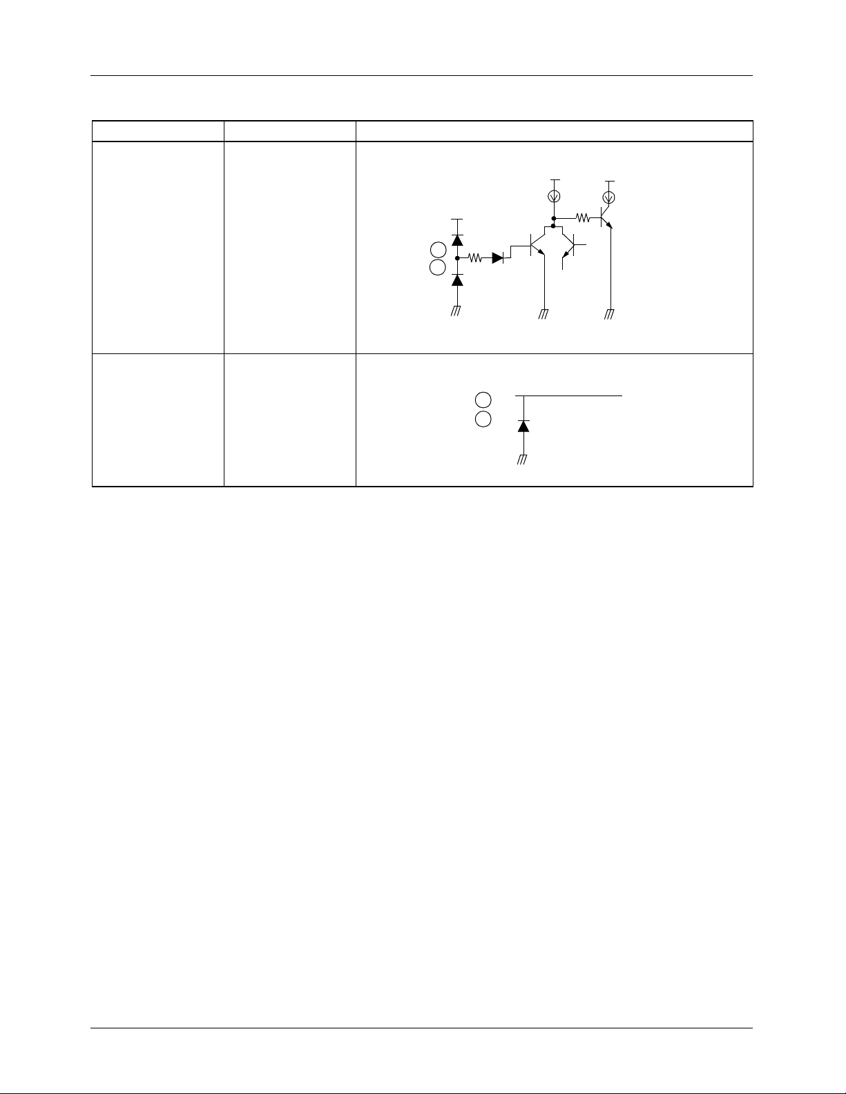
Equivalent Circuits
Description Pin No. Internal Circuit
KA3082
Vcc
Vcc
Output 2, 10
Phase
Compensation
3, 9
2
10
V
CC
50Ω
3
9
Speed Control 4
Vcc
VCC
4
Vcc
3
Page 4
KA3082
(Continued)
Equivalent Circuit
Description Pin No. Internal Circuit
Input 5, 6
SV
CC
PV
CC
Vcc
VCC
5
6
V
CC
7
8
7
8
Vcc
4
Page 5

Absolute Maximum Ratings (Ta=25°°°°C)
Parameter Symbol Value Unit Remark
Supply Voltage V
Maxium Output Current I
Power Dissipation P
Operating Temperature T
Storage Temperature T
Note:
1. Duty 1 / 100, pulse wid t h 50 0µs
2. 1) When mounted on glass epoxy PCB (76.2 × 114 × 1.57mm)
2) Power dissipation reduces 9.6mV / °C for using above Ta=25°C.
3)
Do not exceed Pd and SOA(Safe Operating Area).
CCmax
Omax
d
OPR
STG
18 V -
note1
1.6
1.2
note2
A-
W-
-25 ~ +75 °C-
-55 ~ +125 °C-
Power Dissipation Curve
Pd (mW)
KA3082
1, 200
SOA
0
0 25 50 75 100 125
150
Ambient temperature, Ta [°C]
15
Recommened Operating Conditions (Ta=25°°°°C)
Parameter Symbol Operating voltage range Unit
Operating Supply Voltage SV
Note:
Caution 1) PV
Caution 2) When PVCC is above 16V, the V
CC
≤ SV
CC
CTL
CC,PVCC
must be opened or 8.5 ≤ V
7 ~ 18 V
≤ PV
CTL
CC
5
Page 6

KA3082
Electrical Characteristics (Ta=25°°°°C, VCC=SVCC=PVCC=12V)
Parameter Symbol Conditions Min. Typ. Max. Unit
Quiescent Current I
Min. Input-on Current 1 I
Min. Input-on Current 2 I
Input Threshold Voltage 1 V
Input Threshold Voltage 2 V
Output Leakage Current 1 I
Output Leakage Current 2 I
Zener Current 1 I
Zener Current 2 I
Output Voltage 1 V
Output Voltage 2 V
Saturation Voltage 1 (Upper) V
Saturation Voltage 2 (Upper) V
Saturation Voltage 1 (Lower) V
Saturation Voltage 2 (Lower) V
CC2
IN1
IN2
ITH1
ITH2
OL1
OL2
Z1
Z2
O1
O2
SAT1IO
SAT2
SAT3
SAT4
Pin5 & 6: GND, RL=∞ 46.59.5mA
RL=∞, pin5=I
RL=∞, pin5=L, pin6=I
, pin6=L - 10 30 µA
IN1
IN
-1030µA
RL=∞, pin5=VIN, pin6=L 1.0 1.3 1.6 V
RL=∞, pin5=L, pin6=V
IN
1.0 1.3 1.6 V
RL=∞, pin5 & 6=GND - 0.01 1 mA
RL=∞, pin5 & 6=GND - 0.01 1 mA
RL=∞, pin5=H, pin6=L - 0.85 1.5 mA
RL=∞, pin5=L, pin6=H - 0.85 1.5 mA
RL=60Ω, pin5=H, pin6=L 6.6 7.2 7.6 V
RL=60Ω, pin5=L, pin6=H 6.6 7.2 7.6 V
=300mA - 1.9 2.3 V
IO=500mA - 1.9 2.3 V
IO=300mA - 0.25 0.5 V
IO=500mA - 0.4 0.65 V
6
Page 7

Application Information
1. Thermal Shut Down Circuit
I
Q1
V1
R1
Q2
V2
R2
When Ta = 25°C, Q2 & Q3 are Turn-off and output stage operate normally.
V
= I × (R1 + R2)
1
V
= R2 / (R1 + R2) × V1 = 0.37V
2
When Ta = 165°C, Q2 & Q3 become Turn-on and it turn-off the output stage.
0.70V - 0.37V = 330mV (When Q
And temperature coefficient of Q
& Q3 are Turn-on, VbeQ2 = VbeQ3 = 0.70V)
2
= Q3 = −2mV/°C
2
∴ T .S . D: 330mV / 2mV = 165°C
Q3
KA3082
2. Logic Input & Output Table
Input Output
Pin #5 Pin #6 Pin #2 Pin #10
Low Low Low Low Brake
High Low High Low Forward
Low High Low High Reverse
High High Low Low Brake
Input High is above 2.0V.
Input Low is below 0.7V.
Motor
7
Page 8

KA3082
3. Logic Switch Circuit
SV
CC
V1
5
V
7.4V
Q4
Q5
CTL
V2
Q7
Q6
4
6
This circuit define reference voltage o f output.
When pin #5 is “H” and pin #6 is “L”,
- V1 = V
- V2 = V
+ V
ZD
BEQ 7
BEQ4
+ V
+ V
SATQ6
·=· 8.9V
BEQ5
·=· 0.87V
V1 and V2 are related with the output voltage of the motor and change according to the voltage of pin #4 (V
4. Drive Output Circuit
P
VCC
V1
Q1
Q4
V2
CTL
).
V1 = 8.9V
V
= 0.87V
2
V
= V1 - V
O1
VO2 = V
VO = V
Q6SAT
O1
= V1 - V
- V
BEQ1
O2
BEQ1
- V
- V
IRL = (VO1 - VO2) / R
BEQ2
BEQ2
L
- V
Q6SAT
R1
Q2
V
O1
Q3
Q5
R
L
M
Q6
R2
V
O2
8
Page 9

Typical Performance Characteristics
CHARACTERISTIC GRAPHS
CHARACTERISTIC GRAPHS
CHARACTERISTIC GRAPHS
CHARACTERISTIC GRAPHS
CHARACTERISTIC GRAPHSCHARACTERISTIC GRAPHS
CHARACTERISTIC GRAPHSCHARACTERISTIC GRAPHS
CC
CC
CC
CC
CC
CC
CC
1.
1. VVVV
1.
1. VVVV
1. 1.
1. 1.
10
10
9
9
8
8
7
7
6
6
(mA)
(mA)
5
5
CC
CC
I
I
4
4
3
3
2
2
1
1
0
0
0 246810 12 14 16 18 20
0 246810 12 14 16 18 20
3.
3. VVVVCTL
3.
3. VVVVCTL
3. 3.
3. 3.
CC
vs
vs IIII
vs
vs IIII
vsvs
vsvs
CCCC
CCCC
CCCC
CCCC
VIN = 0V
VIN = 0V
(V)
(V)
V
V
CC
CC
CTL vs. Vo
vs. Vo 4.
CTL vs. Vo
vs. Vo 4.
vs. Vovs. Vo
vs. Vovs. Vo
CTLCTL
CTLCTL
2.
2. Temperature
Temperature vs
2.
2. Temperature
Temperature vs
2. 2.
TemperatureTemperature
2. 2.
TemperatureTemperature
10
10
9
9
8
8
7
7
6
6
(mA)
(mA)
5
5
CC
CC
I
I
4
4
3
3
2
2
1
1
0
0
-35-15525 456585
-35-15525 456585
4. Temperature vs. Vo
Temperature vs. Vo
4. Temperature vs. Vo
Temperature vs. Vo
4. 4.
Temperature vs. VoTemperature vs. Vo
4. 4.
Temperature vs. VoTemperature vs. Vo
vs IIIICC
CC
vs IIIICC
CC
vsvs
vsvs
CCCC
CCCC
Temp.(
Temp.(
VCC = 12V
VCC = 12V
VIN = 0V
VIN = 0V
°
°
C)
C)
KA3082
12
12
10
10
8
8
(V)
(V)
6
6
O
O
V
V
4
4
2
2
0
0
0 246810 12
0 246810 12
V
V
CTL
CTL
5.
5. IIIIO
O vs. V
vs. VSAT
SAT(UPPER)
5.
5. IIIIO
O vs. V
vs. VSAT
5. 5.
vs. Vvs. V
5. 5.
vs. Vvs. V
OO
OO
3.0
3.0
2.5
2.5
2.0
2.0
(V)
(V)
1.5
1.5
SAT
SAT
V
V
1.0
1.0
0.5
0.5
0.0
0.0
0.2 0.4 0.60.8 1.0 1.2
0.2 0.4 0.60.8 1.0 1.2
(UPPER)
SAT(UPPER)
(UPPER)
SATSAT
SATSAT
(UPPER)(UPPER)
(UPPER)(UPPER)
I
I
O
O
(A)
(A)
(V)
(V)
VCC = 12V
VCC = 12V
VIN = 5V/0V
VIN = 5V/0V
Ω
Ω
R
R
= 60
= 60
L
L
VCC = 12V
VCC = 12V
V
V
= ope
= ope
CTL
CTL
VIN = 5V/0V
VIN = 5V/0V
7.7
7.7
7.6
7.6
7.5
7.5
7.4
7.4
7.3
7.3
7.2
7.2
(V)
(V)
7.1
7.1
O
O
V
V
7.0
7.0
6.9
6.9
6.8
6.8
6.7
6.7
6.6
6.6
6.5
6.5
-35-155 25 456585
-35-155 25 456585
Temp.(
Temp.(
O
O vs. V
vs. VSAT
SAT(LOWER)
O
O vs. V
vs. VSAT
5.
5. IIII
5.
5. IIII
vs. Vvs. V
vs. Vvs. V
5. 5.
5. 5.
OO
OO
1.0
1.0
0.9
0.9
0.8
0.8
0.7
0.7
0.6
0.6
(V)
(V)
0.5
0.5
SAT
SAT
V
V
0.4
0.4
0.3
0.3
0.2
0.2
0.1
0.1
0.0
0.0
0.2 0.4 0.60.8 1.0 1.2
0.2 0.4 0.60.8 1.0 1.2
(LOWER)
SAT(LOWER)
(LOWER)
SATSAT
SATSAT
(LOWER)(LOWER)
(LOWER)(LOWER)
I
I
O
O
(A)
(A)
°
°
C)
C)
VCC = 12V
VCC = 12V
V
V
= 7.4V
= 7.4V
CTL
CTL
VIN = 5V/0V
VIN = 5V/0V
R
R
= 60
= 60
L
L
VCC = 12V
VCC = 12V
V
V
= open
= open
CTL
CTL
VIN = 5V/0V
VIN = 5V/0V
Ω
Ω
9
Page 10

KA3082
Test Circuits
KA3082
GND VO1VZ1V
1234 56 78910
Typical Application Circuits
CTLVIN1VIN2SVCCPVCCVZ2VO2
C
D
0.1µF
S3
A
S5
S4
A
V
A
IN
S1
A
S2
Z
D
7.4V
KA3082
V
CC
10
GND VO1VZ1V
1 2 3 4 5 6 7 8
CTLVIN1VIN2SVCCPVCCVZ2VO2
0.1µ
M
910
10
V
CC
Page 11

KA3082
11
Page 12

KA3082
DISCLAIMER
FAIRCHILD SEMICONDUCTOR RESERVES THE RIGHT TO MAKE CHANGES WITHOUT FURT HER NOTICE TO ANY
PRODUCTS HEREI N TO IMPROVE RELIABILITY, FUNCTIO N OR DESIGN. FAIRCH IL D DOES NOT ASSUME ANY
LIABILITY ARISING OUT OF THE APPLICATION OR USE OF ANY PRODUCT OR CIRCUIT DESCRIBED HEREIN; NEITHER
DOES IT CONVEY ANY LICENSE UNDER IT S PATENT RIGHTS, NOR THE RIGHTS OF OTHE RS.
LIFE SUPPORT POL I CY
FAIRCHILD’S PR ODUCTS ARE NOT AUTH ORIZED FOR USE AS C RITICAL COMPONENT S IN LIFE SUPPORT DE VICES
OR SYSTEMS WITHOUT THE EXPRESS WRITTEN APPROVAL OF THE PRESIDENT OF FAIRCHILD SEMICONDUCTOR
CORPORATION. As used herein :
1. Life support devices or systems are devices or systems
which, (a) are intended for surgical implant into the body,
or (b) support or sustain life, and (c) whose failure to
perform when properly used in accordance with
2. A critical component in any component of a life support
device or sy stem whose fai lure to perform can be
reasonably expec ted to cause the failur e of the life support
device or system, or to affect its safety or effec t iv ene ss .
instructions for use provided in the labeling, can be
reasonably expected to result in a significant injury of the
user.
www.fairchildsemi.com
9/6/02 0.0m 001
2002 Fairchild Semiconductor Corporation
Stock#DSxxxxxxxx
 Loading...