

Page 1
KA3030D
6-Channel Motor Drive IC
www.fairchildsemi.com
Features
• Wide operating supply voltage range: 4.5V ~ 13.2V
• Built in TSD (Thermal shutdown) circuit
• Built in protection circuit for under or high voltage
• Built in mute circuit
• Built in speed control circuit
• Built in level shift (V-I converter)
Description
The KA3030D is a monolithic integrated circuit, suitable for
a 6-ch motor drivers which drive focus actuator, tracking
actuator, sled motor, spindle motor, loading motor and
changer of CD system.
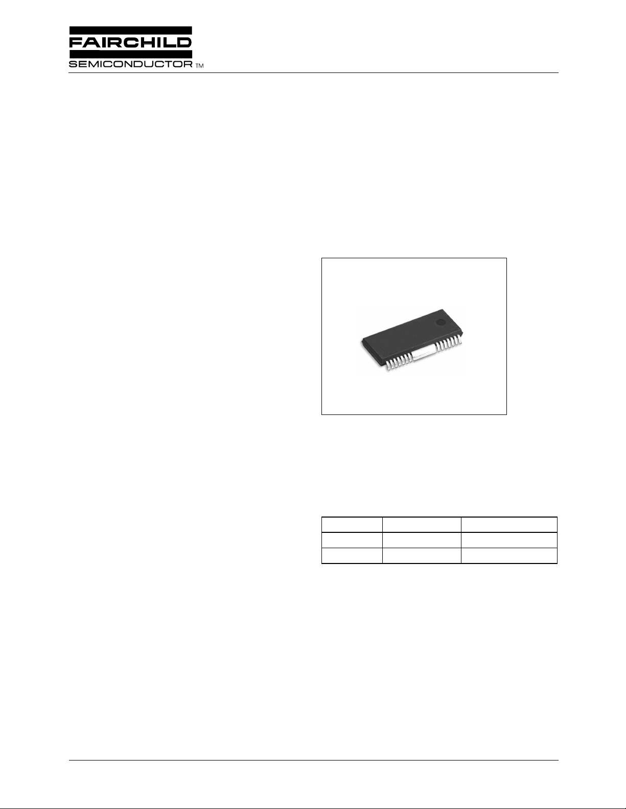
28-SSOPH-375
Typical Application
• Compact disk player (CDP)
• Video compact disk player (VCD)
• Automotive compact disk player (CDP)
©2000 Fairchild Semiconductor International
Ordering Information
Device Package Operating Temp.
KA3030D 28-SSOPH-375 −25°C ~ +75°C
KA3030DTF 28-SSOPH-375 −25°C ~ +75°C
Rev. 1.0.1
February. 2000.
1
Page 2
KA3030D
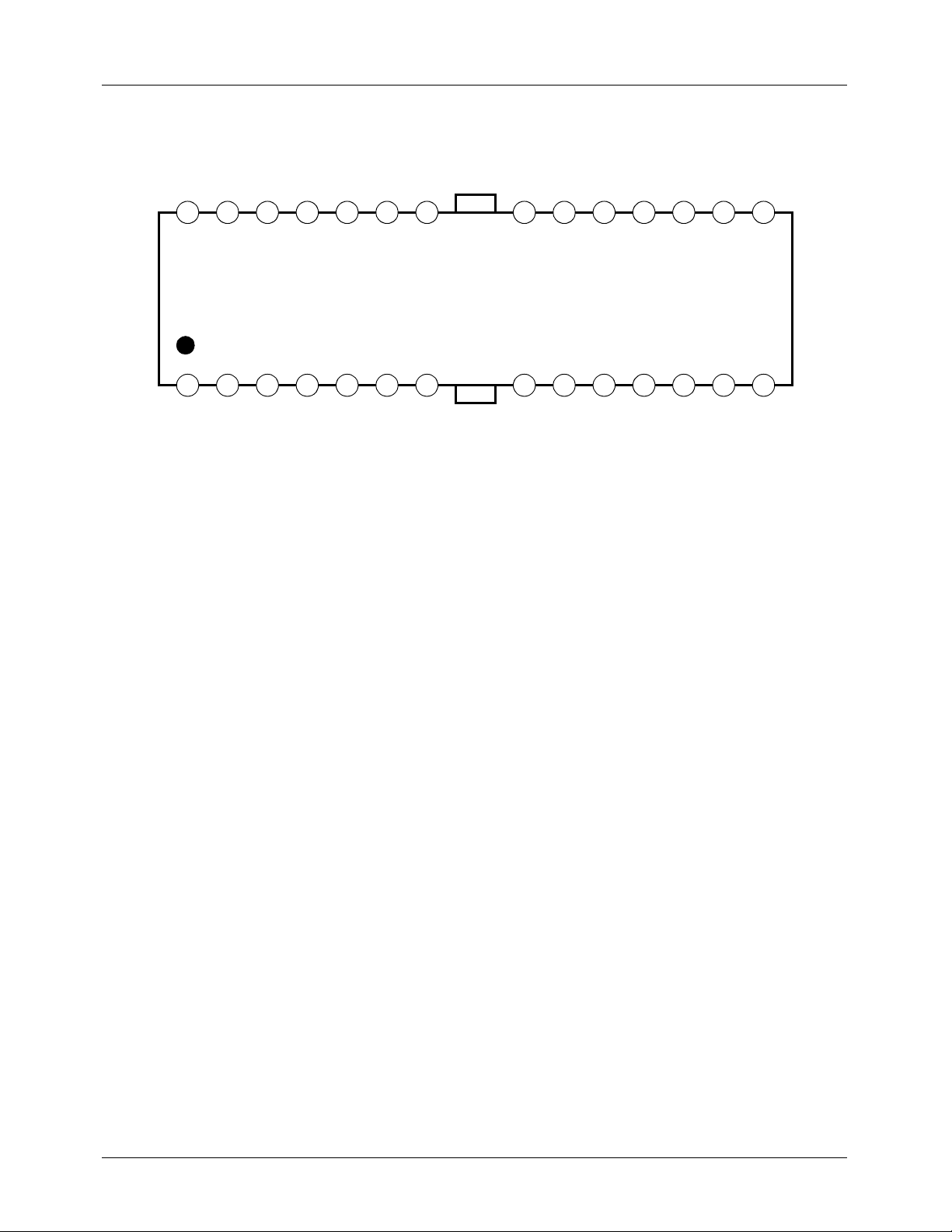
Pin Assignments
GND
DO4B
1234567 891011121314
DO1A
DO1B
DO4A
LO1A
FIN
(GND)
DI4
CTL1
REFINV
CC1
CTL2
LI2B
LI2A
DI3
DO3B
DO3A
GND
1516171819202122232425262728
KA3030D
DI1
LO1B
DI1A
FIN
(GND)
DI1B
GND
CC2
V
DI2
LO2A
LO2B
DO2A
DO2B
2
Page 3

Pin Definitions
Pin Number Pin Name I/O Pin Function Description
1 DO1A O Drive output 1A (−)
2 DO1B O Drive output 1B (+)
3 LO1A O Logic output 1A
4 LO1B O Logic output 1B
5 DI1 I Drive input 1
6 DI1A I Logic input 1A
7 DI1B I Logic input 1B
8 GND - Ground
9V
CC2
10 DI2 I Drive input 2
11 LO2A O Logic output 2A
12 LO2B O Logic output 2B
13 DO2A O Drive output 2A (+)
14 DO2B O Drive output 2B (−)
15 GND - Ground
16 DO3A O Drive output 3A (−)
17 DO3B O Drive output 3B (+)
18 DI3 I Drive input 3
19 LI2A I Logic input 2A
20 LI2B I Logic input 2B
21 CTL2 I Speed control 2
22 V
23 REF
CC1
IN
24 CTL1 I Speed control 1
25 DI4 I Drive input 4
26 DO4A O Drive output 4A (+)
27 DO4B O Drive output 4B (−)
28 GND - Ground
- Supply voltage 2
- Power supply 1
I Reference & mute input
KA3030D
3
Page 4
KA3030D
Internal Block Diagram
GND
DO4B
DO4A
DI4
CTL1
REFINV
CC1
FIN
(GND)
CTL2
LI2B
LI2A
DI3
DO3B
DO3A
GND
1516171819202122232425262728
DD
−
LEVEL SHIFT
+
LEVEL SHIFT
−
123 4567 891011121314
DO1A
+
−
−
+
DO1B
+
LO1A
SPEED CTL
LEVEL SHIFT
DDDD
LO1B
−
+
IN IN
DI1
LI1A
LI1B
SW
MUTE
BIAS
FIN
(GND)
BANGAP
REFERENCE
IN IN
LOGICLOGIC
H.V.P
T.S.D
U.V.P
GND
SPEED CTL
LEVEL SHIFT
CC2
V
DD
DI2
DD
LO2A
+
LEVEL SHIF T
−
+
−
LEVEL SHIFT
+
DD
LO2B
DO2A
−
+
−
DO2B
4
Page 5
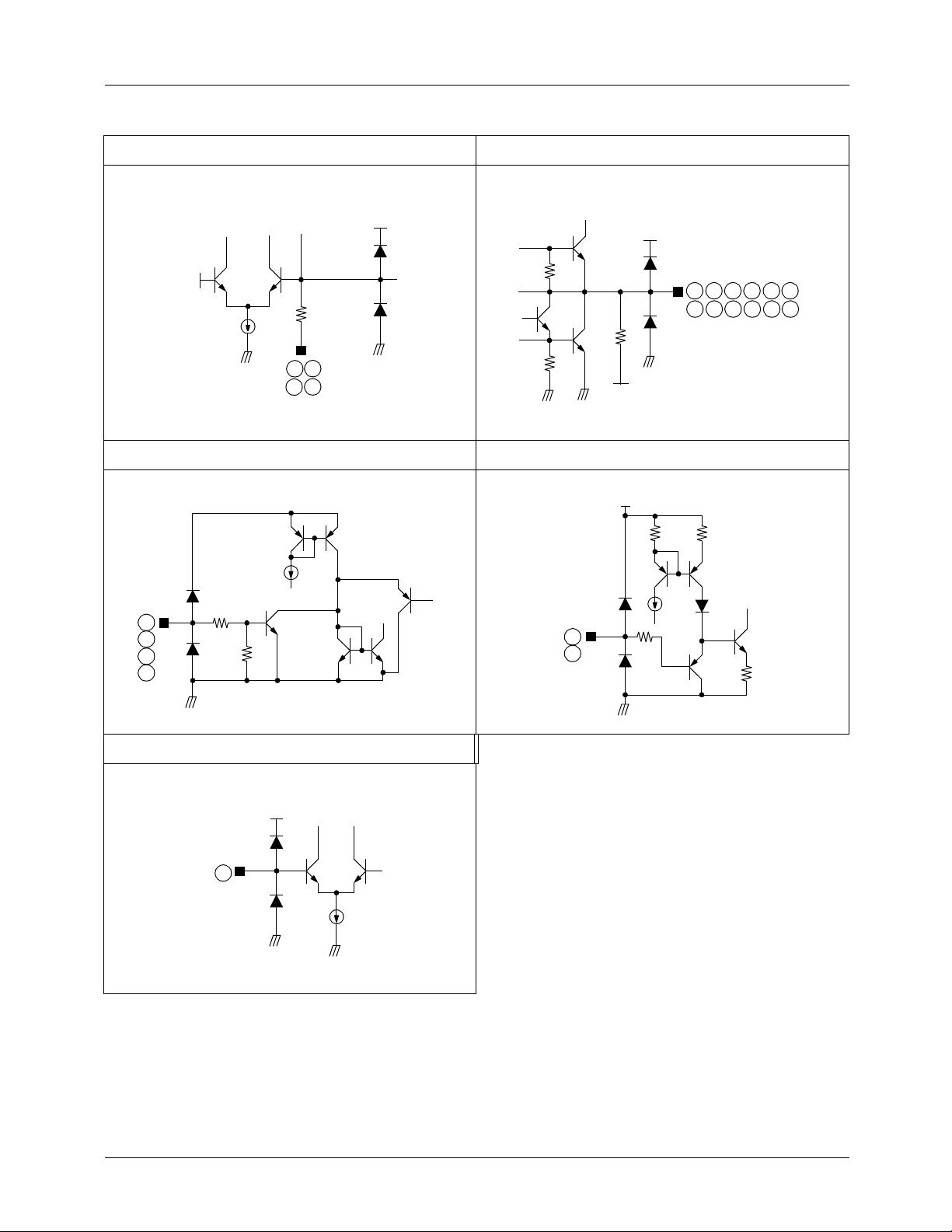
Equivalent Circuit
Driver input (Except for loading motor driver) Driver output
KA3030D
2.5V
10k
10
18
25
5
10k
0.58k
20k
V
REF1
11221331441611
26
17
27
Loading motor driver input Loading motor speed control input
6
7
19
20
10k
10k
21
24
10k
Bias
23
5
Page 6
KA3030D
Absolute Maximum Ratings (Ta = 25°°°°C)
Parameter Symbol Value Unit
Maximum supply voltage V
Power dissipation P
Maximum output current I
Operating temperature T
Storage temperature T
NOTE:
1. When mounted on 76mm ×114mm ×1.57mm PCB (Phenolic resin material).
2. Power dissipation reduces 13.6mW / °C for using above Ta=25°C
3. Do not exceed Pd and SOA.
CCMAX
D
OMAX
OPR
STG
18 V
note
1700
1A
−25 ~ 75 °C
−55 ~ 150 °C
Power Dissipation Curve
Pd (mW)
3,000
2,000
mW
1,000
0
0 25 50 75 100 125 150 175
Recommended Operating Condition (Ta = 25°°°°C)
Parameter Symbol Value Unit
Operating supply voltage
NOTE:
V
(pin 22) ≤ V
CC1
V
(pin 22) must not exceed V
CC1
CC2
(pin 9)
note
CC2
(pin 9)
V
CC
Ambient temperature, Ta [°C]
4.5 ~ 13.2 V
6
Page 7

Electrical Characteristics
(Ta=25°C, VCC=8V, unless otherwise specified)
Parameter Symbol Conditions Min. Typ. Max. Units
Quiescent circuit current I
Mute on current I
Mute on voltage V
Mute off voltage V
Under voltage protection V
High voltage protection V
CC
MUTE
MON
MOFF
UVO
HVP
FOCUS, TRACKING, SPINDLE, SLED, DRIVE PART (RL=8ΩΩΩΩ)
Input offset voltage V
Output offset voltage V
Max. output voltage 1 V
Close loop voltage gain 1 A
Max. output voltage 2 V
Close loop voltage gain 2 A
OO
OM1
VF1
OM2
VF2
Ripple rejection ratio RR V
Slew rate SR Square waveform,
LOADING, CHANGER DRIVE PART (RL=45ΩΩΩΩ)
Input high level voltage V
Input low level voltage V
Output voltage 1 V
Output voltage 2 V
O1
O2
Output load changing 1 ∆V
Output load changing 2 ∆V
Output offset voltage 1 V
Output offset voltage 2 V
OO1
OO2
Under no load 8 11 14 mA
V
=GND - 3 6 mA
PIN23
---0.5V
-2--V
---4V
-19--V
IO
- −20 - 20 mV
VIN=2.5V −40 - 40 mV
VCC=5V 2.4 3 - V
VCC=5V, VIN=0.1V
VCC=8V 4.7 5.7 - V
VCC=8V, VIN=0.1V
=0.1V
IN
, f=100Hz 40 60 - dB
RMS
Vout=3Vp-p, f=100Hz
IH
IL
RL1IL
VCC=5V, V
VCC=8V, V
=100mA→400mA,
-2--V
---0.5V
=2.5V 2.6 3.2 3.8 V
CTL
=3.5V 5.2 6.0 6.8 V
CTL
High terminal
RL2IL
=100mA→400mA,
low terminal
VIN=5V, 5V −10 - 10 mV
VIN=0V, 0V −10 - 10 mV
RMS
RMS
KA3030D
7.5 9 10.5 dB
7.5 9 10.5 dB
-0.8-V/µs
- 100 300 mV
- 100 300 mV
7
Page 8

KA3030D
Application Information
1. REFERENCE INPUT & MUTE CIRCUITS
Pin 23 can be used as a reference input terminal and a mute terminal.
• Reference input circuit
An external allowable reference voltage to pin 23 is normally 2.5V.
In general conditions, pin 23 is used as the reference input terminal and is good to be used between about
2V-6.5V.
• Mute circuit
The following represents the conditions when the external mute is permitted to pin 23.
Mute voltage Min. Typ. Max. Device condition
Mute on voltage[V] - - 0.5 Mute
Mute off voltage[V] 2 - - Operate
2. THERMAL SHUT-DOWN CIRCUIT
V
REF BG
The setting voltage of V
VBE = V
REF BG
BE
× R2 / (R1 + R2) = 400mV
Because the thermal coefficient of V
(at 25°C), V
for turning on Q becomes 400mV, and then Q turns on and the mute control cir cuit oper ates.
BE
R1
R2
(Q) is −2mV / 1°C and if TR Q reaches 175°C from its normal off state
BE
Mute control
Q
8
Page 9

3. UNDER / HIGH VOLTAGE PROTECTION CIRCUIT
V
REF BG
KA3030D
V
CC
R1
+
R2
[UNDER VOLTGE PROTECTION]
−
• [UNDER VOLTGE PROTECTION]
• Normal state: V
• Normal state: V
= 2.5V < V1 = VCC × R2 / (R1 + R2)
BGR
= V1 + V2 + V3 + V
Z
• [HIGH VOLTAGE]
• Mute state: V1 < V
• Mute state: V
CC
(VCC is below 4V)
BGR
> VZ (VCC is above 20V)
V1
Mute control
Q
V2
V3
V
R
[HIGH VOLTAGE]
Mute control
Q
R
9
Page 10

KA3030D
4. FOCUS, TRACKING, SPINDLE, SLED DRIVE CIRCUITS
M
V1’
GV2
−
+
V1
V
Rref
REF
I
C
V2’
+
−
V2
−
LEVEL SHIFTER
V
REF
(pin 23)
GV = 20log (V
) = GV1 + GV2 = 3.5dB + 6dB = 9.5dB
O/VIN
Vref is fixed to 2.5V as the external bias voltage and the input signal through the V
GV1
+ −
+
V
IN
is amplified to about 9.5dB through two
IN
state AMP.
In the level shift circuitry, the input signal is transformed into the current so that the voltage V1 and V2 are shifted to V1’ and
V2’ respectively.
V1’ = V1 + (I
V2’ = V2 − (I
Because V1 and V2 voltages, in their initial state, are equal, the voltage, V
C
C
× V
× V
) = V1 + ∆V
REF
) = V2 − ∆V
REF
, on the sides of the motor is following VM = V1’
M
− V2’ = ∆V − (−)∆V = 2∆V
Rotation occurs due to 2∆V voltage difference at both sides of the motor.
10
Page 11

5. LOADING, CHANGER DRIVE CIRCUITS
KA3030D
D
LEVEL SHIF T
SPEED
CONTROL
LOGIC
IN1
M
D
V
IN2
OUT1 OUT2
V
CTL
IN IN
V
Notes:
V
: When the motor speed control voltage is permitted between 0V ~ 4V, the motor varies its speed.
CTL
Between 4V ~ 5V, the motor can be used at constant speed and over 5.8V, the motor should not be used.
Furthermore, when V
= 5V, CTL voltage should not be permitted to exceed 3V
CC
The logic signals, input from the MCU, is inverted in the inverter and can control the changes of the output properties, that
depend on the input signal. There properties are shown in the table below.
Logic input A Pin 6, Pin 19 H H L L
Logic input B Pin 7, Pin 20 H L H L
Output type
Vr
On On
(note)
L
VrLogic output A Pin 3, Pin 11 H
Logic output B Pin 4, Pin 12 L H
Notes:
The bias voltage Vr is expressed as below;
V
–
CCVBE
Vr
--------------------------- -
V[]=
2
11
Page 12

KA3030D
c
c
c
c
g
g
g
g
Typical Performance Characteristics
Vcc vs Icc
Vcc vs Icc
Icc(mA)
12
12
1212
10
10
1010
Vcc vs IccVcc vs Icc
8888
7777
Vre(V)
Vcc vs Vreg
Vcc vs Vreg
Vcc vs VregVcc vs Vreg
8888
6666
4444
2222
0000
00002
Av(db)
16
16
1616
14
14
1414
12
12
1212
10
10
1010
8888
6666
4444
2222
0000
24
46
22
44
00006
68
66
68
89
66
88
Vcc vs Avf
Vcc vs Avf
Vcc vs AvfVcc vs Avf
89
910
88
99
910
10 11
99
1010
10 11
11 12
1010
1111
Vcc=vara*
Vpad23=2.5V
Vpad7=Vcc
11 12
12 13
1111
1212
Vcc(V)
Vcc=8V
Vpad23=2.5V
Vpad7=Vcc
IL=100mA
12 13
1212
Vcc(V)
6666
5555
4444
Vcc=vara
3333
Vpad23=2.5V
Vpad7=Vcc
2222
13
1313
00002
24
22
46
68
44
66
89
910
88
99
10 11
1010
11 12
12 13
1111
1212
13
1313
Vcc(V)
Vo1(V)
6666
5555
4444
3333
Vctl vs Vo1
Vctl vs Vo1
Vctl vs Vo1Vctl vs Vo1
Vcc=8V
Vpad23=2.5V
2222
1111
0000
13
1313
2222 2.5
2.5 3333 3.5
2.52.5
3.5 4444 4.5
3.53.5
Vpad7=Vcc
Vpad9=5V
RL=45Ohm
Vctl=Vara
4.5 5555 5.5
4.54.5
5.5 6666
5.55.5
Vctl(V)
8888
7777
6666
5555
4444
3333
2222
1111
0000
Vreg(V)
-25
-25 -12.5
-12.5 0000 12.5
-25-25
-12.5-12.5
Temp vs Vre
Temp vs Vre
Temp vs Vre
Temp vs Vre
12.5 25
25 37.5
12.512.5
2525
Vcc=8V
Vpad23=2.5V
Vpad7=Vcc
IL=100mA
37.5 50
37.537.5
50 62.5
62.5 75
5050
62.562.5
Temp(℃)
75
7575
Icc(mA)
14.00
14.00
14.0014.00
12.00
12.00
12.0012.00
10.00
10.00
10.0010.00
8.00
8.00
8.008.00
6.00
6.00
6.006.00
4.00
4.00
4.004.00
2.00
2.00
2.002.00
0.00
0.00
0.000.00
-25
-25 -13
-13 000013
-25-25
-13-13
Temp vs Ic
Temp vs Ic
Temp vs Ic
Temp vs Ic
13 25
25 38
1313
2525
38 50
3838
Vcc=8V
Vpad23=2.5V
Vpad7=Vcc
Vin=0.1Vrms
f=1K h z
50 63
63 75
5050
6363
Temp(℃)
75
7575
12
Page 13

Typical Performance Characteristics (Continued)
Temp vs Vom
Temp vs Vom
Vom(V)
10
10
1010
9999
8888
7777
6666
5555
4444
3333
2222
1111
0000
Vom(V)
7777
6666
5555
4444
3333
2222
1111
0000
-25
-25 -10
-25-25
0000 0.5
0.5 1111 1.5
0.50.5
Temp vs VomTemp vs Vom
-10 555520
-10-10
20 35
2020
Vctl vs Vom
Vctl vs Vom
Vctl vs VomVctl vs Vom
1.5 2222 2.5
1.51.5
2.5 3333 3.5
2.52.5
35 50
3535
3.5 4444 4.5
3.53.5
Vcc=8V
Vctl=3.8V
Vin=6V /0V
RL=45
2-ch logic
drive
50 65
5050
Vcc=8V
Vpad23=2.5V
RL=45
Ω
65 75
6565
temp
(℃℃℃℃)
Ω
4.5 5555
4.54.5
Vctl(V)
75
7575
Vom(V)
6666
5555
4444
3333
2222
1111
0000
4444 4.5
4.5 5555 5.5
4.54.5
Vcc vs Vom
Vcc vs Vom
Vcc vs VomVcc vs Vom
5.5 6666 6.5
6.5 7777 7.5
5.55.5
6.56.5
Vctl=3V
Vin=6V /0V
RL=45
2-ch logic
drive
7.5 8888999910
7.57.5
10 11
1010
KA3030D
Ω
11 12
12 13
1111
1212
Vcc(V)
13
1313
13
Page 14

KA3030D
Test Circuits
TRACKING
V
2.5V
1
SW5
REF
MUTE
2
CHANGER
~ ~
10µF
8 8
2
+
1
SW6
CTL1
CTL2
3
IN3
IN4
3
SLED
10µF
2
+
1
SW3
1516171819202122232425262728
KA3030D
1 2 3 4 5 6 7 8 91011121314
SW1
1
8
45
IL
IL
~
+
10µF
3
2
IN1
IN2
10µF
SPINDLE
SW2
1
3
45
+
2
~
IL IL
8
FOCUS
LOADING
14
1000µF
RIPPLE
SW4
1
2
+
+
~
VCC
100µF
Page 15

Test Circuits (Continued)
(Switch condition)
KA3030D
Parameter Symbol
Quiescent circuit current I
Mute on current I
Mute on voltage V
Mute off voltage V
Under voltage protection V
High voltage protection V
CC
MUTE
MON
MOFF
UVP
HVP
SW1 SW2 SW3 SW4 SW5 SW6
222212R
222222
222222
222222
222212
222212
Switch number
FOCUS, TRACKING, SPINDLE, DRIVE PART
Input offset voltage V
Output offset voltage V
Max. output voltage 1 V
Close loop voltage gain 1 A
Max. output voltage 2 V
Close loop voltage gain 2 A
IO
OO
OM1
VF1
OM2
VF2
222212R
222212
333213
111211
333213
111211
Ripple rejection ratio RR 333113
Slew rate SR 111211
LOADING, CHANGER DRIVE PART
Input high level voltage V
Input low level voltage V
Output voltage 1 V
Output voltage 2 V
Output load changing 1 ∆V
Output load changing 2 ∆V
Output offset voltage 1 V
Output offset voltage 2 V
IH
IL
O1
O2
RL1
RL2
OO1
OO2
222212R
222212
222212
222212
222212
222212
222212
2222-2
Remark
=∞
L
=8Ω
L
=45Ω
L
15
Page 16

KA3030D
Application Circuits
SERVO PRE-AMP CONTROLLER
FOCUS
INPUT
TRACKING
INPUT
TRACKING
REF &
MUTE
SLED
INPUT
SPINDLE
INPUT
VCC1
CHANGER
INPUT
LOADING
INPUT
CONTROL
SLED
M
INPUT
1516171819202122232425262728
KA3030D
1 2 3 4 5 6 7 8 9 10 11 12 13 14
Vcc2
FOCUS
LOADING
16
CHANGER
MMM
SPINDLE
Page 17

KA3030D
DISCLAIMER
FAIRCHILD SEMICONDUCTOR RESERVES THE RIGHT TO MAKE CHANGES WITHOUT FURT HER NOTICE TO ANY
PRODUCTS HEREI N TO IMPROVE RELIABILITY, FUNCTIO N OR DESIGN. FAIRCH IL D DOES NOT ASSUME ANY
LIABILITY ARISING OUT OF THE APPLICATION OR USE OF ANY PRODUCT OR CIRCUIT DESCRIBED HEREIN; NEITHER
DOES IT CONVEY ANY LICENSE UNDER IT S PATENT RIGHTS, NOR THE RIGHTS OF OTHE RS.
LIFE SUPPORT POL I CY
FAIRCHILD’S PR ODUCTS ARE NOT AUTH ORIZED FOR USE AS C RITICAL COMPONENT S IN LIFE SUPPORT DE VICES
OR SYSTEMS WITHOUT THE EXPRESS WRITTEN APPROVAL OF THE PRESIDENT OF FAIRCHILD SEMICONDUCTOR
INTERNATIONAL. As used herein:
1. Life support devices or systems are devices or systems
which, (a) are intended for surgical implant into the body,
or (b) support or sustain life, and (c) whose failure to
perform when properly used in accordance with
2. A critical component in any component of a life support
device or sy stem whose fai lure to perform can be
reasonably expec ted to cause the failur e of the life support
device or system, or to affect its safety or effec t iv ene ss .
instructions for use provided in the labeling, can be
reasonably expected to result in a significant injury of the
user.
www.fairchildsemi.com
12/1/00 0.0m 001
2000 Fairchild Semiconductor International
Stock#DSxxxxxxxx
 Loading...