

IXBD4410 / IXBD4411
ISOSMARTTM Half Bridge Driver Chipset
Type Description Package Temperature Range
IXBD4410PI Full-Feature Low-Side Driver 16-Pin P-DIP -40 to +85°C
IXBD4411PI Full-Feature High-Side Driver 16-Pin P-DIP -40 to +85°C
IXBD4410SI Full-Feature Low-Side Driver 16-Pin SO -40 to +85°C
IXBD4411SI Full-Feature High-Side Driver 16-Pin SO -40 to +85°C
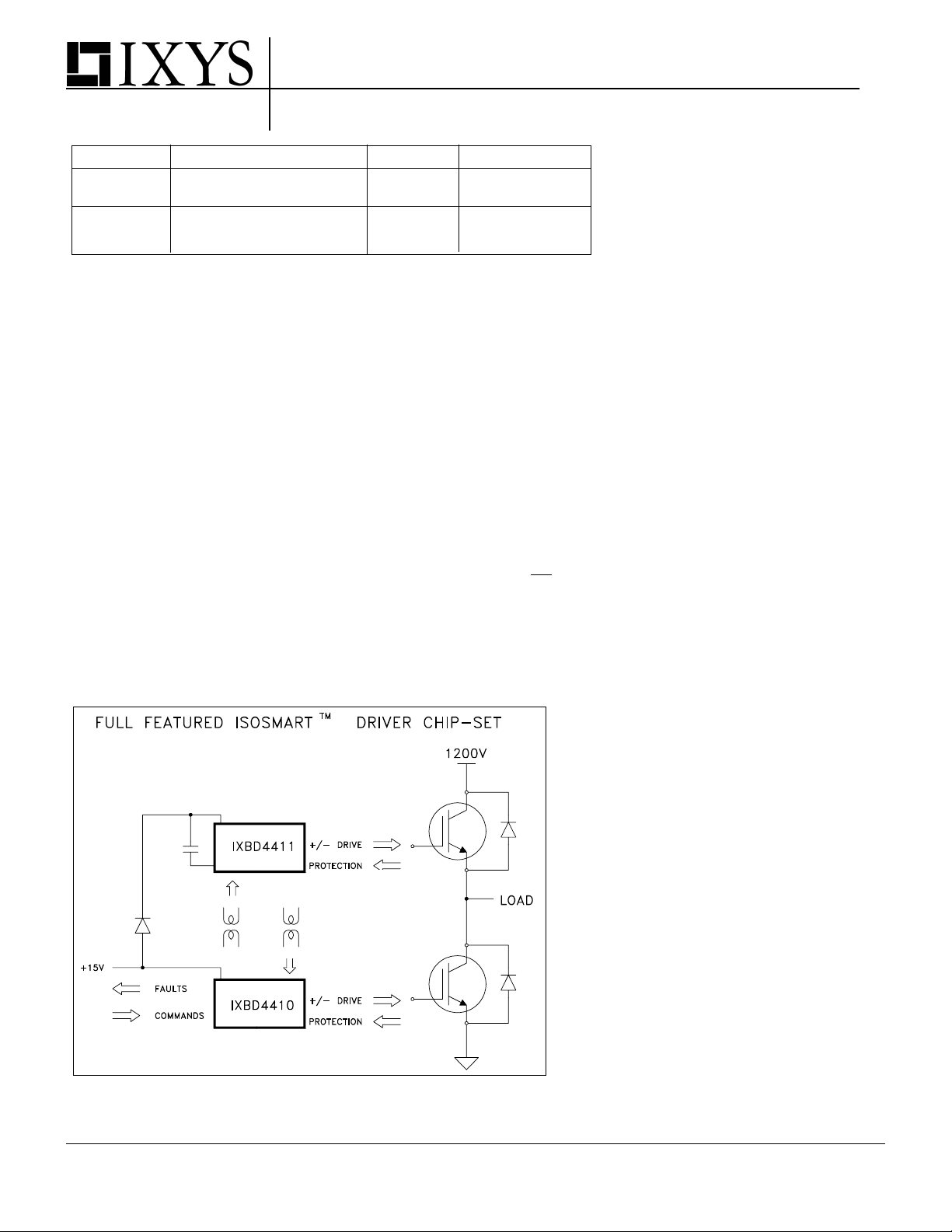
The IXBD4410/IXBD4411
ISOSMART chipset is designed to
control the gates of two Power
MOSFETs or Power IGBTs that are
connected in a half-bridge (phaseleg) configuration for driving
multiple-phase motors, or used in
applications that require half-bridge
power circuits. The IXBD4410/
IXBD4411 is a full-feature chipset
consisting of two 16-Pin DIP or SO
devices interfaced and isolated by
two small-signal ferrite pulse
transformers. The small-signal
transformers provide greater than
1200 V isolation.
Even with commutating noise
ambients greater
than ±50 V/ns and
up to 1200 V potentials, this chipset
establishes error-free two-way
communications between the
system ground-referenced
IXBD4410 and the inverter output-
referenced IXBD4411. They incorporate undervoltage V
and overcurrent or desaturation
or VEE lockout
DD
shutdown to protect the IGBT or
Power MOSFET devices from
damage.
The chipset provides the necessary
gate drive signals to fully control the
grounded-source low-side power
device as well as the floatingsource high-side power device.
Additionally, the IXBD4410/4411
chipset provides a negative-going,
off-state gate drive signal for
improved turn-off of IGBTs or Power
MOSFETs and a system logiccompatible status fault output FLT to
indicate overcurrent or desaturation,
and undervoltage V
a status fault, both devices drive
or VEE. During
DD
their respective gate outputs at VEE,
and keep their driven MOSFETs or
IGBTs off.
Features
● 1200 V or greater low-to-high side
isolation.
● Drives Power Systems Operating on
up to 575 V AC mains
● dv/dt immunity of greater than
±50V/ns
● Proprietary low-to-high side level
translation and communication
● On-chip negative gate-drive supply
to ensure Power MOSFET or IGBT
turn-off and to prevent gate noise
interference
● 5 V logic compatible HCMOS inputs
with hysteresis
● Available in either the 16-Pin DIP or
the 16-Pin wide-body, small-outline
plastic package
● 20 ns switching time with 1000 pF
load; 100 ns switching time with
10,000 pF load
● 100 ns propagation delay time
● 2 A peak output drive capability
● Self shut-down of output in response
to over-current or short-circuit
● Under-voltage and over-voltage V
lockout protection
● Protection from cross conduction of
DD
the half bridge
● Logic compatible fault indication
from both low and high-side driver
540 V-
IXYS reserves the right to change limits, test conditions and dimensions.
I - 1
Applications
● 1- or 3-Phase Motor Controls
● Switch Mode Power Supplies
(SMPS)
● Uninterruptible Power Supplies
(UPS)
● Induction Heating and Welding
Systems
● Switching Amplifiers
● General Power Conversion Circuits
© 2001 IXYS All rights reserved
IXBD4410 / IXBD4411
Symbol Definition Maximum Ratings
VDD/V
EE
V
in
I
in
Io (rev) Peak Reverse Output Current (OUT) 2 A
P
D
Supply Voltage -0.5 to 24 V
Input Voltage (INH, INL) -0.5 to VDD+0.5 V
Input Current (INL, INH, IM) ±10 mA
Maximum Power Dissipation (TA ≤ 25°C)
16 Pin PDIP (PI) 1.6 W
16 Pin SOIC (SI) 1.2 W
θθ
θ
θθ
JA
Thermal Impedance (Junction To Ambient)
16 Pin PDIP (PI) 75 °C/W
16 Pin SOIC (SI) 100 °C/W
T
A
T
JM
T
stg
T
L
Operating Ambient Temperature -40 to +85 °C
Maximum Junction Temperature +150 °C
Storage Temperature Range -55 to +150 °C
Lead Soldering Temperature for 10 s 300 °C
Recommended Operating Conditions
V
DD/VEE
VDD/LG 10 to 16.5 V
LGh/L
Gl
Supply Voltage 10 to 20 V
Maximum Common Mode dv/dt ±50 V/ns
Symbol Definition/Condition Characteristic Values
= 25°C, VDD = 15 V, unless otherwise specified)
(T
A
min. typ. max.
Dimensions in inch (1" = 25.4 mm)
16-Pin SO
INL, INH Inputs (referred to LG)
V
t+
V
t-
V
ih
I
in
C
in
Positive-Going Threshold 3.65 V
Negative-Going Threshold 1.5 V
Input Hysteresis .6 V
Input Leakage Current/Vin=VDD or LG -1 1 µA
Input Capacitance 10 p F
Open Drain Fault Output (referred to LG)
V
oh
V
ol
HI Output/Rpu = 10 kΩ to V
DD
LO Output/Io = 4 mA 0.4 0.7 V
OUT Output (referred to LG)
V
oh
V
ol
R
o
R
o
I
pk
HI Output/Io = -5 mA VDD-0.05 V
LO Output/Io = 5 mA VEE+0.05 V
Output HI Res./Io = -0.1 A 3 5 Ω
Output LO Res./Io = 0.1 A 3 4 Ω
Peak Output Current/CL = 10 nF 1.5 2 A
IM Input (referred to KG)
V
t+
C
in
R
s
Positive-Going Threshold 0.24 0.3 0.36 V
Input Capacitance 10 p F
Shorting Device Output Resistance 80 12 0 150 Ω
16-Pin Plastic DIP
VDD-0.05 V
Cross view
VEE Supply (referred to LG)
V
EE
I
out
f
inv
V
EEF
Output Voltage/Io = 1 mA, Co = 1 µF -5 -5.5 -6.5 V
Output Current/V
Inverting Frequency 35 0 kHz
Undervoltage Fault Indication -4 -4.8 V
I - 2
= 0.70 • V
out
EE
-20 -25 mA
© 2001 IXYS All rights reserved
Symbol Definition/Condition Characteristic Values
(Fig. 1A, T
= 25°C, VDD = 15 V, unless otherwise specified)
A
min. typ. max.
VDD Undervoltage Lockout
V
uv
V
uh
Drop Out 9.5 10.5 11.5 V
Hysteresis 0.1 0.3 0.5 V
Quiescent Power Supply Current
V
I
DD
Current/Vin=VDD or LG, Io = 0 3 8 mA
DD
INL and INH Inputs (Fig. 2a, 2b))
t
d(on)
t
r
t
d(off)
t
f
t
dlh(off)
t
dlh(on)
Turn-on delay time; CL =1nF 250 275 ns
4410
Rise time; CL =10 nF 70 100 ns
4410 or 4411 C
=1 nF 15 20 ns
L
Turn-off delay time CL =1nF 150 175 ns
4410
Fall time CL =10nF 70 150 ns
CL =1nF 15 20 ns
4410 to 4411
Turn-off delay time CL =1nF 250 275 ns
4410 to 4411
Turn-on delay time CL =1nF 270 300 ns
Fault Output Delay for any Fault Conditions (4410/4411)
t
FLT
FLT Delay/R
= 2 kΩ CL = 20 pF 2 3 us
pu
IXBD4410 / IXBD4411
15
OUT
IXBD4410
or
IXBD4411
R2
9
Im
Fig. 1a Overcurrent Detection
VOUT
IXBD4410
or
IXBD4411
5V
VIN
Fig. 1b Overcurrent Delay
R1
to c
4.7K
4.7K
50%
90%
CL
V IN
15V
-5V
+5V
0V
Overcurrent Protection Delay
t
oc
+15V
Driver-Off delay time CL = 10 nF 200 300 ns
(Fig. 1a, 1b)
16
1
Vdd
8
FLT
U2
3
INH
IXBD4411
2
22nF
22nF
INL
(HIGH SIDE)
9
Im
10
KG
11
LG
T+
5
22nF
22
4.7
Ω
7
16
R+
Vdd
1
U1
IXBD4410
8
FLT
(LOW SID E)
3
INH
2
INL
KG Im
LG
11
10 9
+
F
u
uF
7
.
.1
4
.1uF
Ω
T-
46
6
R-
R- R+
22
4
T- T+
OUT
CA
CB
Vee
7
Ω
5
OUT
CA
CB
Vee
1N5817
15
13
12
14
22nF
15
13
12
14
68
.1uF
7
1
8
5
N
1
4.7
68
Ω
.1uF
Fig. 2a: IXBD4410/4411 Switching time test circuit
Ω
F
u
1
.
+
22nF
Ω
22nF
.1uF 4.7uF
+
(IX B D 44 1 0 )
IN L
CL
F
u
7
.
4
+15V
OUT
LOW SID E
-5 V
tr
-5 0%
-9 0%
tf
-1 0%
td (of f)td (on )
(IX BD 4 4 1 0 )
IN H
+15V
CL
OUT
HIGH SIDE
-5 V
(IX B D 44 1 1 )
tf
td lh (o ff)
-5 0%
-
90%
-1 0%
tr
td lh (o n)
Fig. 2b: Output signal waveform
© 2001 IXYS All rights reserved
I - 3
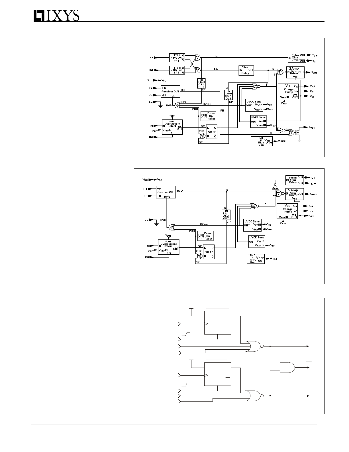
Chipset Overview
This ISOSMARTTM chipset is a pair of
integrated circuits providing isolated
high- and low-side drivers for phase-leg
motor controls, or any other application
which utilizes a half bridge, 2- or 3phase drive configuration. They consist
of two drive control inputs (INL and
INH) for two Power-MOSFET/IGBT
gate-drive outputs. Both inputs operate
from a common ground and are
activated by HCMOS compatible logic
levels. The low-side output operates
near input ground, while the high-side
output operates from a floating ground
that is nominally the source connection
of the high-side phase-leg power
device. Both outputs typically provide
2A of transient current drive for fast
switching of the phase-leg power
device.
IXBD4410 / IXBD4411
Fig. 3: IXBD4410, low-side driver block diagram
IXBD4410/IXBD4411
The full featured ISOSMART
TM
driver
chipset incorporates an IXBD4410 as
the low-side driver (Fig. 3) and an
IXBD4411 as the high-side driver (Fig.
4). When input "INL" is set to a positive
logic level, the low-side gate output
goes high (turns on); when "INH" is set
to a positive logic level, the high-side
gate drive output goes high. The highside IC is isolated from the low-side IC
by a magnetic barrier, across which the
turn on/off signal is transmitted to the
high-side gate drive. The IXBD4411
fault signal is also transmitted back to
the IXBD4410 driver via these
transformers. This isolation only
depends on the low cost communications transformer, which is designed to
withstand 1200 V or more.
There are two magnetic transmission
channels between the low- and highside IC's for bi-directional communication. One sends a signal from the
low-side IXBD4410 IC up to the highside IXBD4411 IC and the other sends
a signal back from the high-side to the
low-side IC. The signal that is sent up
controls the IXBD4411 gate-drive
output. The signal sent from the
IXBD4411 back to the IXBD4410
indicates a high-side fault has occurred
(overcurrent, or under-voltage of the
high-side + power supplies). This is
detected at the IXBD4410 driver and
sets "FLT" pin low, to indicate the highside fault.
Fig. 4: IXBD4411, high-side driver block diagram
VCC
OVER CURRENT
INH
VDD UNDE R VOLTAGE
VEE UN DE R VO LTAGE
VC C
OVER CURRENT
INL
VDD UNDE R VOLTAGE
VEE UN DE R VO LTAGE
HIGH SIDE
D
R
LO W S ID E
D
R
Q
Q
Q
Q
HIGH-SIDE
OUTPUT ENABLE
FLT
LO W-SIDE
OUTPUT ENABLE
The fault signal that is returned from
I - 4
Fig. 5: Logic Representation of IXBD4410 FLT Signal
© 2001 IXYS All rights reserved

IXBD4410 / IXBD4411
the IXBD4411 is strictly for status only.
Any gate-drive shutdown because of a
high-side fault is done locally within the
high-side IXBD4411. The IXBD4411 gatedrive will turn-off the power device
whenever an overcurrent or under voltage
condition arises. The overcurrent sensing
is active only while the gate driver output
is "high" (on). The overcurrent fault
condition is latched and is reset on the
next INH gate input positive transition. The
FLT (pin 8) of the IXBD4411 is not used
and should be grounded.
The low-side IXBD4410 driver provides
an output pin 8 (FLT) to indicate a highside
(IXBD4411) or a low-side (IXBD4410)
fault. This output pin is an "open-drain"
output. The IXBD4410 low-side driver fault
indications are similar to the IXBD4411
high-side driver indications as outlined
above. A "graphic" logic diagram of the
chipset's FLT function is presented in Fig.5.
Note that this diagram presents the logic of
this function at the "low-side" IXBD4410
driver and is not the actual circuit. It
describes the combined logic of the "fault
logic" and "hi-side fault sense" blocks in
both the IXBD4410 and IXBD4411 as
shown in Fig. 3 and 4.
The most efficient method of providing
power for the high-side driver is by
bootstrapping. This method is illustrated in
the Fig. 7 application example by diode D1
and capacitor C1. Using this method, the
power is drawn through a high-voltage
diode onto a reservoir capacitor whenever
the floating high-side ground returns to near
the real ground of the low-side driver. When
the high-side gate is turned on and the
floating ground moves towards a higher
potential, the bootstrapping diode backbiases, and the high-side driver draws its
power solely from the reservoir capacitor.
Power may also be provided via any
isolated power supply (usually an extra
secondary on the system housekeeping
supply switching transformer).
Both the IXBD4410 and IXBD4411
contain on-board negative charge pumps
to provide negative gate drive, which
ensures turn-off of the high- or low-side
power device in the presence of currents
induced by power device Miller capacitance or from inductive ground transients.
These charge pumps provide -5 V relative
to the local driver ground when V
+15 V, and at rated average currents of 25
DD
is at
mA. The charge pump requires two external
capacitors, C7 and C11 in Fig. 7. The
charge pump frequency is nominally 350
The charge pump clock is turned off
kHz.
whenever the difference between the V
and VEE supplies exceed 20 V, to prevent
DD
exceeding the breakdown rating of the IC.
Both the IXBD4410 and IXBD4411 drivers
possess two local grounds each, a
common logic ground, and "Kelvin"
ground. The Kelvin ground and logic
grounds are first connected directly to
each other, and then to the Kelvin-source
of the power device for accurate overcurrent measurement in the presence of
inductive transients on the power device
source terminal.
Power MOSFET or IGBT overcurrent
sensing utilizes an on-chip comparator
with a typical 300 mV threshold. In a
typical application, the current mirror pin
of the Power MOSFET or IGBT is connected to a grounded, low-value resistor,
and to the overcurrent comparator input
on the high- or low-side driver. The
comparator will respond typically within 200
ns to an overcurrent condition to shutdown
the driver output. The power switches
could be protected also by desaturation
detection (see Fig. 7 and 8).
To assure maximum protection for the
phase-leg power devices, the chipset
incorporates the following Power
MOSFET and IGBT protection circuits:
● Power device overcurrent or desa-
turation protection. The IXBD4410/4411
will turn off the driven device within
200ns of sensing an output overcurrent
or desaturation condition.
● Gate-drive lockout circuitry to prevent
cross conduction (simultaneous
conduction of the low- and high-side
phase-leg power devices), either under
normal operating conditions or when a
fault occurs.
● During power-up, the chipset's gate-
drive outputs will be low (off), until the
voltage reaches the under-voltage trip
point.
● Under-voltage gate-drive lockout on
the low- and/or high- side driver whenever the respective positive power
supply falls below 9.5 V typically.
● Under-voltage gate-drive lockout on
the low- and high- side driver
whenever the respective negative
power supply rises above -3 V
typically.
© 2001 IXYS All rights reserved
I - 5

IXBD4410 / IXBD4411
Pin Description
IXBD4410 (Low-Side Driver)
Sym. Pin Description of IXBD 4410/4411
VDD 1 Positive power supply.
16
INL 2 Logic input signal referenced to
NC LG (logic ground). In the
IXBD4410. A "high" to this pin
turns on its gate drive output
and resets its fault logic. A "low"
to this pin turns off the gate drive
output. In the IXBD4411 this pin
is not used and should be
connected to its ground (LG).
No Connection (IXBD 4411)
INH 3 Logic input signal referenced to
NC LG (logic ground). In the
IXBD4410, this signal is
transmitted to the IXBD4411
"high-side" driver through pins 4
and 5 (T- and T+). A "high" to
this pin turns on the IXBD4411
gate drive output and resets its
fault logic. A "low" to this pin
turns off the IXBD4411 gate
drive output. In the IXBD4411
this pin is not used and should
be connected to its ground (LG).
No Connection (IXBD 4411)
T- 4 Transmitter output complemen-
T+ 5 tary drive signals. Direct drive of
the low signal transformer, which
is connected to the receiver of
the chipset's companion device.
In the IXBD4410, this signal
transmits the on/off command to
its companion IXBD4411. In the
IXBD4411, this signal transmits
the fault indication to its
companion IXBD4410 driver.
R- 6 Receiver input complementary
R+ 7 signal. Directly connected to the
low signal transformer, which is
driven by the chipset's companion device. In the IXBD4410,
this input receives the fault
indication from its companion
IXBD4411 driver. In the
IXBD4411, this input receives
the on/off command from its
companion IXBD4410 driver.
Pin Description
IXBD4411 (High-Side Driver)
VDD VDD
NC OUT
NC VEE
T- C A
T+ CB
R- LG
R+ KG
NC IM
Sym. Pin Description of IXBD 4410/4411
FLT 8 Low/high side fault output. In the
NC IXBD4410, this output indicates
IM 9 Current sense or desaturation
KG 10 Kelvin ground. This ground is
LG 11 Logic and power ground.
CB 12 Capacitor terminals for negative
CA 13 terminal is CB (pin 12).
VEE 14 Negative supply terminal.
OUT 15 Gate drive output. In the
a fault condition of either device
of the chipset. A "high" indicates
no fault, A "low" indicates that
either overcurrent,V
under-voltage occurred. In case
DD
or V
EE
of overcurrent, this output will
remain active "low" until the next
input cycle of the respective
driver. In case of under-voltage,
this output will remain "low" until
the proper voltage is restored.
The IXBD4411 does not have a
FLT output,and its pin 8 should
be tied to LG
No Connection (IXBD 4411)
detection input. This input is
active only while the OUT pin is
"high" (on). When the OUT pin is
"low" (off) this input is pulled to
ground through a 70 Ω resistor.
Any voltage at this pin above the
threshold of .3 V typical, will turn
the output (pin 15) off. This pin is
used for power device
overcurrent protection.
used as Kelvin connection for
overcurrent or desaturation
sensing.
charge pump (VEE); "+"
IXBD4410 this output responds
to the INL signal. A "high" at INL
will turn it on ("high"), a "low" will
turn it off ("low"). In the
IXBD4411, this output responds
to the transmitted signal from the
companion IXBD4410. A "high"
at INH of the IXBD4410 drives
will turn it on ("high"). A "low"
will turn it off ("low"). This output
will turn off ("low") also in
response to any fault condition.
I - 6
© 2001 IXYS All rights reserved

IXBD4410 / IXBD4411
Application
The IXBD4410/4411 chipset devices
are specifically designed as MOSgated transistor drivers in half-bridge
power converters, 1- and 3-phase
motor controls, and UPS applications.
The phase-leg PWM command is
normally generated by previous (user
provided) circuitry. It must be
decomposed into two separate logic
signals, one for the high-side and one
for the low-side power transistors, with
appropriate deadtime for each state
transition. The deadtime insures nonoverlapping conduction even if the turnon and turn-off delay times of the
power devices are unequal. The
minimum deadtime should be greater
than t
device like the IXYS deadtime
generator IXDP630, (fig. 7), can be used
to perform this function. The
ISOSMART™ chipset family of devices
do not generate deadtime, although
there is an internal lockout that
prohibits one device form being
commanded "on" before the other is
commanded "off". This simplifies startup and shutdown protection circuitry,
preventing logic error during power-up
from turning on both high-and low-side
transistors simultaneously.
Negative V
Design
The on-chip V
the IXBD4410/4411 generates a negative power supply, regulated at 20 V
below the positive VDD rail. If VDD is +10
V, VEE will be -10 V. If VDD is +15 V, V
will be -5 V. This negative drive potential in the off-state is either desirable or
required in many instances. When
switching a clamped inductive load
(Fig. 6), the turn-on of Q2 will commutate
the freewheeling diode around Q1.
Whether this diode is intrinsic (as in a
MOSFET) or extrinsic (IGBT or
bipolar), its reverse recovery is critical
to proper circuit operation.
At high turn-on di/dt in Q2 and near its
rated voltage, the recovery of D1 can
get quite "snappy" (the di/dt in the
second half of the recovery process,
after the diode has begun to recover its
blocking capability, can get very large),
creating a very high dv/dt across Q1.
This dv/dt is impressed across the
Miller capacitance of Q1, forcing a
large current to flow out the gate
A separate circuit, or an IC
dlh.
Charge Pump Circuit
EE
generator provided in
EE
EE
failure, this problem is even more likely
to occur. In an industrial module package
(e.g.: a 150 A/1200 V IGBT phase-leg
module), the series inductance contributed by the long gate leads and
connectors further complicate the design.
In a heavily snubbered converter, or in
a power supply design with low
transformer leakage inductance, the
design problem is relatively simple and
negative drive is seldom required.
However, in a modern snubberless or
lightly snubbered converter design, it is
important to keep the gate drive
impedance high enough during
transistor turnoff to limit the reapplied
dv/dt (the transistor is its own 'active'
snubber). This is always important for
EMI control, and in the case of IGBT
may be required to achieve the
necessary RBSOA. At the same time, it
is mandatory to keep the off-state gate
Fig. 6: Switching a clamped inductive
load
drive impedance very low to assure the
transistor remain off during induced
dv/dt (including diode recovery dv/dt).
terminal of the device. If this current pulse
causes a high enough voltage drop
across the output impedance of the gate
drive circuit, R
, Q1 will be turned on.
out
The Q1 conduction in every instance
Q2 is turned on (and vice versa), aside
from degrading efficiency, can lead to
catastrophic failure of both power
transistors. At high temperature, where
In some instances, it is simply not
possible to satisfy both criteria with 0 V
applied in the off-state. In these cases
the IXBD4410/4411 with V
bias generator must be used.
The internal V
pump circuit. Referring to Fig. 7, an
generator is a charge
EE
negative
EE
external charge pump capacitor is
required between the CA and CB
the -6 to -7 mV/°C temperature
coefficient of IGBT/MOSFET threshold
reduces the voltage required to create a
Fig. 7: IXBD4410/4411 Detailed one phase circuit with dead time generator IXDP 630
© 2001 IXYS All rights reserved
I - 7

IXBD4410 / IXBD4411
terminals (C7, C11), and an output
reservoir capacitor between V
GND (C10, C14). A 0.1 µF charge
EE
and
pump capacitor (C7, C11) is recommended. The voltage regulation
method used in the IXBD4410/4411
allows a 1 to 2 V ripple frequency and
depends on the size of the V
reservoir capacitor (C10, C14) and the
output
EE
average load current. The minimum
recommended output reservoir (C10,
C14) is 4.7 µF tantalum, or 10 µF if
aluminium electrolytic construction is
chosen. Note that this reservoir
capacitor is in addition to a good
quality high frequency bypass capacitor (0.1 µF) that should be placed from
VEE to GND (C9, C13).
A small resistor in series with the
charge pump capacitor, (R7, R8)
reduces the peak charging currents of
the charge pump. A value or 68 Ω or
greater is recommended, as illustrated
in the applications example in Fig. 7.
Current Sense / Desaturation
Detection Circuit
All members of the ISOSMART™
driver family provide a very flexible
overcurrent/short circuit protection
capability that will work with both
standard three-terminal power transistors,
and with 4- and 5-terminal current sensing
power devices. Overcurrent detection is
accomplished as illustrated in Fig. 8a (for
a current mirror power device) and Fig.
8b (for a standard three terminal power
transistor). Desaturation detection is
accomplished with the same internal
circuits by measuring the voltage across
the power transistor in the on-state with
an external resistor divider (Fig. 8c).
The IM input trip point V
300 mV, is referenced to the Kelvin
, typically
TIM
ground pin KG.
Current Mirror
MOSFET and IGBT allow
good control of peak let-through
currents and excellent short circuit
protection when combined with the
ISOSMART™ driver family of devices.
The sense resistor is chosen to
develop 300 mV at the desired peak
transistor current, assuming a mirror
ration of 1400:1, and a trip point of 30
A is desired:
= 300 mV • 1400/30 A = 14 Ω
R
s
(use 15 Ω CC).
It is important to realize that C
unit area of the mirror cells is much larger
oss
per
a b c
IM
KG
GND
With Current Mirror
R
s
IM
KG
GND
With Standard
MOSFET/IGBT
Fig. 8: Alternative overcurrent protection circuits
that C
chip due to periphery effects. This
per unit area of the bulk of the
oss
causes a large transient current pulse at
the mirror output whenever the transistor
switches (C • dv/dt currents), which can
cause false overcurrent trigger. The RC
filter indicated in Fig. 8a will eliminate this
problem.
Standard three-terminal MOSFET and
IGBT devices (in discrete as well as
modern industrial single transistor and
phase-leg modules) can also be
protected from short circuit with the
ISOSMART™ driver family devices. In
discrete device designs, where the
source/emitter terminal is available,
overcurrent protection with an external
power resistor can be implemented.
The resistor is placed in series with the
device emitter, with the full device
current flowing through it (Fig. 8b). The
sense resistor is again selected to
develop 300 mV at the desired peak
transistor current, assuming a trip point
of 30 A is desired:
= 300 mV / 30 A = 10 mΩ
R
s
(use 10 mΩ, noninductive
current sense resistor).
It is important to recognize that
"noninductive" is a relative term,
especially when applied to current
sense resistor construction and
characterization. There is always
significant series inductance inserted
with the sense resistor, and L • di/dt
voltage transients can cause false
overcurrent trigger.
The RC filter indicated in Figure 8b will
eliminate this problem. Choosing the
RC pole at the current sense resistor
RL zero should exactly compensate for
series inductance. Because the exact
value is not normally known (and can
vary depending on PC layout and
component lead dress) this is not
normally a good idea. Usually, the RC
R
IM
s
KG
GND
Desaturation Detection
with Standard
MOSFET/IGBT
R
s
time constant should be two to ten
times longer than the suspected RL
time constant.
Desaturation detection as in Figure 8c is
probably the most common method of
short circuit protection in use today.
While not strictly an "overcurrent"
detector, if the power transistor gain,
and consequently short circuit letthrough current, is well controlled (as
with modern MOSFET and IGBT) this
methodology offers very effective
protection.
The IXBD4410/4411 half-bridge circuits
in Fig. 7 uses desaturation detection. In
Fig. 7, the voltage across the two power
MOSFET devices (or IGBTs) are
monitored by two sets of voltagedivider networks, R10 and R11 for the
high-side gate driver, and R13 and R14
for the low-side gate driver. The
dividers are set to trip the IM input
comparators when either Power
MOSFET device V
reasonable value, perhaps 50 V
exceeds a
DS
(usually a value of 10 % of the nominal
DC bus voltage works well). R10 or
R13 are chosen to tolerate the applied
steady state DC bus voltage at an
acceptable power dissipation. Dielectric
withstand capability, power handling,
temperature rise, and PC board creep
and strike spacings, must all be
carefully considered in the design of
the voltage-divider networks.
In the off-state, the voltage across the
Power MOSFET device may go as high
as the DC bus potential. To keep this
normal condition from setting the
internal fault flip-flop of the IXBD4410
or the IXBD4411, an internal CMOS
switch is turned on and placed across
lM and KG pins shorting them together.
This effectively discharges C8 or C12
in Fig. 7 and maintains zero potential with
respect to KG at IM.
I - 8
© 2001 IXYS All rights reserved

IXBD4410 / IXBD4411
When the command arrives to switch
on the Power MOSFET device, the
CMOS switch shorting IM to KG is
turned off. The driven Power MOSFET
device is switched on approximately
100 ns to 1 µs later, and with typical
load conditions, its drain-to-source
potential, V
10 µs of delay to collapse to the normal
, may take an additional
DS
on-state voltage level. To prevent false
triggering due to this, C8 or C12 in
parallel combination with R10 and R11,
or R13 and R14, delays the IM input
signal. During this turn-on interval, the
voltage across C8 or C12 will rise until
the Power MOSFET device finally
comes on and pulls the voltage across
C8 or C12 back down. If the MOSFET
device load circuit is shorted, its V
voltage cannot collapse at turn-on. In
DS
this case, the voltage across C8 or C12
rises rapidly until it reaches 300 mV,
tripping the fault flip-flop and shutting
down the driver output. At the same
time, C8 or C12 must be kept small
enough that the added delay does not
slow down the detection of a short
circuit event so much that the Power
MOSFET device fails before the driver
realizes that it is in trouble. The
desaturation detection circuit in Fig. 7
functions as just described. Current limit
or desaturation detection is latched, and
reset on a cycle-by-cycle basis with the
rising edge of the respective input
command.
100 A in a typical application). Fig. 7 is
a detailed schematic of one phase of
three 3-phase motor control, showing
the interconnection of the IXBD4410/
4411 and its associated circuitry.
PCB Layout Considerations
The IXBD4410/4411 is intended to be
used in high voltage, high speed, high
dv/dt applications.
To ensure proper operation, great care
must be taken in laying out the printed
circuit board. The layout critical areas
include the communication links, current
sense, gate drive, and supply bypassing.
The communication path should be as
short as possible. Added inductance
disturbs the frequency response of the
signal path, and these distortions may
cause false triggering in the receiver.
The transformer should be placed
between the two ICs with the orienta-
tion of one IC reversed (Fig. 10).
Capacitance between the high-side
and low-side should be minimized. No
signal trace should run underneath the
communication path, and high- and lowside traces should be separated on the
PCB. The dv/dt of the high-side during
power stage switching may cause false
logic transitions in low-side circuits due
to capacitive coupling.
The low signal pulse transformer
provides the isolation between high-
Three Phase Motor Controls
Fig. 9 is a block diagram of a typical 3phase PWM voltage-source inverter
motor control. The power circuit consists
of six power switching transistors with
freewheeling diodes around each of
them. The control function may be
performed digitally by a microprocessor,
microcontroller, DSP chip, or user custom
IC; or it may be performed by a PC
board full of random logic and analog
circuits. In any of these cases, the PWM
command for all six power transistors is
generated in one circuit, and this circuit is
usually referred to system ground
potential - the bottom terminal of the
power bridge.
The ISOSMART™ family of drivers is
the interface between the world of control
logic and the world of power, 5 V input
logic commands precisely control actions
at high voltage and current (1200 V and
Fig. 9: Typical 3-phase motor control system block diagram
© 2001 IXYS All rights reserved
I - 9

IXBD4410 / IXBD4411
low-side circuits. For 460 V~ line
operation, a spacing of 4 mm is recommended between low- and high-side
circuits, and a transformer HIPOT
specification of at least 1500 V~ is
required. This creep spacing is usually
adequate to control leakage currents on
the PCB with up to 1200 V~ applied
after 10 to 15 years of accumulated dust
and particulates in a standard industrial
environment. In other environments, or
at other line voltages, this spacing
should be appropriately modified.
Fig. 10: Suggested IC Orientation
Power Circuit Noise Considerations
In a typical transistor inverter, the output
MOSFET may switch on or off with di/dt
>500 A/µs. Referring to Fig.11 and
assuming that the MOSFET source
terminal has a one inch path on the
PCB to system ground, a voltage as
high as V = 27 nH • 500 A/µs = 13.5 V
can be developed. If the MOSFET
switched 25 A, the transient will last as
long as (25/500) µs or 50 ns, which is
more than the typical 6 or 7 ns propagations or of a 74HC series gate.
while positioning the transistors next
to their heat sink and meeting UL/VDE
voltage spacings is just too difficult.
Grounding the gate driver as in option
(a) in Fig. 11 solves the MOSFET turn
on problem by eliminating LS1 from the
source feedback loop. Now, unfortunately, the gate driver will oscillate
every time it is turned on or off. As the
IXDP630 output goes "high", the gate
drive output follows (after its propagation delay) and the MOSFET starts to
conduct. The voltage transient induced
The current sense/desaturation detect
input is noise sensitive. The 300 mV trip
point is referred to the KG (Kelvin
ground) pin, and the applied signal must
be kept as clean as possible, A filter is
recommended, preferably a monolithic
ceramic capacitor placed as close to the
IC as possible directly between IM and
KG. To preserve maximum noise
immunity, the KG pin should first be
connected directly to the LG pin, and
the pair then sent directly to the power
transistor source/emitter terminal, or (if
a desaturation detection circuit is used)
to the bottom of the divider resistor
chain.
All supply pins must be bypassed with a
low impedance capacitor (preferably
monolithic ceramic construction) with
minimum lead length. The output driver
stage draws 2 A (typical) currents during
transitions at di/dt values in excess of
100 A/µs. Supply line inductance will
cause supply and ground bounce on the
chip that can cause problems (logic
oscillations and, in severe cases,
possible latch-up failure) without proper
bypassing. These bypass elements are
in addition to the reservoir capacitors
required for the negative Vee
the high-side bootstrapped supply if
supply and
these features are used.
Fig. 11: Potential layout problems that create functional problems
Fig. 11 illustrates an example layout
problem. The power circuit consists of
three power transistors (MOSFETs in
this example). With the ISOSMART™
gate driver chipset grounded as in
option (b) in Fig. 11, the communication
path from the IXDP630 will operate
without errors. The PC trace induced
voltages are not common with the digital
path, so the input of the gate driver will
not see or respond to them.
Unfortunately, the MOSFET will not
operate properly. The voltage induced
across LS1 when Q1 is turned on, acts
as source degeneration, modifying the
turn-on behavior of the MOSFET. If
LS1= 27 nH, and V
the gate plateau of the MOSFET is 6 V),
is 15 V (assuming
CC
the di/dt at turn-on will be regulated by
the driver/MOSFET/LS1 loop to about
200 A/µs; quite a surprise when your
circuit requires 500 A/µs to operate
correctly.
It is possible to make use of this
behavior to create a turn-on or turn-off
di/dt limiter (perhaps to snub the upper
across LS1 (V = LS1 • di/dt) raises the
local ground (point a) until it exceeds V
(630) - Vil and the driver (after its
propagation delay) turns the MOSFET
off. Now the MOSFET current falls,
V(LS1) drops, point (a) drops to system
ground (or slightly below), and the driver
detects a "1" at its input. After its
propagation delay, it again turns the
MOSFET on, continuing the oscillation
for one more cycle.
To eliminate this problem, a ground level
transformation circuit must be added,
that rejects this common mode
transient. The simplest is a de-coupling
circuit, also illustrated in Fig. 11. The
capacitor voltage on Cd remains
constant while the transient voltage is
dropped across Rd and the driver
detects no input transition, eliminating
the oscillation. This circuit does add
significantly to turn-on and turn-off delay
time, and cannot be used if the transient
lasts longer than the allowable delays.
Delay times must be considered in
selection of system dead time.
free wheeling diode reverse recovery).
While possible, this is normally not
desirable or practical where two or more
transistors are controlled. Equalizing the
parasitic impedances of three traces
The most complex (and most effective)
method of eliminating the effects of
transients between grounds is isolation.
Optocouplers and pulse transformers
oh
I - 10
© 2001 IXYS All rights reserved

IXBD4410 / IXBD4411
are the most commonly used isolation
techniques, and work very well in this
case. The IXDP630/631 has been
specifically designed to directly drive a
high speed optocoupler like the Hewlett
Packard HCPL22XX family or the
General Instrument 740L60XX optologic
family. These optos are especially well
suited to motor control and power
conversion equipment due to their very
high common mode dv/dt rejection
capabilities.
Transformer Considerations
The transformer is the communication
link and isolation barrier between the
high- and low-side ICs. The high-side
gate and fault signals are transmitted
through the transformer while maintaining the proper isolation. The
transmitter signal is in the form of a
square wave, but the receiver responds
only to the logic edges. This allows for
much smaller transformer designs,
since a 10 kHz switching frequency
does not require a 10 kHz pulse
transformer.
The recommended transformer for this
ISOSMART™ driver chipset is
fabricated using a very small ferrite
shield bead (see Fig. 12), onto which a
six-turn primary and a two-turn
secondary winding of 36 AWG magnet
wire are made. The two windings are
Fig. 12: Ferrite bead dimensions
segment wound to achieve primary-tosecondary isolation of up to 2500 V~.
The six-turn primaries are connected
to the respective IXBD4410/4411
transmitter outputs and the two-turn
secondaries are connected to their
respective receiver inputs.
The nominal electrical specifications of
the transformer are as follows:
● Open circuit inductance
(100 kHz; 20 mV): 3 µH
● Interwinding capacitance: 2 pF
● Primary leakage inductance: 0.1 µH
● Turns ratio: 6:2
● Primary-to-secondary isolation
(1min): 1500 V~
● Core permeability (µ
): 125
i
The recommended ferrite bead is Fair
Rite Products part number
2661000101, which is manufactured
by:
Fair-Rite Products Corp.
Wallkill, NY
Phone: (800) 836-0427
Web site: www.fair-rite.com
As seen in the application drawings
(Fig. 6, 9 and 13) a coupling capacitor
(22 nF) and a damping resistor (22 Ω)
are added in series with the primary
side of the transformer. The capacitor
will control the small amount of energy
needed to transfer the signal to the
companion driver. The resistor will
control the damping of the signal and
limit
the peak transmitter output current.
The receiver is designed to operate
over a wide common mode input range.
To reduce noise pickup, the receiver
has ±250 mV of input hysteresis.
If the signal is being distorted at the
transmitter, the transmitter is probably
running into current limit. A decrease in
the coupling capacitance or an
increase in the damping resistance
should solve this problem. The receiver
operates over a wide input range. The
minimum amplitude for one side of the
receiver is about 1 V and a maximum of
about 3 V. It is critical that there be no
overshoot on the transformer
secondary wave-form. Each signal
should be slightly overdamped. If
significant overshoot exists, the
received signal may be logically
inverted. An increase of the damping
will solve this problem.
resistor
IXYS Corporation
3540 Bassett St; Santa Clara, CA 95054
Tel: 408-982-0700; Fax: 408-496-0670
e-mail: sales@ixys.net
www.ixys.com
© 2001 IXYS All rights reserved
Fig. 13: Transmitter/Receiver Waveforms
IXYS Semiconductor GmbH
Edisonstrasse15 ; D-68623; Lampertheim
Tel: +49-6206-503-0; Fax: +49-6206-503627
e-mail: marcom@ixys.de
Doc #9200-0237 Rev 2
I - 11
 Loading...