

Page 1
IXDD415SI
Dual 15 Ampere Low-Side Ultrafast MOSFET Driver
Features
• Built using the advantages and compatibility
of CMOS and IXYS HDMOSTM processes
• Latch-Up Protected
• High Peak Output Current: Dual 15A Peak
• Wide Operating Range: 8V to 30V
• Rise And Fall Times of <3ns
• Minimum Pulse Width Of 6ns
• Ability to Disable Output under Faults
• High Capacitive Load
Drive Capability: 4nF in <5ns
• Matched Rise And Fall Times
• 32ns Input To Output Delay Time
• Low Output Impedance
• Low Supply Current
Applications
• Driving RF MOSFETs
• Class D or E Switching Amplifier Drivers
• Multi MHz Switch Mode Power Supplies (SMPS)
• Pulse Generators
• Acoustic Transducer Drivers
• Pulsed Laser Diode Drivers
• DC to DC Converters
• Pulse Transformer Driver
General Description
The IXDD415 is a dual CMOS high speed high current gate
driver specifically designed to drive MOSFETs in Class D and E
HF RF applications, as well as other applications requiring
ultrafast rise and fall times or short minimum pulse widths.
Each output of the IXDD415 can source and sink 15A of peak
current while producing voltage rise and fall times of less than
3ns. The outputs of the IXDD415 may be paralleled, producing a
single output of up to 30A with comparable rise and fall times.
The input of the driver is compatible with TTL or CMOS and is
fully immune to latch up over the entire operating range.
Designed with small internal delays, cross conduction/current
shoot-through is virtually eliminated in the IXDD415. Its features
and wide safety margin in operating voltage and power make
the IXDD415 unmatched in performance and value.
The IXDD415 has two enable inputs, ENA and ENB. These
enable inputs can be used to independently disable either of the
outputs, OUTA or OUTB, for added flexibility. Additionally, the
IXDD415 incorporates a unique ability to disable the output
under fault conditions. When a logical low is forced into the
Enable inputs, both final output stage MOSFETs (NMOS and
PMOS) are turned off. As a result, the output of the IXDD415
enters a tristate mode and achieves a Soft Turn-Off of the
MOSFET when a short circuit is detected. This helps prevent
damage that could occur to the MOSFET if it were to be
switched off abruptly due to a dv/dt over-voltage transient.
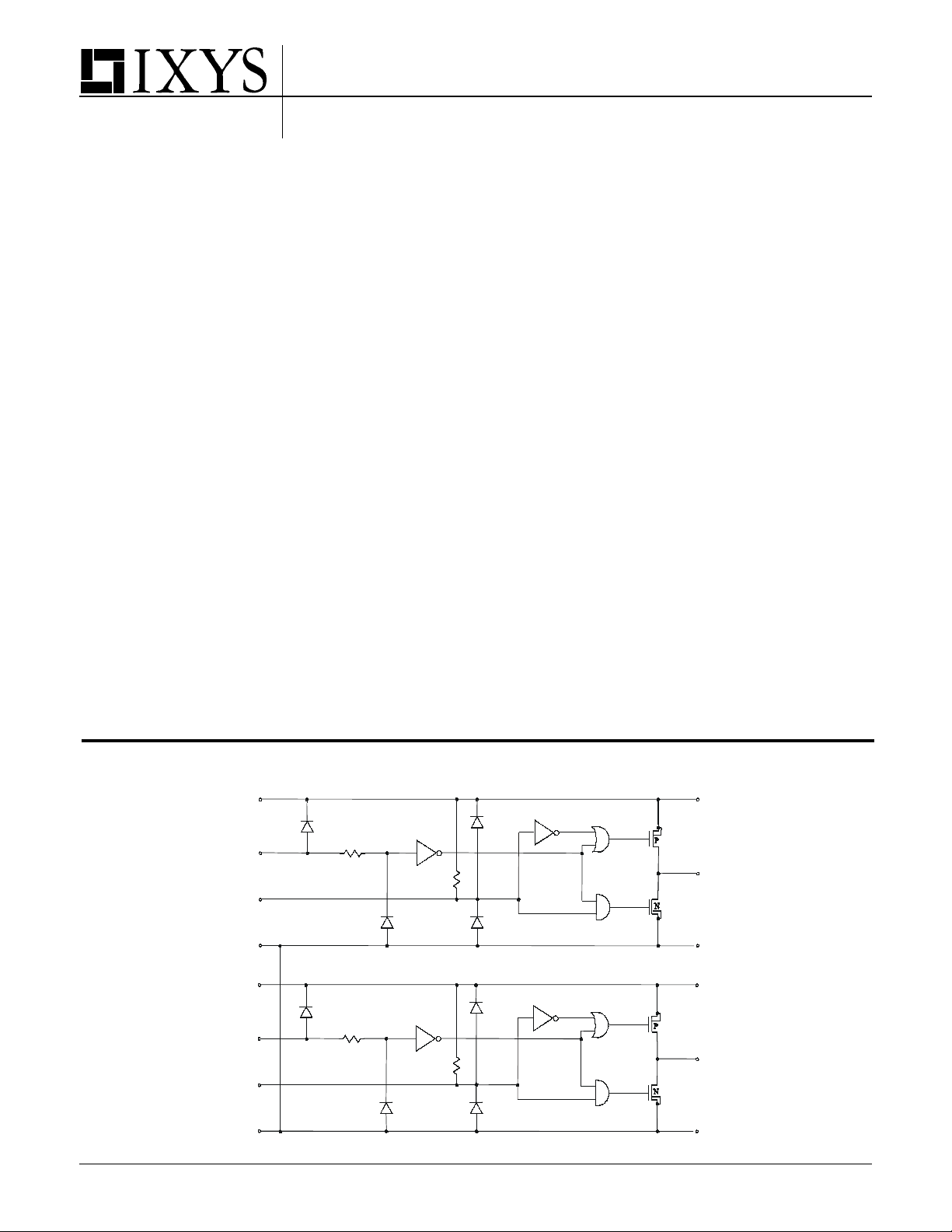
Figure 1 - Functional Diagram
Vcc (1, 2)
INA (7)
ENA (6)
GND (25, 26)
Vcc (11, 12)
INB (8)
ENB (9)
The IXDD415 is available in a 28 pin SO package (IXDD415SI),
incorporating DEI's patented
(1)
RF layout techniques to minimize
stray lead inductances for optimum switching performance.
(1)
DEI U.S. Patent #4,891,686
Vcc (3, 4)
200k
200k
OUTA (22, 23, 24)
GND (27, 28)
Vcc (13, 14)
OUTB (19, 20, 21)
GND (15, 16)
Copyright © IXYS CORPORATION 2001 Patent Pending
GND (17, 18)
First Release
Page 2
IXDD415SI
Absolute Maximum Ratings
Parameter Value
Supply Voltage 30V
All Other Pins -0.3V to VCC + 0.3V
Power Dissipation
T
T
AMBIENT
≤25 oC
CASE
≤25 oC
(Note 1) Operating Ratings
Parameter Value
Maximum Junction Temperature
Operating Temperature Range
1W
12W
Thermal Impedance (Junction To Case)
28 Pin SOIC (SI) (θJC)
150oC
-40oC to 85oC
0.75oC/W
Derating Factors (to Ambient)
28-Pin SOIC
Storage Temperature
Soldering Lead Temperature
(10 seconds maximum)
0.1W/oC
-65oC to 150oC
300oC
Electrical Characteristics
Unless otherwise noted, TA = 25 oC, 4.5V ≤ V
All voltage measurements with respect to GND. IXDD415 configured as described in Test Conditions.
Symbol Parameter Test Conditions Min Typ Max Units
V
IH
High input voltage 3.5 V
VIL Low input voltage 0.8 V
VIN Input voltage range -5 V
IIN Input current
VOH High output voltage V
VOL Low output voltage 0.025 V
ROH Output resistance
@ Outp u t High
ROL Output resistance
@ Outp u t L o w
I
Peak output current VCC = 15V, each output
PEAK
I
Continuous output
DC
curre nt
V
EN
V
High En input voltage 2/3 Vcc V
ENH
V
Low En input voltage 1/3 Vcc V
ENL
f
Maximum frequency CL=1.0nF Vcc=15V, max CW frequency
MAX
tR Rise time
tF Fall time
t
ONDLY
t
OFFDLY
P
Minimum pulse width FWHM CL=1nF
Wmin
t
Enable to output low
ENOL
Enable voltage range -0.3 Vcc + 0.3 V
(1)
C
(1)
C
On-time propagation
Off-time propagation
delay
delay
(1)
(1)
delay time
t
Enable to output high
ENOH
delay time
t
Disable to output low
DOLD
Disable delay time
t
Disable to output high
DOHD
Disable delay time
VCC Power supply voltage 8 15 30 V
ICC Power supply current V
(1)
Refer to Figures 2a and 2b
Specifications Subject To Change Without Notice
≤ 25V .
CC
+ 0.3 V
CC
0V ≤ V
I
= 10mA , V
OUT
I
= 10mA , V
OUT
IN
≤ V
CC
= 15V
CC
= 15V 0.8 1.2
CC
-10 10
- 0.025 V
CC
0.8 1.2
µA
Ω
Ω
15 A
2 A
45 MHz
limit e d by pac kag e p ow e r diss ip a t io n
=1nF Vcc=15V VOH=2 V to 12 V
L
=4nF Vcc=15V VOH=2 V to 12 V
C
L
=1nF Vcc=15V VOH=2 V to 12 V
L
=4nF Vcc=15V VOH=2 V to 12 V
C
L
C
=4nF Vcc=15V 32 38 ns
L
C
=4nF Vcc=15V 29 35 ns
L
2.5
4.5
2.0
3.5
5.0
+3V to +3V C
=1nF
L
7.0
ns
ns
ns
ns
ns
ns
Vcc=15V 80 ns
Vcc=15V 170 ns
Vcc=15V 30 ns
Vcc=15V 30 ns
IN
V
IN
V
IN
= 3.5V
= 0V
= + VCC
1 0 3
10
10
mA
µA
µ
A
2
Page 3
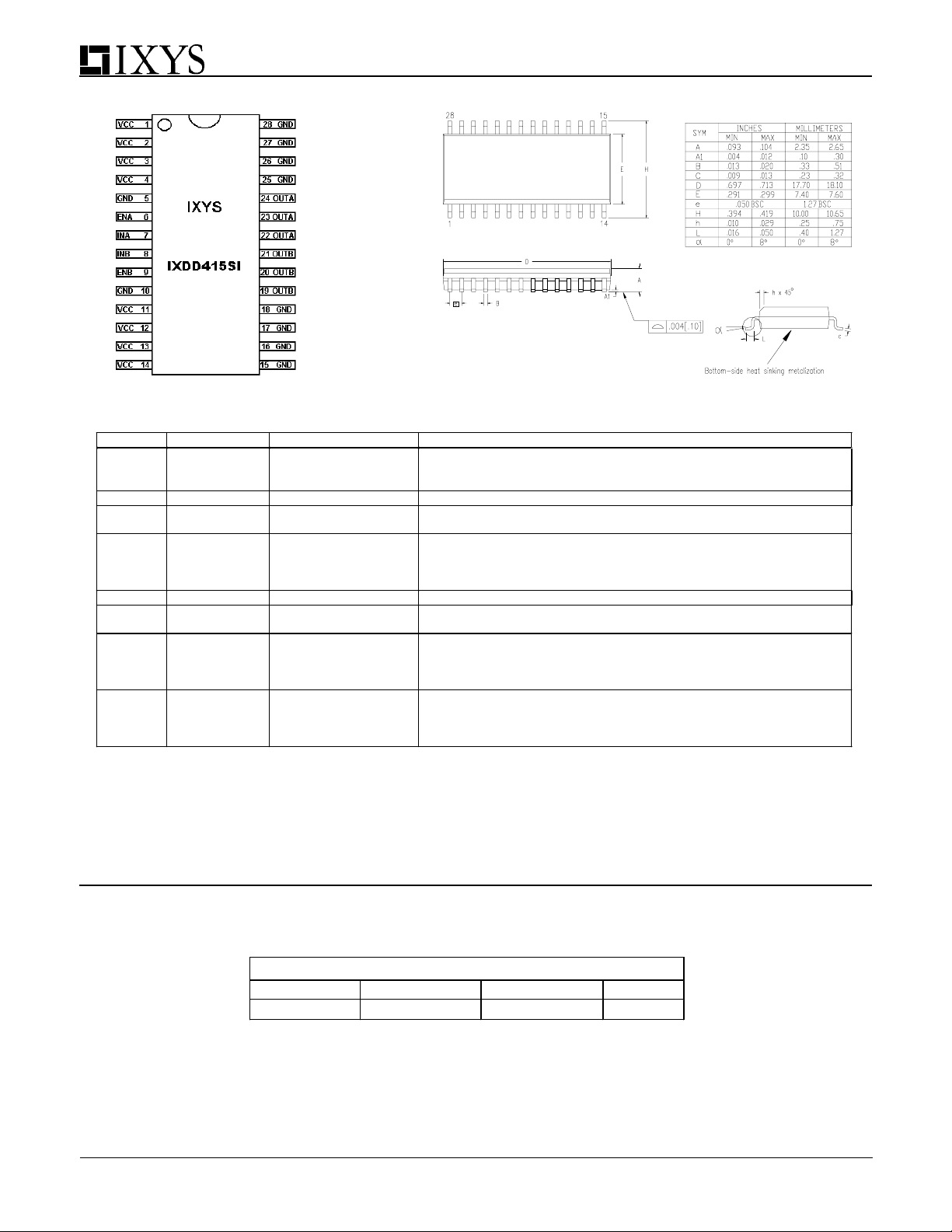
Pin Configurations And Package Outline
NOTE: Bottom-side heat sinking metalization is connected to ground
Pin Description
PIN # SYMBOL FUNCTION DESCRIPTION
1-4
11-14
7 INA Input Input signal-TT L or CM O S com patible.
6 ENA Enable
22-24 OUTA
8 INB Input Input signal-TT L or CM O S com patible.
9 ENB Enable
19-21 OUTB Output
5,10
15-18
25-28
VCC Supply Voltage
Output
GND Ground
Positive power-supply voltage input. This pin provides power
to the entire chip. The range for this voltage is from 8V to
30V.
The system enable pin. This pin, when driven low, disables
the chip, forcing high impedance state to the output.
Driver Output. For application purposes, this pin is
connected to the Gate of a MOS FET. In some app lications,
a low-impedance series resistor may be required between
this o u tp u t a nd the M OSFET Gate .
The system enable pin. This pin, when driven low, disables
the chip, forcing high impedance state to the output.
Driver Output. For application purposes, this pin is
connected to the Gate of a MOS FET. In some app lications,
a low-impedance series resistor may be required between
this o u tp u t a nd the M OSFET Gate .
The system ground pins. Internally connected to all circuitry,
these pins provide ground reference for the entire chip. All of
these pins should be connected to a low noise analog
ground plane for optim um performance.
IXDD415SI
Note 1: Operating the device beyond parameters with listed “Absolute Maximum Ratings” may cause permanent
damage to the device. Typical values indicate conditions for which the device is intended to be functional, but do not
guarantee specific performance limits. The guaranteed specifications apply only for the test conditions listed.
Exposure to absolute maximum rated conditions for extended periods may affect device reliability.
CAUTION: These devices are sensitive to electrostatic discharge; follow proper ESD procedures
when handling and assembling this component.
Ordering Information
Part Number Package Type Temp. Range Grade
IXDD415SI 28-Pin SOIC
-40°C to +85°C
3
Industrial
Page 4
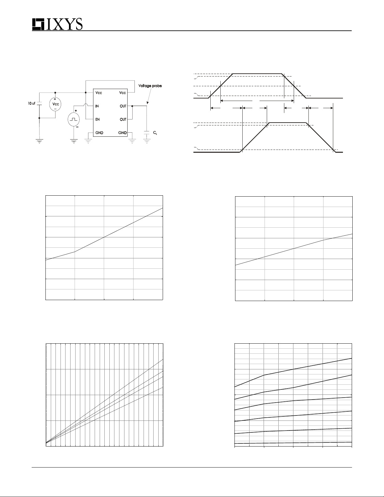
Typical Performance Characteristics
IXDD415SI
Figure 2a - Characteristics Test Diagram
V
IN
Fig. 3
5
4
3
Rise Time vs. Load Capacitance
= 15V, VOH = 2V To 12V
V
CC
Figure 2b - Timing Diagram
5V
90%
INPUT
2.5V
10%
0V
t
ONDLY
Vcc
90%
OUTPUT
10%
0V
Fig. 4
PW
MIN
OFFDLY
t
R
t
t
F
Fall Time vs. Load Capacitance
= 15V, VOH = 12V T o 2V
V
CC
5
4
3
Rise Time (ns)
Fig. 5
4000
3000
2000
Supply Current (mA )
1000
2
2
Fall Time (ns)
1
0
1k 2k 3k 4k0
Load Capa citance (pF)
Supply Current vs. Frequency
Vcc=15V
4 nF
2 nF
1 nF
= 0
C
L
Fig. 6
4000
3000
2000
Supply Current (mA )
1000
1
0
1k 2k 3k 4k0
Load Capa citance (pF)
Supply Current vs. Load Capacitance
Vcc=15V
25 MHz
20 MHz
15 MHz
10 MHz
5 MHz
1 MHz
0
5 10152025
Frequency (MHz)
0
0k 1k 2k 3k 4k
Load Capa citance (pF)
4
Page 5
IXDD415SI
)
Fig. 7
50
40
30
20
Propagation Delay (ns)
10
0
8 1012141618
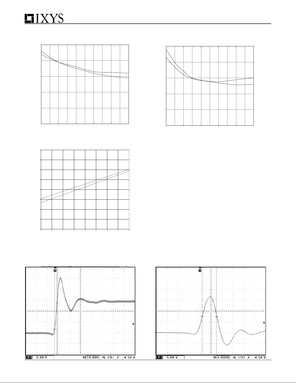
Propagation Delay vs. Supply Voltage
=4nF VIN=5V@ 100kH z
C
L
t
ONDLY
t
OFFDLY
Supply Voltage (V)
Fig. 9
50
45
40
Propagation Delay vs. Junction Temperature
=4nF, VCC=15V
C
L
t
ONDLY
Fig. 8
50
40
30
20
Propagation Delay (ns)
10
0
24681012
Propagation Delay vs. Input Voltage
=4nF VCC=15V
C
L
t
ONDLY
t
OFFDLY
Input Voltage (V)
35
30
Time (ns)
25
20
15
10
-40-200 20406080100120
t
OFFDLY
Temperature (°C
Typical Output Waveforms
Unless otherwise noted, all waveforms are taken driving a 1nF load, 1MHz repetition frequency, VCC=15V, Case Temperature = 25°C
Figure 10 2.2ns Rise Time
Figure 11 <6ns Minimum Pulse Width
5
Page 6
IXDD415SI
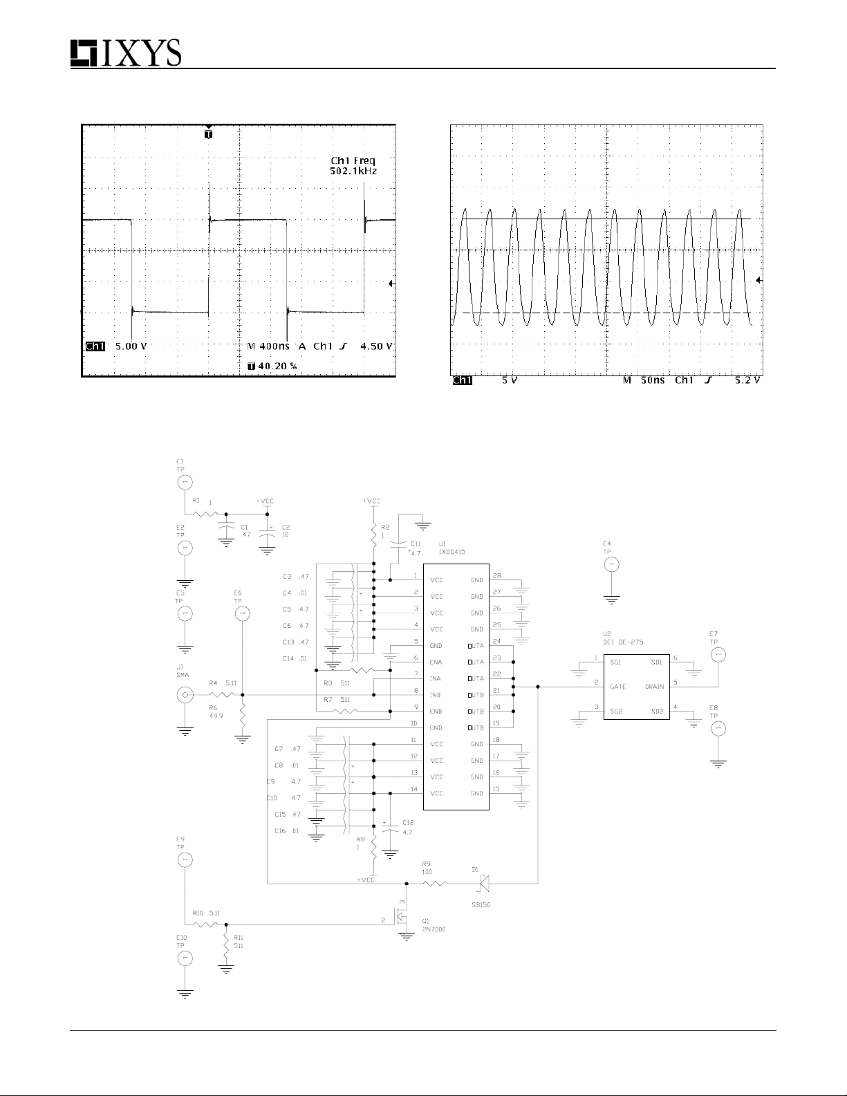
Figure 12 500KHz CW Repetition Frequency
Figure 14 - High Frequency Gate Drive Circuit
Figure 13 50MHz Burst Repetition Frequency
6
Page 7
APPLICATIONS INFORMATION
High Frequency Gate Drive Circuit
IXDD415SI
The circuit diagram in figure 14 is a circuit diagram for a
very high switching speed, high frequency gate driver
circuit using the IXDD415SI. This is the circuit used in
the EVDD415 Evaluation Board,and is capable of driving
a MOSFET at up to the maximum operating limits of the
IXDD415. The circuit's very high switching speed and
high frequency operation dictates the close attention to
several important issues with respect to circuit design.
The three key elements are circuit loop inductance, Vcc
bypassing and grounding.
Circuit Loop Inductance
Referring to Figure 14, the Vcc to Vcc ground current
path defines the loop which will generate the inductive
term. This loop must be kept as short as possible. The
output leads (pins 24, 23, 22, 21, 20, and 19) must be
no further than 0.375 inches (9.5mm) from the gate of
the MOSFET. Furthermore the output ground leads (pins
25, 26, 27 and 28 on one end of the IC and pins 15, 16,
17, and 18 on the other end of the IC) must provide a
balanced symmetric coplanar ground return for optimum
operation.
Vcc Bypassing
In order for the circuit to turn the MOSFET on properly,
the IXDD415 must be able to draw up to 15A of current
per output channel from the Vcc power supply in 2-6ns
(depending upon the input capacitance of the MOSFET
being driven). This means that there must be very low
impedance between the driver and the power supply.
The most common method of achieving this low
impedance is to bypass the power supply at the driver
with a capacitance value that is at least two orders of
magnitude larger than the load capacitance. Usually,
this is achieved by placing two or three different types of
bypassing capacitors, with complementary impedance
curves, very close to the driver itself. (These capacitors
should be carefully selected, low inductance, low
resistance, high-pulse current-service capacitors). Care
should be taken to keep the lengths of the leads
between these bypass capacitors and the IXDD415 to an
absolute minimum.
returning current that need to be considered: Path #1 is
between the IXDD415 and its load. Path #2 is between the
IXDD415 and its power supply. Path #3 is between the
IXDD415 and whatever logic is driving it. All three of these
paths should be as low in resistance and inductance as
possible, and thus as short as practical.
Output Lead Inductance
Of equal importance to supply bypassing and grounding are
issues related to the output lead inductance. Every effort
should be made to keep the leads between the driver and
its load as short and wide as possible, and treated as
coplanar transmission lines.
In configurations where the optimum configuration of circuit
layout and bypassing cannot be used, a series resistance
of a few Ohms in the gate lead may be necessary to prevent
ringing.
Heat Sinking
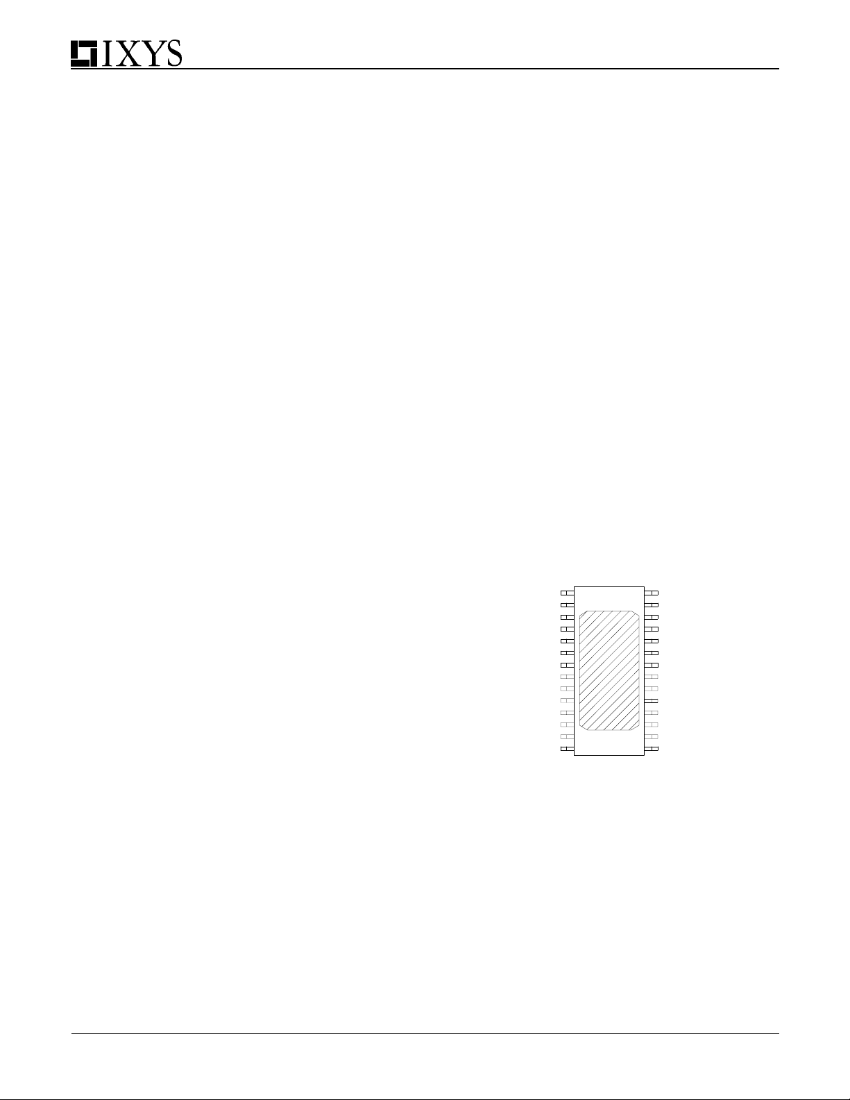
For high power operation, the bottom side metalized heat
sink pad should be epoxied to the circuit board ground
plane, or attached to an appropriate heat sink, using
thermally conductive epoxy. The heat sink tab is connected
to ground.
Figure 15: IXDD415SI Bottom Side
Heat Sinking Metalization
The bypassing should be comprised of several values of
chip capacitors symmetrically placed on ether side of
the IC. Recommended values are .01uF, .47uF chips
and at least two 4.7uF tantalums.
Grounding
In order for the design to turn the load off properly, the
IXDD415 must be able to drain this 15A of current into an
adequate grounding system. There are three paths for
7
Page 8
TTL to High Voltage CMOS Level Translation
ge
IXDD415SI
The enable (EN) input to the IXDD415 is a high voltage
CMOS logic level input where the EN input threshold is ½ V
and may not be compatible with 5V CMOS or TTL input levels.
CC
The IXDD415 EN input was intentionally designed for
enhanced noise immunity with the high voltage CMOS logic
levels. In a typical gate driver application, V
EN input threshold at 7.5V, a 5V CMOS logical high input
=15V and the
CC
applied to this typical IXDD415 application’s EN input will be
misinterpreted as a logical low, and may cause undesirable
or unexpected results. The note below is for optional
adaptation of TTL or 5V CMOS levels.
The circuit in Figure 16 alleviates this potential logic level
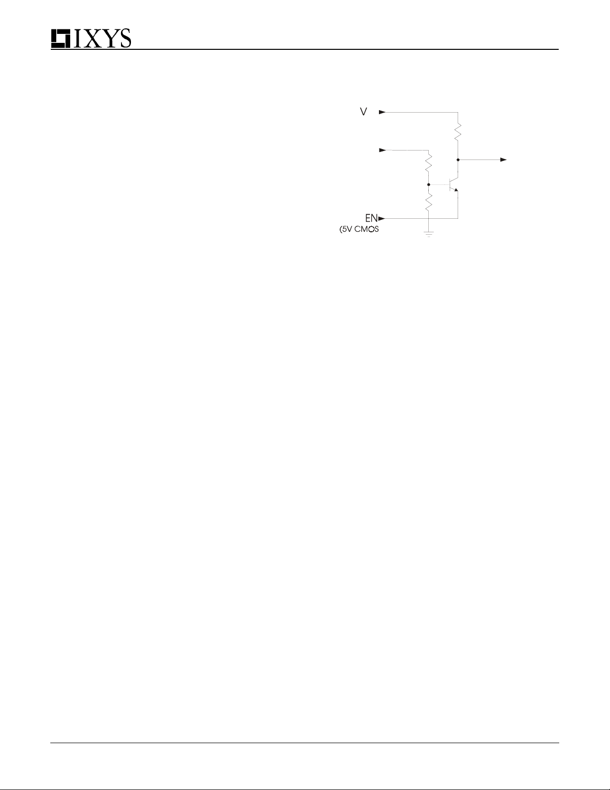
misinterpretation by translating a TTL or 5V CMOS logic input
to high voltage CMOS logic levels needed by the IXDD415 EN
input. From the figure, VCC is the gate driver power supply,
typically set between 8V to 20V, and VDD is the logic power
supply, typically between 3.3V to 5.5V. Resistors R1 and R2
form a voltage divider network so that the Q1 base is positioned at the midpoint of the expected TTL logic transition
levels.
A TTL or 5V CMOS logic low, V
the Q1 emitter will drive it on. This causes the level translator
output, the Q1 collector output to settle to V
V
=<~2V, which is sufficiently low to be correctly
TTLLOW
interpreted as a high voltage CMOS logic low (<1/3VCC=5V for
=~<0.8V, input applied to
TTLLOW
CESATQ1
+
VCC =15V given in the IXDD415 data sheet.)
Figure 16 - TTL to High Voltage CMOS Level Translator
,
CC
(From G a te D river
Power Supply)
V
DD
(From Log ic
Power Supply)
or
TTL
Inpu t)
3.3K
3.3K R2
R1
10K
R3
Q1
2N3904
High V olta
CMOS
Output
(To IXDD415
EN Input)
EN
A TTL high, V
V
5VCMOSHIGH
Figure 16 will cause Q1 to be biased off. This results in Q1
=~>3.5V, applied to the EN input of the circuit in
=>~2.4V, or a 5V CMOS high,
TTLHIGH
collector being pulled up by R3 to VCC=15V, and provides a
high voltage CMOS logic high output. The high voltage CMOS
logical EN output applied to the IXDD415 EN input will enable
it, allowing the gate driver to fully function as a 15 Ampere
output driver.
The total component cost of the circuit in Figure 16 is less
than $0.10 if purchased in quantities >1K pieces. It is
recommended that the physical placement of the level
translator circuit be placed close to the source of the TTL or
CMOS logic circuits to maximize noise rejection.
Directed Energy, Inc.
An IXYS Company
2401 Research Blvd. Ste. 108, Ft. Collins, CO 80526
Tel: 970-493-1901; Fax: 970-493-1903
e-mail: [email protected]
www.directedenergy.com
IXYS Corporation
3540 Bassett St; Santa Clara, CA 95054
Tel: 408-982-0700; Fax: 408-496-0670
e-mail: [email protected]
www.ixys.com
IXYS Semiconductor GmbH
Edisonstrasse15 ; D-68623; Lampertheim
Tel: +49-6206-503-0; Fax: +49-6206-503627
e-mail: [email protected]
8
Doc #9200-0233 R2
 Loading...