

Page 1
IXDD408PI / 408SI / 408YI / 408CI
8 Amp Low-Side Ultrafast MOSFET Driver
Features
• Built using the advantages and compatibility
of CMOS and IXYS HDMOSTM processes.
• Latch Up Protected
• High Peak Output Current: 8A Peak
• Operates from 4.5V to 25V
• Ability to Disable Output under Faults
• High Capacitive Load
Drive Capability: 2500pF in <15ns
• Matched Rise And Fall Times
• Low Propagation Delay Time
• Low Output Impedance
• Low Supply Current
Applications
• Driving MOSFETs and IGBTs
• Limiting di/dt under Short Circuit
• Motor Controls
• Line Drivers
• Pulse Generators
• Local Power ON/OFF Switch
• Switch Mode Power Supplies (SMPS)
• DC to DC Converters
• Pulse Transformer Driver
• Class D Switching Amplifiers
General Description
The IXDD408 is a high speed high current gate driver
specifically designed to drive the largest MOSFETs and
IGBTs to their minimum switching time and maximum
practical frequency limits. The IXDD480 can source and
sink 8A of peak current while producing voltage rise and
fall times of less than 30ns. The input of the driver is
compatible with TTL or CMOS and is fully immune to
latch up over the entire operating range. Designed with
small internal delays, cross conduction/current shootthrough is virtually eliminated in the IXDD408. Its features
and wide safety margin in operating voltage and power
make the IXDD408 unmatched in performance and value.
The IXDD408 incorporates a unique ability to disable the
output under fault conditions. When a logical low is
forced into the Enable input, both final output stage
MOSFETs (NMOS and PMOS) are turned off. As a
result, the output of the IXDD408 enters a tristate mode
and achieves a Soft Turn-Off of the MOSFET/IGBT when
a short circuit is detected. This helps prevent damage
that could occur to the MOSFET/IGBT if it were to be
switched off abruptly due to a dv/dt over-voltage transient.
The IXDD408 is available in the standard 8-pin P-DIP (PI),
SOP-8 (SI), 5-pin TO-220 (CI) and in the TO-263 (YI)
surface-mount package.
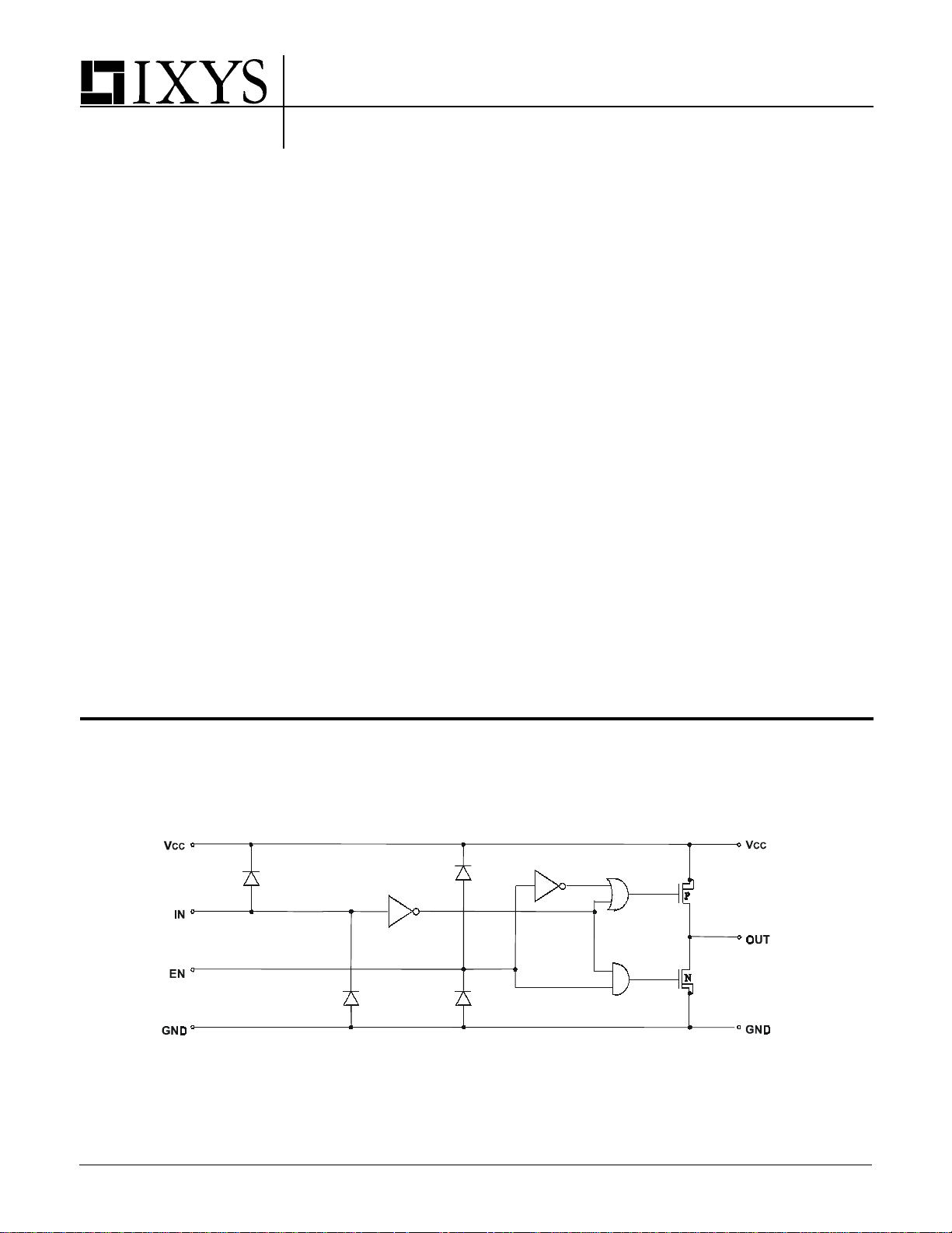
Figure 1 - Functional Diagram
Copyright © IXYS CORPORATION 2001 Patent Pending
First Release
Page 2
IXDD408PI/408SI//408YI/408CI
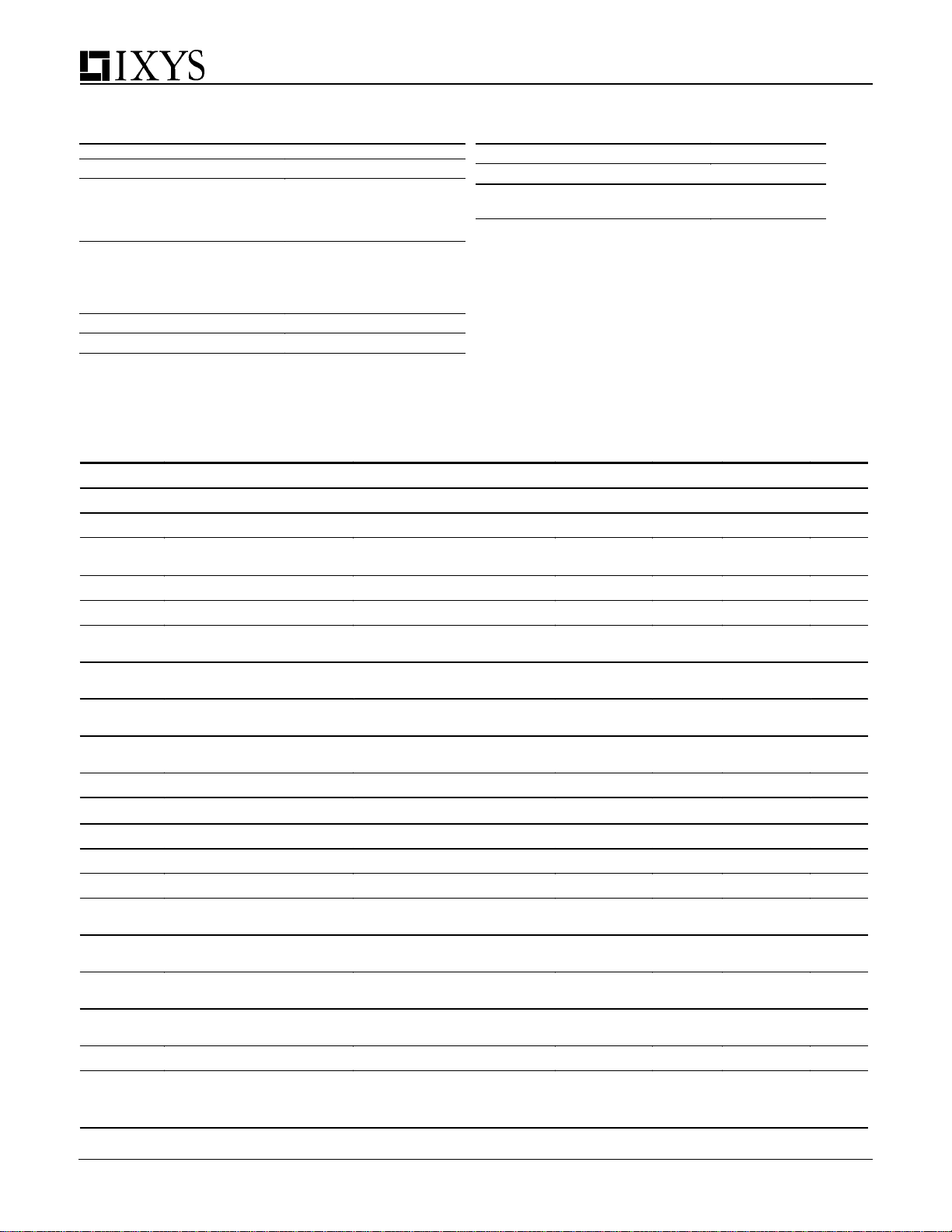
Absolute Maximum Ratings (Note 1)
Parameter Value
Supply Voltage 25 V
All Other Pins -0.3 V to VCC + 0.3 V
Power Dissipation, T
8 Pin PDIP (PI) 975mW
8 Pin SOIC (SI) 1055mW
TO220 (CI), TO263 (YI) 17W
Derating Factors (to Ambient)
8 Pin PDIP (PI)
8 Pin SOIC (SI)
TO220 (CI), TO263 (YI)
Storage Temperature
Lead Temperature (10 sec)
AMBIENT
≤25 oC
7.6mW/oC
8.2mW/oC
0.14W/oC
-65 oC to 150 oC
300 oC
Operating Ratings
Parameter Value
Maximum Junction Temperature
Operating Temperature Range
Thermal Impedance (Junction To Case)
TO220 (CI), TO263 (YI) (θJC)
150 oC
-40 oC to 85 oC
0.95 oC/W
Electrical Characteristics
Unless otherwise noted, TA = 25 oC, 4.5V ≤ V
All voltage measurements with respect to GND. IXDD408 configured as described in Test Conditions.
Symbol Parameter Test Conditions Min Typ Max Units
V
IH
High input voltage 3.5 V
VIL Low input voltage 0.8 V
VIN Input voltage range -5 V
IIN Input current
VOH High output voltage V
VOL Low output voltage 0.025 V
ROH Output resistance
@ Output high
ROL Output resistance
@ Output Low
I
Peak output current VCC is 18V
PEAK
I
Continuous output
DC
current
V
EN
V
High En Input Voltage 2/3 Vcc V
ENH
V
Low En Input Voltage 1/3 Vcc V
ENL
Enable voltage range - .3 Vcc + 0.3 V
tR Rise time CL=2500pF Vcc=18V 12 14 18 ns
tF Fall time CL=2500pF Vcc=18V 13 15 19 ns
t
On-time propagation
ONDLY
delay
t
Off-time propagation
OFFDLY
delay
t
Enable to output high
ENOH
delay time
t
Disable to output low
DOLD
Disable delay time
VCC Power supply voltage 4.5 18 25 V
ICC Power supply current V
Specifications Subject To Change Without Notice
≤ 25V .
CC
+ 0.3 V
CC
0V ≤ V
IN
≤
V
CC
-10 10
µ
A
- 0.025 V
CC
I
= 10mA, V
OUT
CC
= 18V
0.8 1.5
Ω
I
= 10mA, V
OUT
= 18V 0.8 1.5
CC
Ω
8 A
Limited by package power
2 A
dissipation
CL=2500pF Vcc=18V 37 38 42 ns
CL=2500pF Vcc=18V 32 34 38 ns
Vcc=18V 52 ns
Vcc=18V 30 ns
IN
V
IN
V
IN
= 3.5V
= 0V
= + VCC
1 0 3
10
10
mA
µ
A
µ
A
2
Page 3
Pin Configurations
1
2
3
4
VCC
IN
EN
GND
IXDD408PI/408SI/408YI/408CI
IXDD408CI
VCC
GND
8
7
6
5
1
2
3
4
5
Vcc
OUT
GND
IN
EN
I
X
OUT
D
D
OUT
4
0
8
IXDD408YI
8 PIN DIP (PI)
SO8 (SI)
TO220 (CI)
TO263 (YI)
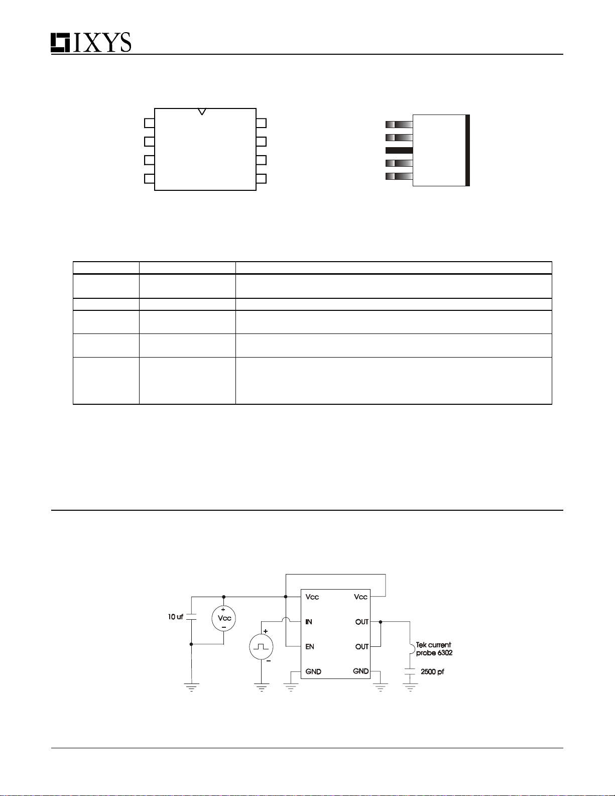
Pin Description
SYMBOL FUNCTION DESCRIPTION
VCC Supply Voltage
Positiv e power-supply v oltage input. This pin provides power to the
entire chip. T he r ange f or this voltage is from 4.5V to 25V.
IN Input Input si gnal-TTL or CMOS compatible.
EN Enable
OUT Output
The system enabl e pin. This pi n, when driven low, di sables the chi p,
forcing high im pedance stat e to the output.
Driver Output. For application purposes, this pin is connected,
through a resistor, to Gate of a MOSFET/IGBT.
The system ground pin. Inter nally connected t o all circuit ry, this pin
GND Ground
provides ground reference for the entire chip. This pin should be
connected to a low noise analog ground plane for optimum
performance.
Note 1: Operating the device beyond parameters with listed “absolute maximum ratings” may cause permanent
damage to the device. Typical values indicate conditions for which the device is intended to be functional, but do not
guarantee specific performance limits. The guaranteed specifications apply only for the test conditions listed.
Exposure to absolute maximum rated conditions for extended periods may affect device reliability.
CAUTION: These devices are sensitive to electrostatic discharge; follow proper ESD procedures
when handling and assembling this component.
Figure 2 - Characteristics Test Diagram
IN
V
3
Page 4
IXDD408PI/408SI//408YI/408CI
)
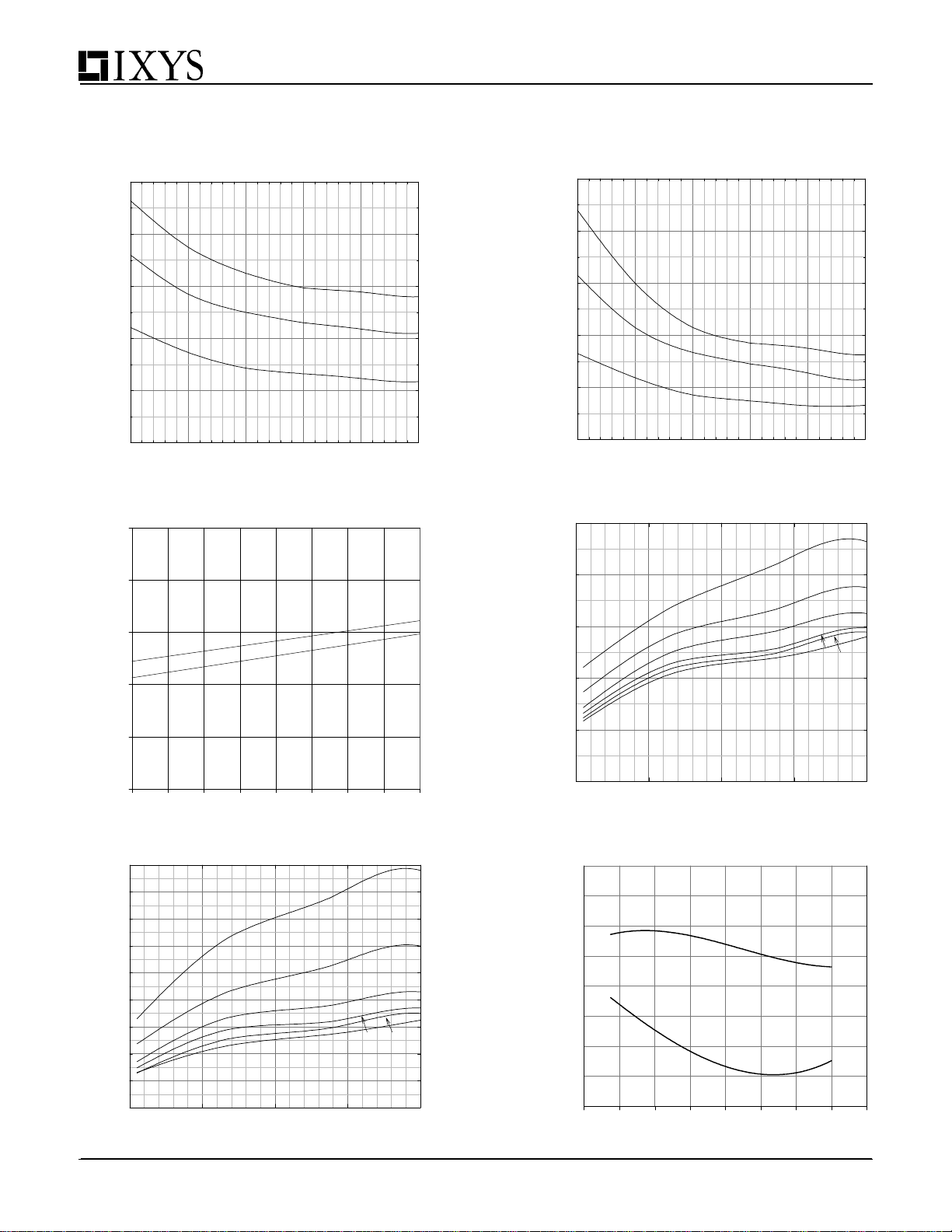
Typical Performance Characteristics
Fig. 3
50
40
30
20
Rise Time (ns)
10
0
8 1012141618
Rise Time vs. Supply Voltage
CL=10,000 pF
4700 pF
2200 pF
S u p p ly Volta g e (V)
Fig. 5
Rise And Fall Times vs. Junction Temperature
= 2500pF, VCC = 18V
C
25
20
15
t
F
10
Time (ns)
t
R
L
Fig. 4
100
80
60
40
Fall Time (ns)
20
0
81012141618
Fall Tim e vs. Supply Voltage
CL=10,000 pF
4700 pF
2200 pF
Supply Voltage (V)
Fig. 6
50
40
30
20
Rise Time vs. Load Capacitance
14V
16V
8V
10V
12V
18V
Rise Time (ns)
5
0
-40 -20 0 20 40 60 80 100 120
Temperature (°C
Fig. 7
90
80
70
60
50
40
Fall Time (ns)
30
20
10
0
2k 4k 6k 8k 10k
Fall Time vs. Load Capacitance
14V
Load Capacitance (pF)
16V
10V
12V
10
0
2k 4k 6k 8k 10k
Load Capa citance (pF)
Fig. 8
8V
18V
3.2
3.0
2.8
2.6
2.4
2.2
Max / Min Input (V)
2.0
1.8
1.6
Max / Min Input vs. Junction Temperature
C
=2500pF VCC = 18V
L
Minimum Input High
Maximum Input Low
-60 -40 -20 0 20 40 60 80 100
Tempe rature (oC)
4
Page 5
IXDD408PI/408SI/408YI/408CI
)
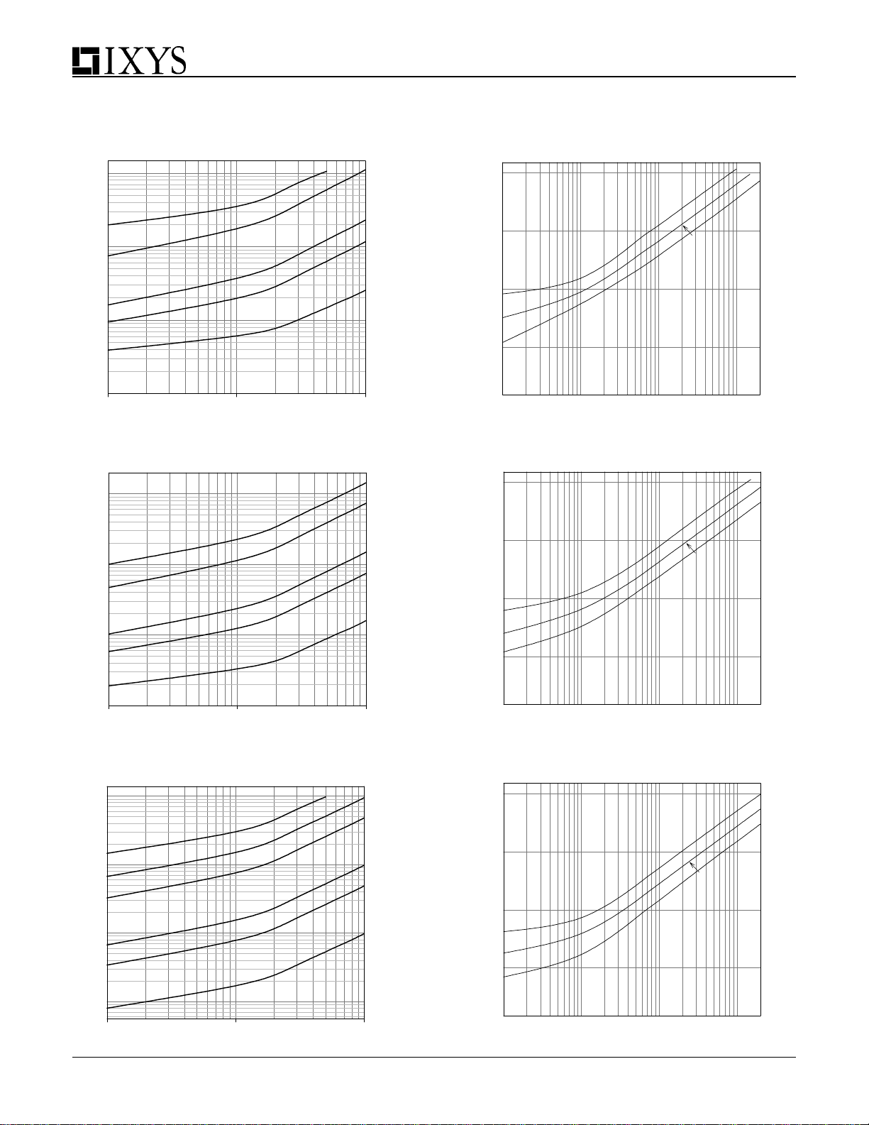
Fig. 9 Fig. 10
Supply Current vs. Load Capacitance
Vcc=18V
100
1 MHz
10
500 KHz
100 kHz
1
50 kHz
Supply Current (mA)
10 kHz
0.1
0.1k 1.0k 10.0k
Load Capa citance (pF)
Fig. 11
Supply Current vs. Load Capacitance
100
10
1
S up p ly C u rre n t (m A)
0.1
1 10 100 1000
Fig. 12
Vcc=12V
100
10
1 MHz
500 KHz
100
10
1
Supply Current vs. Frequency
Vcc=18V
CL= 5000 pF
2500 pF
1000 pF
Frequency (kHz)
Supply Current vs. Frequency
Vcc=12V
CL= 5000 pF
2500 pF
1000 pF
1
100 kHz
Supply Current (mA)
50 kHz
10 kHz
0.1
0.1k 1.0k 10.0k
Load Capacitance (pF)
Fig. 13
Supply Current vs. Load Capacitance
Vcc=8V
100
2 MHz
10
1 MHz
500 KHz
1
100 kHz
Supply Current (mA)
50 kHz
0.1
10 kHz
0.1k 1.0k 10.0k
Load Capacitance (pF
Supply Current (mA)
0.1
1 10 100 1000
Frequency (kHz)
Fig. 14
Supply Current vs. Frequency
Vcc=8V
100
CL= 5000 pF
10
2500 pF
1
S up p ly C u rre n t (m A)
0.1
1 10 100 1000
Frequency (kHz)
1000 pF
5
Page 6
IXDD408PI/408SI//408YI/408CI
(
)
(
)
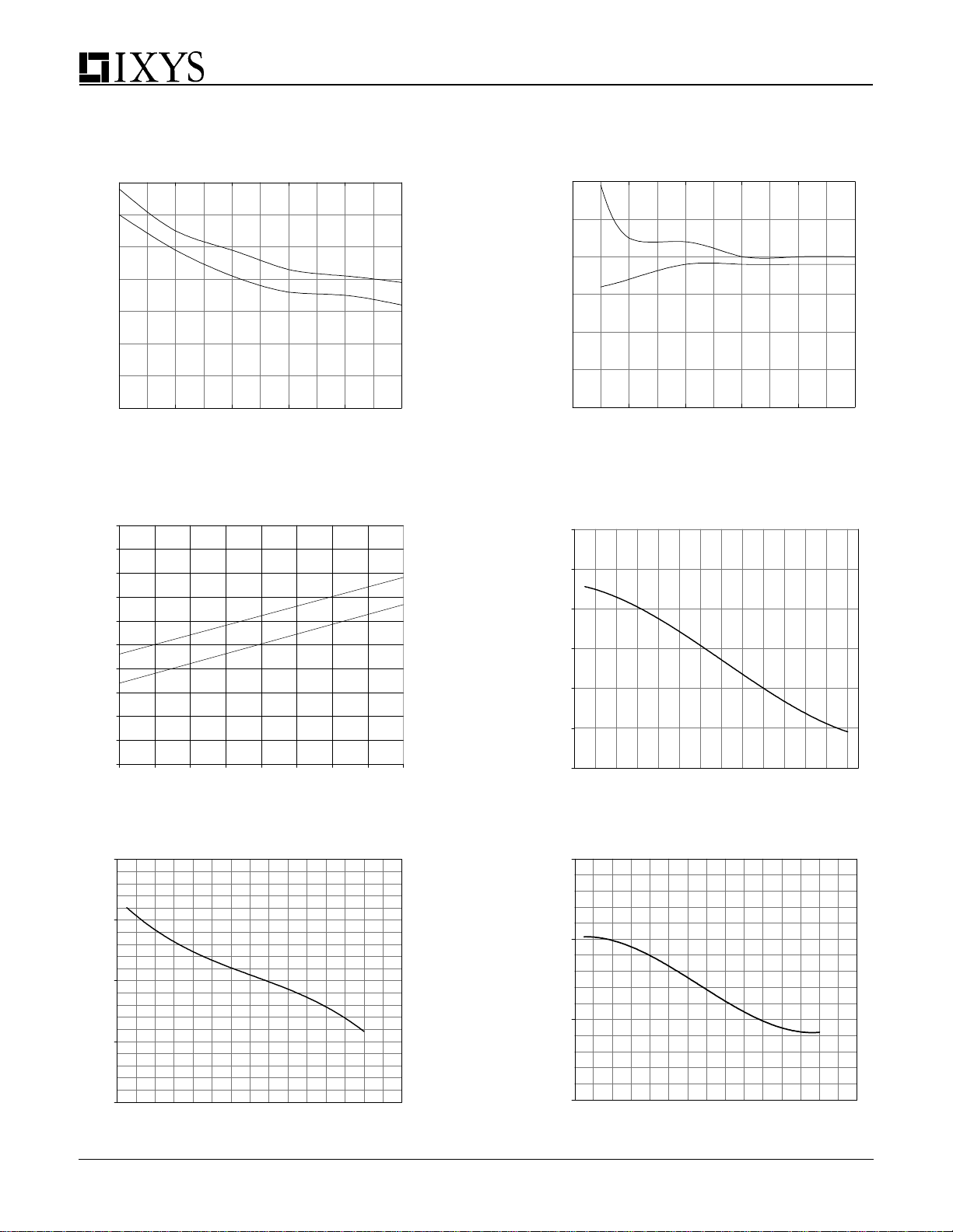
Fig. 15
70
60
50
40
30
20
Propagation Delay vs. Supply Voltage
=2500pF VIN=5V@1kHz
C
L
Propagation Delay (ns)
10
0
8 1012141618
Supply Voltage (V)
Fig. 17
Fig. 19
Propagation Delay Times vs. Junction Temperature
= 2500pF VCC = 18V
C
60
55
50
45
40
35
30
Time (ns)
25
20
15
10
-40-200 20406080100120
P Channel Peak Output Current vs. Case Temperature
12
L
Temperature
CI and YI Packages, C
°
C
=.1uF VCC=18V
L
t
ONDLY
t
OFFDLY
t
ONDLY
t
OFFDLY
Fig. 16
60
50
40
30
20
Propagation Delay vs. Input Voltage
=2500pF VCC=15V
C
L
t
ONDLY
t
OFFDLY
Propagation Delay (ns)
10
0
24681012
Input Voltage (V)
Fig. 18
Quiescent Supply Current (mA)
Quiescent Supply Current vs. Junction Temperature
=18V VIN=5V@1kHz
V
0.66
0.64
0.62
0.60
0.58
0.56
0.54
-40-200 20406080
Fig. 20
N Channel Peak Output Current vs. Case Temperature
9
CC
Temperature
CI and YI Packages, C
o
C
=.1uF VCC=18V
L
11
8
10
7
9
P Channel Output Current (A)
8
-40-200 20406080100
Temperature (oC)
N C hannel Output Current (A)
6
-40-200 20406080100
Temperature (oC)
6
Page 7
IXDD408PI/408SI/408YI/408CI
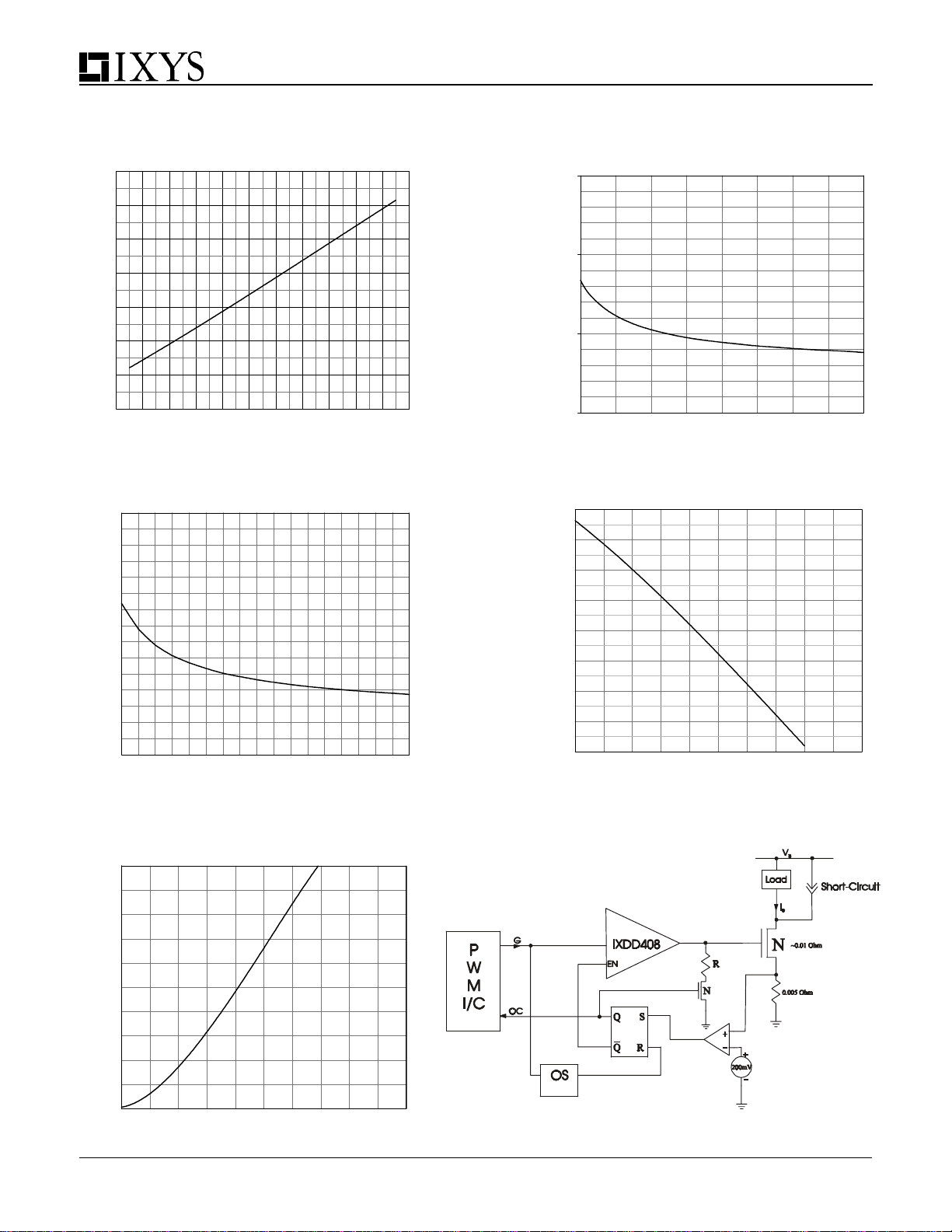
Fig. 21
14
12
10
Enable Threshold (V)
8
6
4
2
0
Enable Threshold vs. Supply Voltage
4 6 8 10 12 14 16 18 20 22 24 26
Supply Voltage (V)
Fig. 23
Low-State Output Resistance
vs. Supply Voltage
3.0
2.0
Fig. 22
3
2
1
High State Output Resistance
vs. Supply Voltage
High State Output Resistance (Ohm )
0
5 10152025
Supply Voltage (V)
Fig. 24
0
-2
-4
-6
Vcc vs. P Channel Output Current
=15nF
C
L
1.0
Low-State Output Resistance (Ohm s)
0.0
Fig. 25
N Channel Output Current (A)
8
10 15 20 25
Supply Voltage (V)
Vcc vs. N Channel Output Current
C
=15nF
10
8
6
4
2
L
-8
-10
-12
P Channel Output Current (A)
-14
-16
5 1015202530
Vcc
Figure 26 - Typical Application Short Circuit di/dt Limit
0
5 1015202530
Vcc
7
Page 8
APPLICATIONS INFORMATION
Short Circuit di/dt Limit
A short circuit in a high-power MOSFET module such as the
VM0580-02F, (580A, 200V), as shown in Figure 26, can cause
the current through the module to flow in excess of 1500A for
10µs or more prior to self-destruction due to thermal runaway.
For this reason, some protection circuitry is needed to turn off
the MOSFET module. However, if the module is switched off
too fast, there is a danger of voltage transients occuring on the
drain due to Ldi/dt, (where L represents total inductance in
series with drain). If these voltage transients exceed the
MOSFET's voltage rating, this can cause an avalanche breakdown.
The IXDD408 has the unique capability to softly switch off the
high-power MOSFET module, significantly reducing these
Ldi/dt transients.
Thus, the IXDD408 helps to prevent device destruction from
both dangers; over-current, and avalanche breakdown due to
di/dt induced over-voltage transients.
The IXDD408 is designed to not only provide ±8A under normal
conditions, but also to allow it's output to go into a high
impedance state. This permits the IXDD408 output to control
a separate weak pull-down circuit during detected overcurrent
shutdown conditions to limit and separately control d
turnoff. This circuit is shown in Figure 27.
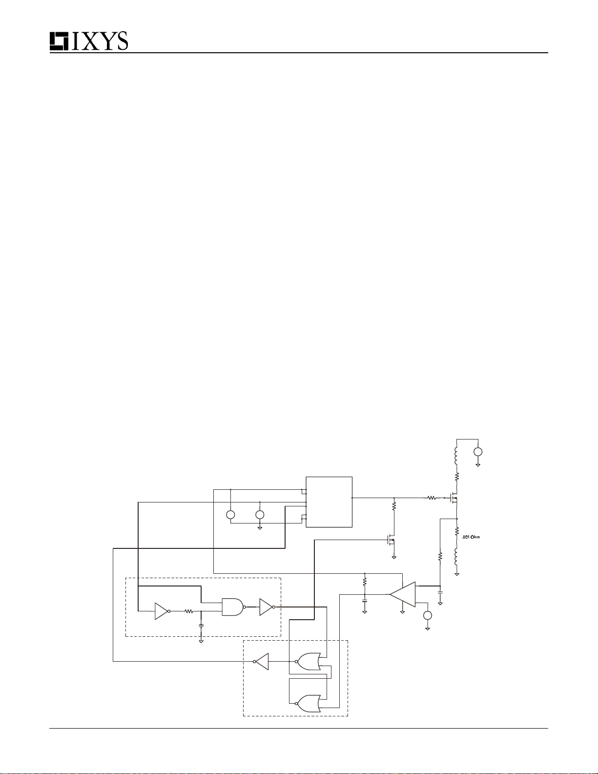
Referring to Figure 27, the protection circuitry should include
a comparator, whose positive input is connected to the source
of the VM0580-02. A low pass filter should be added to the input
of the comparator to eliminate any glitches in voltage caused
by the inductance of the wire connecting the source resistor to
VGS
/dt gate
IXDD408PI/408SI//408YI/408CI
ground. (Those glitches might cause false triggering of the
comparator).
The comparator's output should be connected to a SRFF(Set
Reset Flip Flop). The flip-flop controls both the Enable signal,
and the low power MOSFET gate. Please note that CMOS 4000series devices operate with a V
18 VDC being the maximum allowable limit).
A low power MOSFET, such as the 2N7000, in series with a
resistor, will enable the VMO580-02F gate voltage to drop
gradually. The resistor should be chosen so that the RC time
constant will be 100us, where "C" is the Miller capacitance of
the VMO580-02F.
For resuming normal operation, a Reset signal is needed at
the SRFF's input to enable the IXDD408 again. This Reset can
be generated by connecting a One Shot circuit between the
IXDD408 Input signal and the SRFF restart input. The One Shot
will create a pulse on the rise of the IXDD408 input, and this
pulse will reset the SRFF outputs to normal operation.
When a short circuit occurs, the voltage drop across the lowvalue, current-sensing resistor, (Rs=0.005 Ohm), connected
between the MOSFET Source and ground, increases. This
triggers the comparator at a preset level. The SRFF drives a low
input into the Enable pin disabling the IXDD408 output. The
SRFF also turns on the low power MOSFET, (2N7000).
In this way, the high-power MOSFET module is softly turned off
by the IXDD408, preventing its destruction.
range from 3 to 15 VDC, (with
CC
Figure 27 - Application Test Diagram
One Shot Circuit
NOT1
CD4049A
EN
Ros
1Mohm
Cos
1pF
+
-
NAND
CD4011A
VCC
SR Flip-Flop
+
VIN
-
NOT2
CD4049A
NOT3
CD4049A
Q
VCC
VCCA
IN
EN
GND
SUB
NOR1
CD4001A
NOR2
CD4001A
IXDD408
R
S
OUT
Rcomp
5kohm
Ccomp
+
Rd
0.1ohm
High_Power
VMO580-02F
Rs
Ls
20nH
0
VB
-
Ld
10uH
Rg
Low_Power
2N7002/PLP
V+
V-
1ohm
R+
10kohm
+
-
REF
C+
100pF
+
-
Rsh
1600ohm
Comp
LM339
1pF
8
Page 9
Supply Bypassing and Grounding Practices,
Output Lead inductance
IXDD408PI/408SI/408YI/408CI
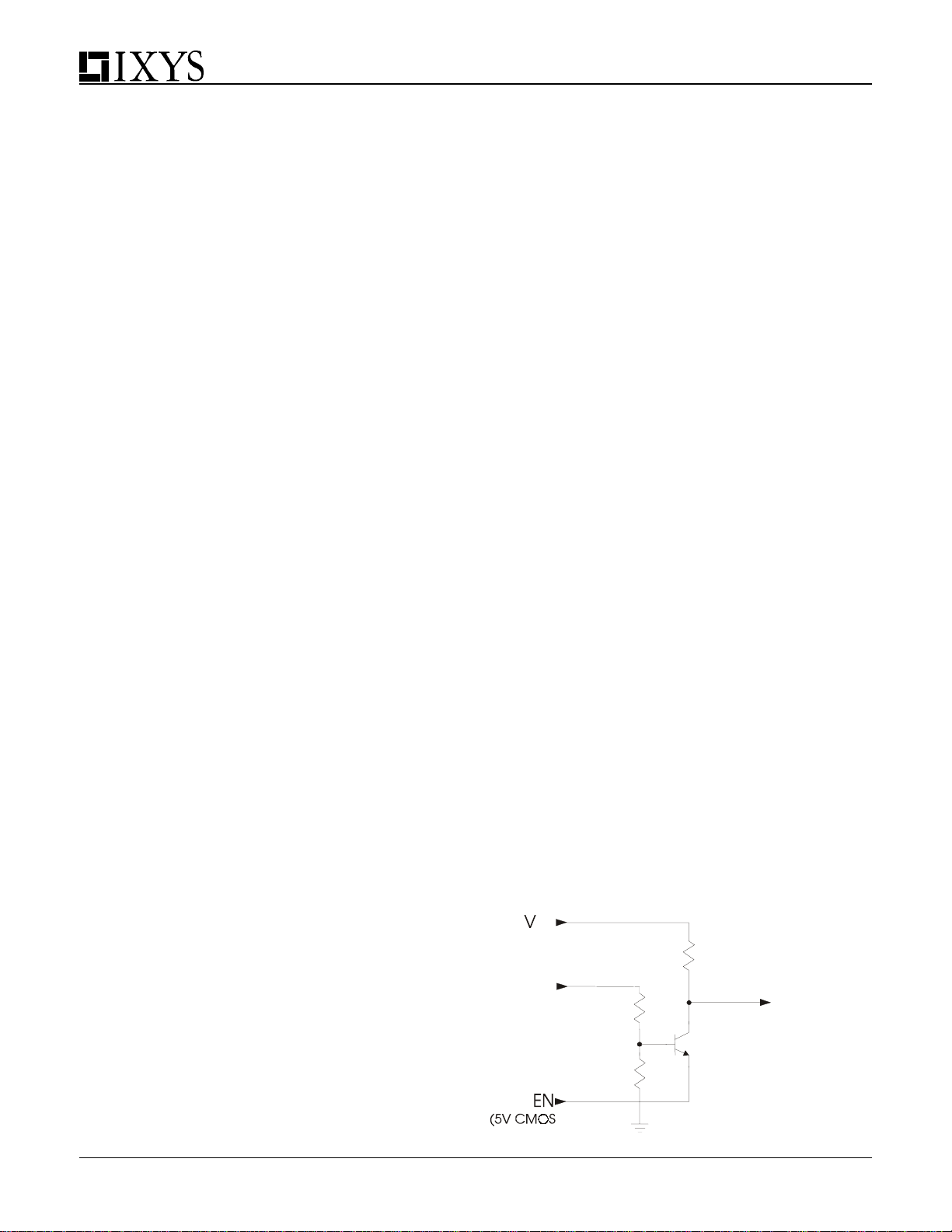
TTL to High Voltage CMOS Level Translation
When designing a circuit to drive a high speed MOSFET
utilizing the IXDD408, it is very important to keep certain design
criteria in mind, in order to optimize performance of the driver.
Particular attention needs to be paid to Supply Bypassing,
Grounding, and minimizing the Output Lead Inductance.
Say, for example, we are using the IXDD408 to charge a
5000pF capacitive load from 0 to 25 volts in 25ns…
Using the formula: I= ∆V C / ∆t, where ∆V=25V C=5000pF &
∆t=25ns we can determine that to charge 5000pF to 25 volts
in 25ns will take a constant current of 5A. (In reality, the charging
current won’t be constant, and will peak somewhere around
8A).
SUPPLY BYPASSING
In order for our design to turn the load on properly, the IXDD408
must be able to draw this 5A of current from the power supply
in the 25ns. This means that there must be very low impedance
between the driver and the power supply. The most common
method of achieving this low impedance is to bypass the
power supply at the driver with a capacitance value that is a
magnitude larger than the load capacitance. Usually, this
would be achieved by placing two different types of bypassing
capacitors, with complementary impedance curves, very close
to the driver itself. (These capacitors should be carefully
selected, low inductance, low resistance, high-pulse currentservice capacitors). Lead lengths may radiate at high frequency
due to inductance, so care should be taken to keep the lengths
of the leads between these bypass capacitors and the IXDD408
to an absolute minimum.
GROUNDING
In order for the design to turn the load off properly, the IXDD408
must be able to drain this 5A of current into an adequate
grounding system. There are three paths for returning current
that need to be considered: Path #1 is between the IXDD408
and it’s load. Path #2 is between the IXDD408 and it’s power
supply. Path #3 is between the IXDD408 and whatever logic
is driving it. All three of these paths should be as low in
resistance and inductance as possible, and thus as short as
practical. In addition, every effort should be made to keep these
three ground paths distinctly separate. Otherwise, (for
instance), the returning ground current from the load may
develop a voltage that would have a detrimental effect on the
logic line driving the IXDD408.
OUTPUT LEAD INDUCTANCE
Of equal importance to Supply Bypassing and Grounding are
issues related to the Output Lead Inductance. Every effort
should be made to keep the leads between the driver and it’s
load as short and wide as possible. If the driver must be placed
farther than 2” from the load, then the output leads should be
treated as transmission lines. In this case, a twisted-pair
should be considered, and the return line of each twisted pair
should be placed as close as possible to the ground pin of the
driver, and connect directly to the ground terminal of the load.
The enable (EN) input to the IXDD408 is a high voltage
CMOS logic level input where the EN input threshold is ½ V
and may not be compatible with 5V CMOS or TTL input levels.
,
CC
The IXDD408 EN input was intentionally designed for
enhanced noise immunity with the high voltage CMOS logic
levels. In a typical gate driver application, V
EN input threshold at 7.5V, a 5V CMOS logical high input
=15V and the
CC
applied to this typical IXDD408 application’s EN input will be
misinterpreted as a logical low, and may cause undesirable
or unexpected results. The note below is for optional
adaptation of TTL or 5V CMOS levels.
The circuit in Figure 28 alleviates this potential logic level
misinterpretation by translating a TTL or 5V CMOS logic input
to high voltage CMOS logic levels needed by the IXDD408 EN
input. From the figure, VCC is the gate driver power supply,
typically set between 8V to 20V, and VDD is the logic power
supply, typically between 3.3V to 5.5V. Resistors R1 and R2
form a voltage divider network so that the Q1 base is
positioned at the midpoint of the expected TTL logic transition
levels.
A TTL or 5V CMOS logic low, V
the Q1 emitter will drive it on. This causes the level translator
output, the Q1 collector output to settle to V
V
=<~2V, which is sufficiently low to be correctly
TTLLOW
interpreted as a high voltage CMOS logic low (<1/3VCC=5V for
=~<0.8V, input applied to
TTLLOW
CESATQ1
+
VCC =15V given in the IXDD408 data sheet.)
A TTL high, V
V
5VCMOSHIGH
Figure 28 will cause Q1 to be biased off. This results in Q1
=~>3.5V, applied to the EN input of the circuit in
=>~2.4V, or a 5V CMOS high,
TTLHIGH
collector being pulled up by R3 to VCC=15V, and provides a
high voltage CMOS logic high output. The high voltage CMOS
logical EN output applied to the IXDD408 EN input will enable
it, allowing the gate driver to fully function as an 8 Amp output
driver.
The total component cost of the circuit in Figure 28 is less
than $0.10 if purchased in quantities >1K pieces. It is
recommended that the physical placement of the level
translator circuit be placed close to the source of the TTL or
CMOS logic circuits to maximize noise rejection.
Figure 28 - TTL to High Voltage CMOS Level Translator
CC
(From Gate Driver
Power Supply)
V
DD
(From Logic
Power Supply)
3.3K
3.3K R2
R1
10K
R3
Q1
2N3904
High Voltage
CMOS
EN
Output
(To IXDD408
EN Input)
or
TTL
Input )
9
Page 10
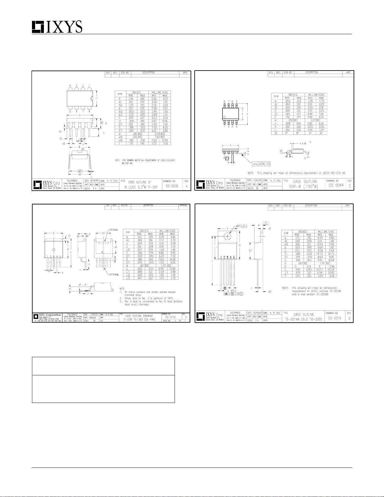
Package Information
IXDD408PI/408SI//408YI/408CI
NOTE: Mounting or solder tabs on all packages are connected to ground
Ordering Information
Part Numb er Package T ype T em p. Range
IXDD408PI 8-Pin PDIP
IXDD408SI 8-Pin SOIC
IXDD408YI 5-Pin TO-263
IXDD408CI 5-Pin TO-220
-40°C to +85°C
-40°C to +85°C
-40°C to +85°C
-40°C to +85°C
10
IXYS Corporation
3540 Bassett St; Santa Clara, CA 95054
Tel: 408-982-0700; Fax: 408-496-0670
e-mail: [email protected]
IXYS Semiconductor GmbH
Edisonstrasse15 ; D-68623; Lampertheim
Tel: +49-6206-503-0; Fax: +49-6206-503627
e-mail: [email protected]
Directed Energy, Inc.
An IXYS Company
2401 Research Blvd. Ste. 108
Ft. Collins, CO 80526
Tel: 970-493-1901; Fax: 970-493-1903
e-mail: [email protected]
Doc #9200-0227 R7
 Loading...