

Datasheet ILC5061M-46, ILC5061M-44, ILC5061M-31, ILC5061AM-26, ILC5061AM-46 Datasheet (Impala Linear Corporation)
...Page 1
ILC5061
SOT-23 Power Supply reset Monitor
Impala Linear Cor poration
Impala Linear Corporation
1
(408) 574-3939
www.impalalinear.com
June 1999
ILC5061 1.7
All-CMOS Monitor circuits in a 3-lead SOT-23 package offer the
best performance in power consumption and accuracy.
The ILC5061 comes in a series of ±1% accurate trip voltages to
fit most microprocessor applications. Even though its output
can sink 2mA, the device draws only 1µA in normal operation.
Additionally, a built-in hysteresis of 5% of detect voltage
simplifies system design.
• All-CMOS design in SOT-23 and SOT-89 package
• ±1% precision in Reset Detection
• Only 1µA of Iq
• 2mA of sink current capability
• Built-in hysteresis of 5% of detection voltage
• Voltage options of 2.6, 2.9, 3.1, 4.4, and 4.6V fit most
supervisory applications
• Microprocessor reset circuits
• Memory battery back-up circuitry
• Power-on reset circuits
• Portable and battery powered electronics
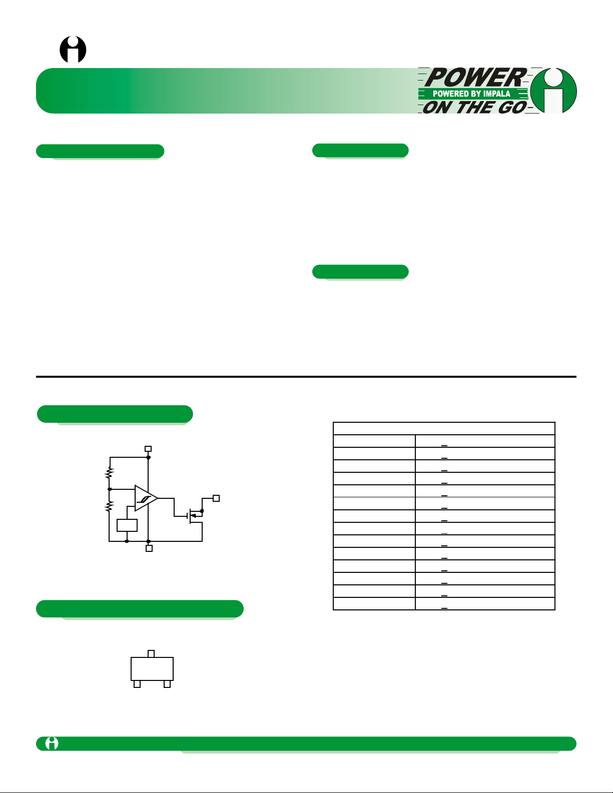
V
IN
V
SS
V
REF
V
OUT
Ordering Information*
ILC5061AM-26 2.6V+1% Monitor in SOT-23
ILC5061AM-27 2.7V+1% Monitor in SOT-23
ILC5061AM-28 2.8V+1% Monitor in SOT-23
ILC5061AM-29 2.9V+1% Monitor in SOT-23
ILC5061AM-31 3.1V+1% Monitor in SOT-23
ILC5061AM-44 4.4V+1% Monitor in SOT-23
ILC5061AM-46 4.6V+1% Monitor in SOT-23
ILC5061M-26 2.6V+2% Monitor in SOT-23
ILC5061M-27 2.7V+2% Monitor in SOT-23
ILC5061M-28 2.8V+2% Monitor in SOT-23
ILC5061M-29 2.9V+2% Monitor in SOT-23
ILC5061M-31 3.1V+2% Monitor in SOT-23
ILC5061M-44 4.4V+2% Monitor in SOT-23
ILC5061M-46 4.6V+2% Monitor in SOT-23
* Standard product offering comes in tape and reel,
quantity 3000 per reel orientation right
V
OUTVSS
V
IN
SOT -23
(TOP VI EW)
13
2
N-Channel Open Drain Output
General Description
Features
Applications
Block Diagram
Pin Package Configurations
Page 2
Impala Linear Corporation
2
(408) 574-3939
www.impalalinear.com
June 1999
ILC5061 1.7
Parameter
Symbol
Conditions
Min
Type
Max
Units
Detect Fail Voltage
VDF
A grade
VDF X 0.99
V
DF VDF
X 1.01
V
Detect Fail Voltage
VDF
Standard grade
VDF X 0.99
V
DF VDF
X 1.02
V
Hysteresis Range
V
HYS
VDF X 0.02
VDF X 0.05
VDF X 0.08
V
Supply Current
ISS
VIN = 1.5V
VIN = 2.0V
VIN = 3.0V
VIN = 4.0V
VIN = 5.0V
0.9
1.0
1.3
1.6
2.0
2.6
3.0
3.4
3.8
4.2
!
!
"A
Operating Voltage
VIN
VDF = 2.1~ 6.0V
1.5 10.0
V
Output Current
I
OUT
N-ch VDS = 0.5V
VIN = 1.0V
VIN = 2.0V
VIN = 3.0V
VIN = 4.0V
VIN = 5.0V
P-ch VDS = 2.1V
VIN = 8V
2.2
7.7
10.1
11.5
13.0
-10
mA
Temperature
Characteristics
#VDF/(#T
opr
!
VDF)
30oC <T
opr
<80oC
+100
Ppm/ oC
Delay Time Release
Voltage Output
Inversion)
T
DLY
(VDR V
OUT
inversion)
0.2
ms
Note:
1. An additional resistor between the VIN pin and supply voltage may cause deterioration of the characteristics due to increasing V
DR
.
Parameter
Symbol
Ratings
Units
Input Voltages
VIN
12
V
Output Current
I
OUT
50
mA
Output Voltages
V
OUT
VSS-0.3~+VIN+03
V
Continuous Total SOT-23
Power Dissipation
Pd
150
mW
Operation Ambient temperature
T
opr
-30~+80
o
C
Storage Temperature
T
stg
-40~+125
o
C
SOT-23 Power Supply reset Monitor
Absolute Maximum Ratings (TA=25οοC)
Electrical Characteristics (T
A
=25οοC)
Page 3

Impala Linear Corporation
3
(408) 574-3939
www.impalalinear.com
June 1999
ILC5061 1.7
The following designators 1~6 refer to the timing diagram below.
1. While the input voltage (V
IN
) is higher than the detect volt-
age (VDF), the V
OUT
output pin is at high impedance state.
2. When the input VIN voltage falls lower than VDF, V
OUT
drops near to ground voltage
3. If the input voltage further decreases below the minimum operating voltage (V
MIN
), the V
OUT
output becomes
unstable. In this condition, if the V
OUT
pin is pulled up,
V
OUT
indicates the VINvoltage.
4. During an increase of the input voltage from the V
SS
voltage, V
OUT
is not stable in the voltage below the V
MIN
.
Exceeding that level, the output stays at the ground level
(VSS) between the minimum operating voltage (V
MIN
) and
the detect release voltage (VDR).
5. If the input voltage increases more than VDR, then the
V
OUT
output pin is at high impedance state.
6. The difference between VDR and VDF is the hysteresis
in the system.
6
5
4
3
1
2
INPUT VOLTAGE (VIN)
DETECT RELEASE VOLTAGE (V
DR
)
DETECT FAIL VOLTAGE (V
DF
)
MINIMUM OPERATING VOLTAGE (V
MIN
)
GROUND VOLTAGE (V
SS
)
OUTPUT VOLTAGE (V
OUT
)
GROUND VOLTAGE (V
SS
)
SOT-23 Power Supply reset Monitor
Functional Description
Timing Diagram
Page 4

Impala Linear Corporation
4
(408) 574-3939
www.impalalinear.com
June 1999
ILC5061 1.7
OUTPUT VOLTAGE V
OUT
(V)
0
60
OUT P UT CUR RENT I
OUT
(mA)
1
80
10
0
2
VIN=4.0V
OUTPUT VOLTAGE vs OUTPUT CURRENT
ILC50 61
OUTPUT VOLT A GE V
OUT
(V)
0. 0
400
OUT P UT CUR RENT I
OUT
(µA)
800
1. 0
10 00
600
200
0.0
0.6
OUTPUT VOLTAGE vs OUTPUT CURRENT
ILC5061
3
4
3.5V
VIN=0.8 V
INP UT VO LTAG E VIN (V)
0
2. 0
I
DD
(µA)
4. 0
10
3. 0
1. 0
0
5
IDD vs INPUT VOLTAGE *
ILC5 06 1
T
opr
=8 0° C
25°C
20
30
40
50
70
3.0 V
2.5 V
2.0V
1.5V
0. 2 0. 4 0. 8
VIN=0.7 V
INP UT VO LTAG E VIN (V)
0
10
OUTP UT CURRENT I
OU T
(mA)
20
5
25
15
5
0
3
VDS=0. 5V
OUTPUT CURRENT vs INPUT VOLTAGE
ILC50 61
T
opr
=30°C
25 °C
12 34 6 7 8 9
-3 0°C
12 4
80 °C
* A sp ike of ½ to 1 µA may appear as Vi n crosses VDR or V DF
V
DS = 0.5V
SOT-23 Power Supply reset Monitor
Typical Performance Characteristics - general conditions for all curves
 Loading...