

Page 1
V
REF
V
OUT
V
SS
V
IN
查询ILC5061AIC23供应商
www.fairchildsemi.com
ILC5061
Power Supply reset Monitor with 1% Precision
Features
• All-CMOS design in SOT-23 or SC70 package
• ±1% precision in Reset Detection
• Only 1µA of Iq
• 2mA of sink current capability
• Built-in hysteresis of 5% of detection voltage
• Voltage options of 2.6, 2.9, 3.1, 4.4, and 4.6V fit most
supervisory applications
• Open-Drain Reset Output
Applications
• Microprocessor reset circuits
• Memory battery back-up circuitry
• Power-on reset circuits
• Portable and battery powered electronics
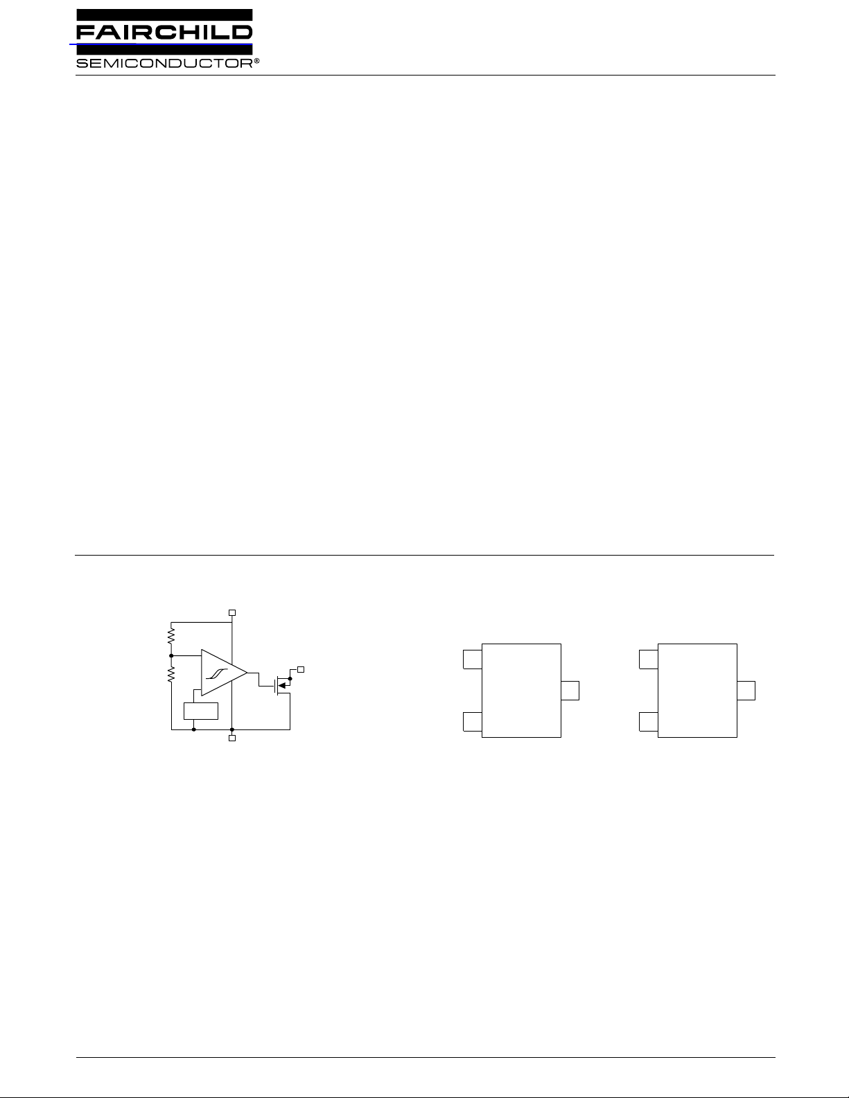
Block Diagram Pin Package Configurations
Description
All-CMOS Monitor circuits in either a 3-lead SOT-23 or
SC70 package offer the best performance in power consumption and accuracy.
The ILC5061 comes in a s eries o f ±1% accu rate trip voltages
to fit most microprocessor applications. Even thou gh its output can sink 2mA, the device draws only 1µA in normal
operation.
Additionally, a built-in hysteresis of 5% of detect voltage
simplifies system design.
Top View
1
V
OUT
3
V
SC-70
2
V
SS
IN
1
V
OUT
3
V
SOT-23
2
V
SS
IN
Rev. 2.5 1/2/03
Page 2
ILC5061 PRODUCT SPECIFICATION
ILC5061
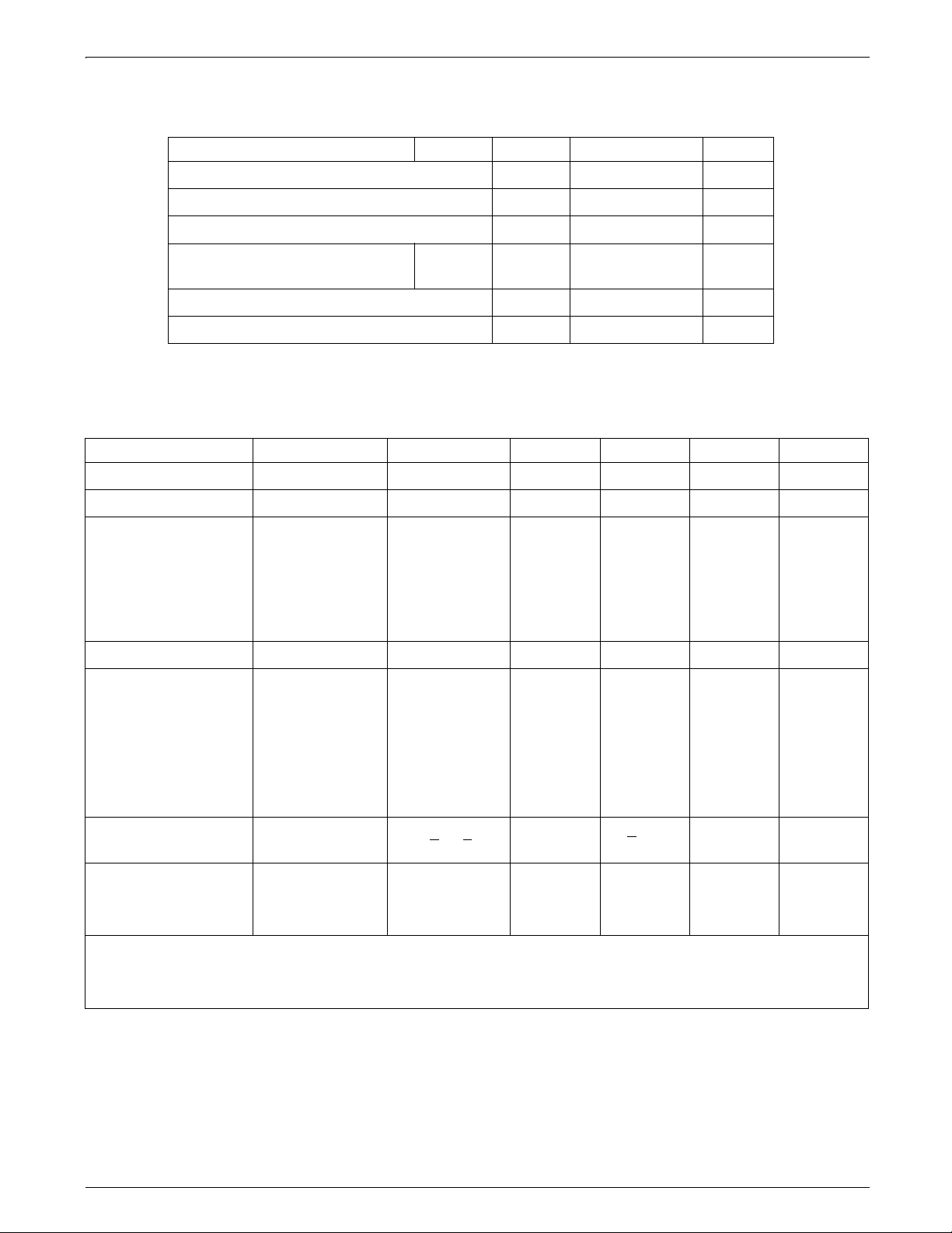
Absolute Maximum Ratings
Parameter Symbol Ratings Units
Input Voltages V
Output Current I
Output Voltages V
Continuous Total
SOT 23 P
Power Dissipation
Operation Ambient temperature T
Storage Temperature T
IN
OUT
OUT
opr
stg
VSS-0.3~+VIN+03 V
d
12 V
50 mA
150 mW
-30~+80
-40~+125
o
C
o
C
Electrical Characteristics T
Parameter Symbol Conditions Min Type Max Units
Detect Fail Voltage V
Hysteresis Range V
Supply Current I
Operating Voltage V
Output Current I
Temperature Charac-
DV
teristics
Delay Time Release
Voltage Output Inversion)
Note:
1. An additional resistor between the V
to increasing V
DR.
DF
HYS
SS
IN
OUT
/(DT
DF
opr
T
DLY
(VDR to V
inversion)
*
OUT
= 25°C
A
VDF X 0.99 V
DF
VDF X 1.01 V
VDF X 0.02 VDF X 0.05 VDF X 0.08 V
V
IN
V
IN
V
IN
V
IN
V
IN
= 1.5V
= 2.0V
= 3.0V
= 4.0V
= 5.0V
0.9
1.0
1.3
1.6
2.0
2.6
3.0
3.4
3.8
4.2
µA
VDF = 2.1~ 6.0V 1.5 10.0 V
N-ch VDS = 0.5V
V
= 1.0V
IN
V
= 2.0V
IN
V
= 3.0V
IN
V
= 4.0V
IN
V
= 5.0V
IN
VDF)
-30oC<T
opr
<80oC
-200 +100 +200
pin and supply voltage may cause deterioration of the characteristics due
IN
2.2
7.7
10.1
11.5
13.0
mA
Ppm/
0.1 ms
o
C
2 Rev. 2.5 1/2/03
Page 3
PRODUCT SPECIFICATION ILC5061
Functional Description
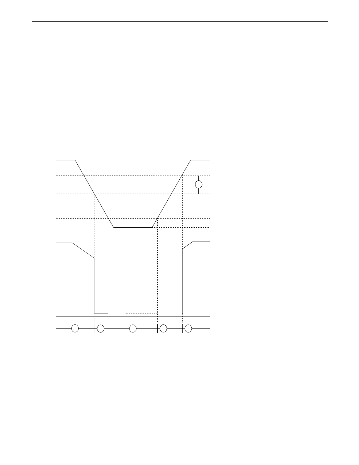
The following designators 1~6 refer to the timing diagram below.
1. While the input voltage ( V
state.
2. When the input V
voltage falls lower than VDF, V
IN
3. If the input voltage further decr eases below the minimu m operating voltage (V
unstable. In this condition, if the V
4. During an increase o f the i nput v oltage fr om the V
Exceeding that level , the outp ut s tay s a t the gr ound lev el ( V
and the detect release voltage (V
5. If the input voltage increases more than V
6. The difference between V
) is higher than the d etect voltag e (VDF), the V
IN
drops near to ground voltage
OUT
pin is pulled up, V
OUT
voltage, V
SS
).
DR
, then the V
DR
and VDF is the hysteresis in the system.
DR
indicates the VIN voltage.
OUT
is not stable i n the vo ltag e belo w the V
OUT
) between the minimum o per ati ng voltag e ( V
SS
output pin is at high impedance state.
OUT
output pin is at hig h impedance
OUT
MIN
), the V
output becomes
OUT
MIN
MIN
.
)
INPUT VOLTAGE (V
DETECT RELEASE VOLTAGE (V
6
DETECT FAIL VOLTAGE (V
MINIMUM OPERATING VOLTAGE (V
GROUND VOLTAGE (V
OUTPUT VOLTAGE (V
GROUND VOLTAGE (V
1
2
3
4
5
IN)
SS)
OUT)
SS)
DR)
DF)
MIN)
Rev. 2.5 1/2/03 3
Page 4
ILC5061 PRODUCT SPECIFICATION
µ
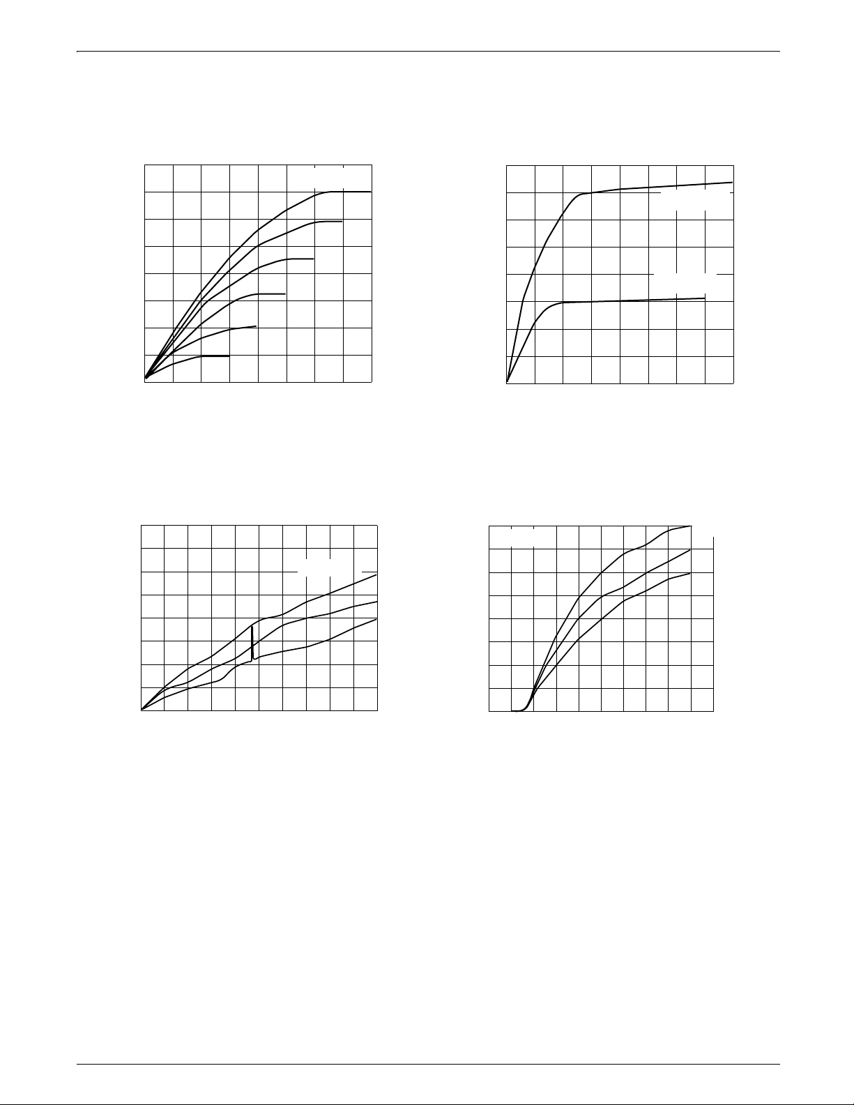
Typical Performance Characteristics
Output Voltage vs Output Current
ILC5061
80
70
60
50
40
30
20
OUTPUT CURRENT IOUT (mA)
10
2.0V
1.5V
0
0
12
OUTPUT VOLTAGE V
VIN = 4.0V
2.5V
OUT
3.0V
3
(V)
3.5V
4
Ordering Informatio n
ISS vs Input Voltage*
ILC5061
4.0
3.0
Topr = 80˚C
(General conditions for all curves)
Output Voltage vs Output Current
ILC5061
800
VIN = 0.8V
(µA)
600
OUT
400
200
OUTPUT CURRENT I
0
0
OUTPUT VOLTAGE VOUT (V)
Output Current vs Input Voltage
ILC5061
20
VDS = 0.5V
15
(mA)
OUT
0.2
0.4
VIN = 0.7V
0.6
T
25˚C
80˚C
opr
= -30˚C
0.8
(µA)
2.0
SS
I
1.0
0
0
* A spike of 1/2 to 1
25˚C
-30˚C
357
1
2
4
INPUT VOLTAGE VIN (V)
A may appear as VIN crosses VDR or V
6
9
8
10
DF
10
5
OUTPUT CURRENT I
0
0
1
2
INPUT VOLTAGE V
3
4
IN
(V)
5
4 Rev. 2.5 1/2/03
Page 5
PRODUCT SPECIFICATION ILC5061
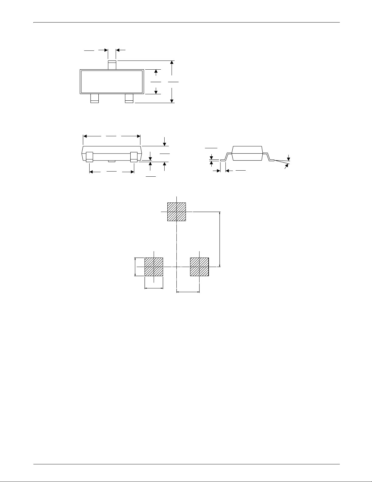
SOT-23 Package
0.021
0.015
0.098
0.055
0.083
0.047
0.120
0.105
0.0059
0.040
0.031
0.0035
0-8˚
0.079
0.071
0.004
0.001
PKG
C
L
0.76
0.76
LAND PATTERN RECOMMENDATION
0.95
0.010
0.005
2.29
Rev. 2.5 1/2/03 5
Page 6
ILC5061 PRODUCT SPECIFICATION
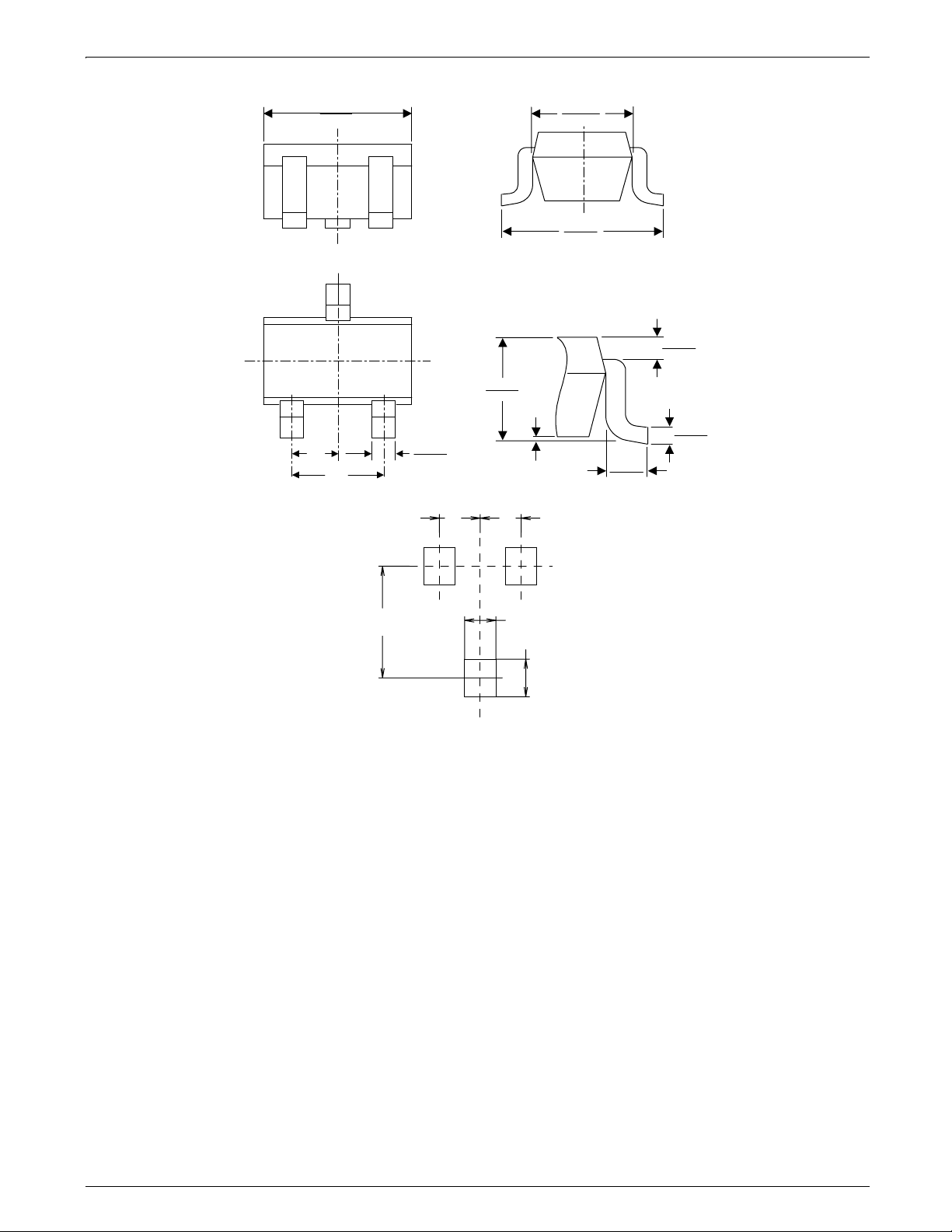
SC70 Package
.087 (2.2)
.071 (1.8)
.026
(.65)
.052
(1.3)
.016 (.40)
.012 (.30)
0.65
.043 (1.1)
.032 (.80)
0.65
.004 (.10)
.053 (1.35)
.045 (1.15)
.087 (2.2)
.079 (2.0)
.018 (.45)
.006 (.15)
.009 (.23)
.005 (.13)
.010 (.25)
.004 (.10)
1.80
0.5
0.6
Land Pattern Recommendation
6 Rev. 2.5 1/2/03
Page 7

PRODUCT SPECIFICATION ILC5061
Ordering Informatio n
PART
NUMBER
ILC5061AM23X M3AY 2.3 ± 1 % Open-Drain, active low 3-Pin, SOT23 3K units in T&R
ILC5061AM25X M5AY 2.5 ± 1 % Open-Drain, active low 3-Pin, SOT23 3K units in T&R
ILC5061AM26X M6AY 2.6 ± 1 % Open-Drain, active low 3-Pin, SOT23 3K units in T&R
ILC5061AM27X M7AY 2.7 ± 1 % Open-Drain, active low 3-Pin, SOT23 3K units in T&R
ILC5061AM28X M8AY 2.8 ± 1 % Open-Drain, active low 3-Pin, SOT23 3K units in T&R
ILC5061AM29X M9AY 2.9 ± 1 % Open-Drain, active low 3-Pin, SOT23 3K units in T&R
ILC5061AM31X N1AY 3.1 ± 1 % Open-Drain, active low 3-Pin, SOT23 3K units in T&R
ILC5061AM32X N2AY 3.2 ± 1 % Open-Drain, active low 3-Pin, SOT23 3K units in T&R
ILC5061AM34X N4AY 3.4 ± 1 % Open-Drain, active low 3-Pin, SOT23 3K units in T&R
ILC5061AM37X N7AY 3.7 ± 1 % Open-Drain, active low 3-Pin, SOT23 3K units in T&R
ILC5061AM44X P4AY 4.4 ± 1 % Open-Drain, active low 3-Pin, SOT23 3K units in T&R
ILC5061AM46X P6AY 4.6 ± 1 % Open-Drain, active low 3-Pin, SOT23 3K units in T&R
ILC5061M23X M3Y 2.3 ± 2 % Open-Drain, active low 3-Pin, SOT23 3K units in T&R
ILC5061M25X M5Y 2.5 ± 2 % Open-Drain, active low 3-Pin, SOT23 3K units in T&R
ILC5061M26X M6Y 2.6 ± 2 % Open-Drain, active low 3-Pin, SOT23 3K units in T&R
ILC5061M27X M7Y 2.7 ± 2 % Open-Drain, active low 3-Pin, SOT23 3K units in T&R
ILC5061M28X M8Y 2.8 ± 2 % Open-Drain, active low 3-Pin, SOT23 3K units in T&R
ILC5061M29X M9Y 2.9 ± 2 % Open-Drain, active low 3-Pin, SOT23 3K units in T&R
ILC5061M31X N1Y 3.1 ± 2 % Open-Drain, active low 3-Pin, SOT23 3K units in T&R
ILC5061M32X N2Y 3.2 ± 2 % Open-Drain, active low 3-Pin, SOT23 3K units in T&R
ILC5061M34X N4Y 3.4 ± 2 % Open-Drain, active low 3-Pin, SOT23 3K units in T&R
ILC5061M37X N7Y 3.7 ± 2 % Open-Drain, active low 3-Pin, SOT23 3K units in T&R
ILC5061M44X P4Y 4.4 ± 2 % Open-Drain, active low 3-Pin, SOT23 3K units in T&R
ILC5061M46X P6Y 4.6 ± 2 % Open-Drain, active low 3-Pin, SOT23 3K units in T&R
TOP
MARKING
RESET
THRESHOLD (V)
OUTPUT
TYPE
PACKAGE PACKING
METHOD
Note 1:Last digit in the "Top Marking" information (represented by "Y" in the above table) represents internal assembly lot
number
Note 2:Orientation of Tape & Reeled devices is Right.
Rev. 2.5 1/2/03 7
Page 8

ILC5061 PRODUCT SPECIFICATION
Ordering Informatio n
PART
NUMBER
TOP
MARKING
RESET
THRESHOLD (V)
OUTPUT
TYPE
PACKAGE PACKING
METHOD
ILC5061AIC23X M3AY 2.3 ± 1 % Open-Drain, active low 3-Pin, SC70 3K units in T&R
ILC5061AIC25X M5AY 2.5 ± 1 % Open-Drain, active low 3-Pin, SC70 3K units in T&R
ILC5061AIC26X M6AY 2.6 ± 1 % Open-Drain, active low 3-Pin, SC70 3K units in T&R
ILC5061AIC27X M7AY 2.7 ± 1 % Open-Drain, active low 3-Pin, SC70 3K units in T&R
ILC5061AIC28X M8AY 2.8 ± 1 % Open-Drain, active low 3-Pin, SC70 3K units in T&R
ILC5061AIC29X M9AY 2.9 ± 1 % Open-Drain, active low 3-Pin, SC70 3K units in T&R
ILC5061AIC31X N1AY 3.1 ± 1 % Open-Drain, active low 3-Pin, SC70 3K units in T&R
ILC5061AIC32X N2AY 3.2 ± 1 % Open-Drain, active low 3-Pin, SC70 3K units in T&R
ILC5061AIC34X N4AY 3.4 ± 1 % Open-Drain, active low 3-Pin, SC70 3K units in T&R
ILC5061AIC37X N7AY 3.7 ± 1 % Open-Drain, active low 3-Pin, SC70 3K units in T&R
ILC5061AIC44X P4AY 4.4 ± 1 % Open-Drain, active low 3-Pin, SC70 3K units in T&R
ILC5061AIC46X P6AY 4.6 ± 1 % Open-Drain, active low 3-Pin, SC70 3K units in T&R
ILC5061IC23X M3Y 2.3 ± 2 % Open-Drain, active low 3-Pin, SC70 3K units in T&R
ILC5061IC25X M5Y 2.5 ± 2 % Open-Drain, active low 3-Pin, SC70 3K units in T&R
ILC5061IC26X M6Y 2.6 ± 2 % Open-Drain, active low 3-Pin, SC70 3K units in T&R
ILC5061IC27X M7Y 2.7 ± 2 % Open-Drain, active low 3-Pin, SC70 3K units in T&R
ILC5061IC28X M8Y 2.8 ± 2 % Open-Drain, active low 3-Pin, SC70 3K units in T&R
ILC5061IC29X M9Y 2.9 ± 2 % Open-Drain, active low 3-Pin, SC70 3K units in T&R
ILC5061IC31X N1Y 3.1 ± 2 % Open-Drain, active low 3-Pin, SC70 3K units in T&R
ILC5061IC32X N2Y 3.2 ± 2 % Open-Drain, active low 3-Pin, SC70 3K units in T&R
ILC5061IC34X N4Y 3.4 ± 2 % Open-Drain, active low 3-Pin, SC70 3K units in T&R
ILC5061IC37X N7Y 3.7 ± 2 % Open-Drain, active low 3-Pin, SC70 3K units in T&R
ILC5061IC44X P4Y 4.4 ± 2 % Open-Drain, active low 3-Pin, SC70 3K units in T&R
ILC5061IC46X P6Y 4.6 ± 2 % Open-Drain, active low 3-Pin, SC70 3K units in T&R
Note 1: Last digit in the "Top Marking" information (represented by "Y" in the above table) represents internal assembly lot
Note 2: Orientation of Tape & Reeled devices is Right.
DISCLAIMER
FAIRCHILD SEMICONDUCTOR RESERVES THE RIGHT TO MAKE CHANGES WITHOUT FURTHER NOTICE TO
ANY PRODUCTS HEREIN TO IMPROVE RELIABILITY, FUNCTION OR DESIGN. FAIRCHILD DOES NOT ASSUME
ANY LIABILITY ARISING OUT OF THE APPLICATION OR USE OF ANY PRODUCT OR CIRCUIT DESCRIBED HEREIN;
NEITHER DOES IT CONVEY ANY LICENSE UNDER ITS PATENT RIGHTS, NOR THE RIGHTS OF OTHERS.
LIFE SUPPORT POLICY
FAIRCHILD’S PRODUCTS ARE NOT AUTHORIZED FOR USE AS CRITICAL COMPONENTS IN LIFE SUPPORT DEVICES
OR SYSTEMS WITHOUT THE EXPRESS WRITTEN APPROVAL OF THE PRESIDENT OF FAIRCHILD SEMICONDUCTOR
CORPORATION. As used herein:
1. Life support devices or systems are devices or systems
www.fairchildsemi.com
number
which, (a) are intended for surgical implant into the body,
or (b) support or sustain life, and (c) whose failure to
perform when properly used in accordance with
instructions for use provided in the labeling, can be
reasonably expected to result in a significant injury of the
user.
2. A critical component in any component of a life support
device or system whose failure to perform can be
reasonably expected to cause the failure of t he life support
device or system, or to affect its safety or effectiveness.
1/2/03 0.0m 001
 Loading...