

Page 1
查询ILC6363供应商
www.fairchildsemi.com
ILC6363
Step-Up DC-DC Converter for One-Cell Lithium-Ion
Batteries
Features
• ILC6363CIR-50: Fixed 5.0V output; custom voltages are
available upon request
• ILC6363CIR-ADJ: Adjustable output to 6V maximum
• Capable of 500mA output current
• Peak efficiency: > 90% at V
V
= 3.6V
IN
OUT
= 3.6V, I
= 300mA,
OUT
• No external diode is required (synchronous rectification)
• Battery input current of 300µA at no load
• True load disconnect from battery input in shutdown
(1µA)
• Oscillator frequency: 300kHz ±15%
• Low battery detector with 100ms transient rejection delay
• Power good output flag when V
is in regulation
OUT
• MSOP-8 package
Applications
• Cellular phones
• Palmtops, PDAs and portable electronics
• Equipment using single Lithium-Ion batteries
Description
The ILC6363 step-up/step-down DC-DC converter is a
switch mode converter, capable of supplying up to 500mA
output current, at a fixed or user selectable output voltage.
The range of input, and output voltage options makes the
ILC6363 ideal for Lithium-ion (Li-ion), or any other battery
application, where the input voltage range spans above and
below the regulated output voltage. When ILC6363’s input
voltage exceeds the output voltage by more than 800mV, the
output will begin to track the input linearly.
The ILC6363 is a direct replacement for ILC6360, in applications where SYNC pin is not used. The PFM or PWM
operating mode is user selectable through SEL pin connected
to ground or left open, respectively. The choice should be
dependent upon the current to be delivered to the load: PFM
is recommended for better efficiency at light load,while
PWM is recommended for more than 50mA load current.
In shutdown mode, the device allows true load disconnect
from battery input.
Configured as a 300kHz, fixed frequency PWM/PFM boost
converter , the ILC6363 can perform a limited b uck operation
in PFM mode, when the input voltage is up to 0.8V higher
than the output voltage.
The ILC6363 is unconditionally stable with no external
compensation; the sizes of the input and output capacitors
influence input and output ripple voltages, respectively.
Since the ILC6363 has an internal synchronous rectifier, the
standard fixed voltage version requires minimal external
components: an inductor, an input capacitor, and an output
capacitor. If a tantalum output capacitor is used, then an
additional 10µF ceramic output capacitor will help reduce
output ripple voltage.
Other features include a low battery input detector with a
built-in100ms transient rejection delay and a power good
indicator useful as a system power on reset.
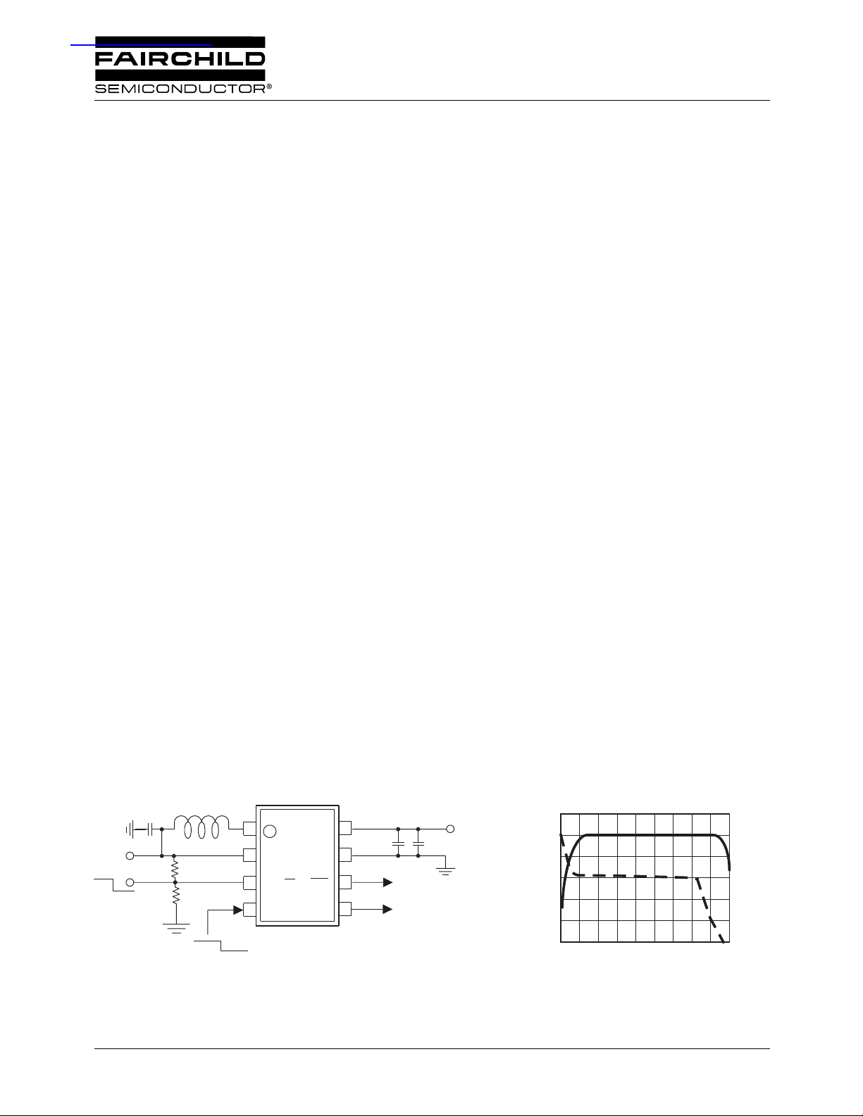
Typical Circuit
IN
V
IN
2.7V to 4.2V
ON
OFF
C
100µF
+
L
15µH
R5
R6
PWM
PFM
ILC6363CIR-XX
1
X
L
2
V
IN
3
LBI/SD
4
SEL
MSOP-8
Figure 1.
V
OUT
GND
LBO
POK
C
OUT
8
7
6
5
10µF 100µF
+
+
Low Battery
Detector Output
Power Good Output
(Fixed V
OUT
V
only)
OUT
Optimized to Maximize Battery Life
90
80
70
ILC6363 Efficiency (%)
Time
4.2
3.6
3.0
REV. 1.3.5 5/21/02
Battery Voltage (V)
Page 2
ILC6363 PRODUCT SPECIFICATION
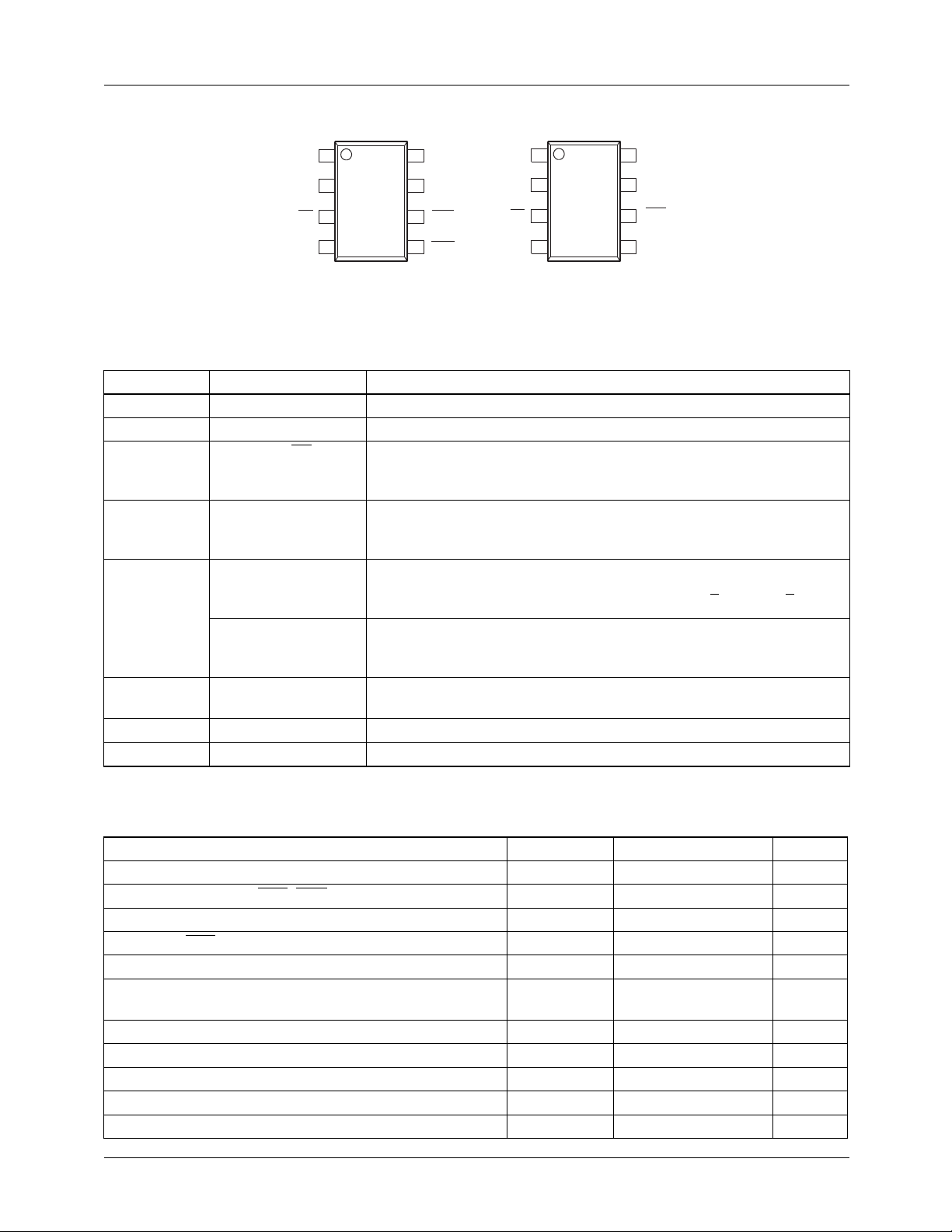
Pin Assignments
V
OUT
L
X
1
8
V
OUT
L
X
1
8
V
LB/SD
SEL
IN
2
3
4
(TOP VIEW)
ILC6363CIR-XX
MSOP
7
GND
LBO
6
5
POK
V
LB/SD
SEL
2
IN
3
4
MSOP
(TOP VIEW)
ILC6363CIR-ADJ
7
GND
LBO
6
5
V
FB
Pin Definitions
Pin Number Pin Name Pin Function Description
1L
2V
X
IN
3 LBI/SD
4 SEL
POK
(ILC6363CIR-XX
5
V
FB
(ILC6363CIR-ADJ)
6 LBO
7 GND
8V
OUT
Inductor input . Inductor L connected between this pin and the battery
Input Voltage . Connect directly to battery
Low battery detect input and shutdown . Low battery detect threshold
is set with this pin using a potential divider. If this pin is pulled to logic low
then the device will shutdown.
Select Input .
A low logic level signal applied to this pin selects PFM
operation mode. If the pin is left open or high logic level is applied, PWM
mode is selected.
Power Good Output . This open drain output pin will go high when
output voltage is within regulation, 0.92•V
0.98•V
OUT(NOM)
OUT(NOM)
Feedback Input . This pin sets the adjustable output voltage via an
external resistor divider network. The formula for choosing the resistors
is shown in the “Applications Information” section.
Low Battery Output . This open drain output will go low if the battery
voltage is below the low battery threshold set at pin 3.
Ground of the IC . Connect this pin to the battery and system ground
Regulated output voltage .
< V
threshold
<
Absolute Maximum Ratings
Parameter Symbol Ratings Units
Voltage on V
Voltage on LBI, Sync, LBO, POK, V
Peak switch current on L
Current on LBO pin I
Continuous total power dissipation at 85°C P
Short circuit current I
Operating ambient temperature T
Maximum junction temperature T
Storage temperature T
Lead temperature (soldering 10 sec.) 300 °C
Package thermal resistance
2
pin V
OUT
, L
and V
FB
X
pin IL
X
pins -0.3 to 7 V
IN
OUT
X
SINK(LBO)
D
SC
A
J(MAX)
stg
θ
JA
-0.3 to 7 V
1A
5mA
315 mW
Internally protected
(1 sec. duration)
-40 to 85 °C
150 °C
-40 to 125 °C
206 °C/W
REV. 1.3.5 5/21/02
A
Page 3
≥
η
≥
η
PRODUCT SPECIFICATION ILC6363
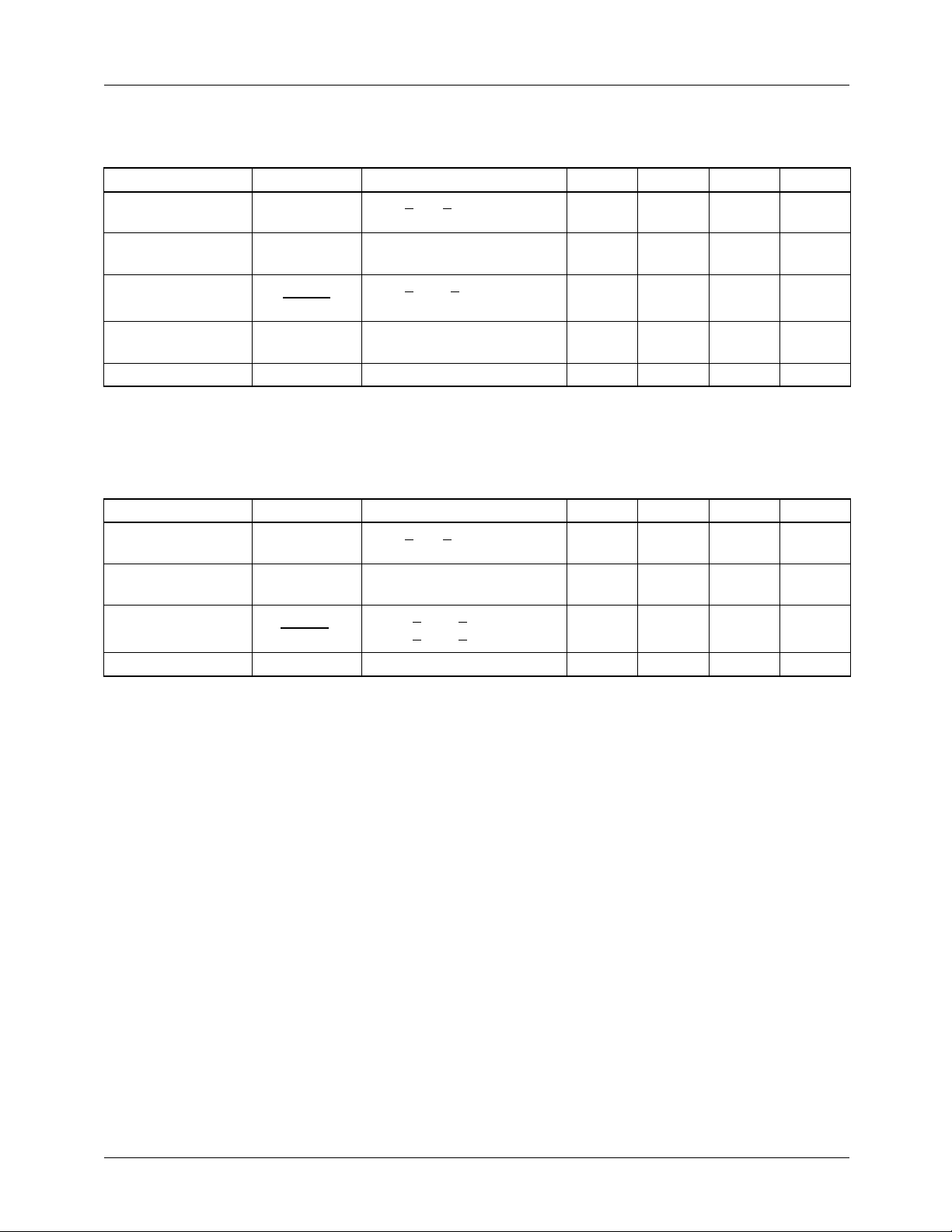
Electrical Characteristics ILC6363CIR-50 in PFM Mode
Unless otherwise specified, all limits are at V
IN
= V
= 3.6V, I
LBI
= 1mA and T
OUT
(SEL in LOW State)
= 25°C, test circuit Figure 1.
A
BOLDFACE type indicate limits over the specified operating temperature range. (Note 2)
Parameter Symbol Conditions Min. Typ. Max. Units
Output Voltage V
Maximum Output
Current
Load Regulation
No Load Battery
OUT(nom)
I
OUT
∆∆
∆∆
V
OUT
V
OUT
I
IN (no load)
2.7V <
V
OUT
V
= 2.7V
IN
1mA <
I
OUT
<
V
4.2V 4.875
IN
4.825
0.96V
OUT(nom)
I
50mA 1 %
<
OUT
,
5.0 5.125
5.175
250 mA
= 0mA 300 µA
Input Current
Efficiency
Electrical Characteristics ILC6363CIR-50 in PWM Mode
Unless otherwise specified, all limits are at V
I
= 20mA 85 %
OUT
(SEL Open)
= V
IN
= 3.6V, I
LBI
= 100mA and T
OUT
= 25°C, test circuit Figure 1.
A
BOLDFACE type indicate limits over the full operating temperature range. (Note 2)
Parameter Symbol Conditions Min. Typ. Max. Units
Output Voltage V
Maximum Output
OUT(nom)
I
OUT
2.7V < V
V
OUT
< 4.2V 4.850
IN
0.92V
OUT(nom)
4.800
5.0 5.150
5.200
500 mA
Current
Load Regulation
Efficiency
∆∆
∆∆
V
V
OUT
OUT
50mA < I
50mA < I
I
= 300mA 92 %
OUT
OUT
OUT
< 200mA
< 300mA
3
4
V
V
%
REV. 1.3.5 5/21/02
3
Page 4
ILC6363 PRODUCT SPECIFICATION
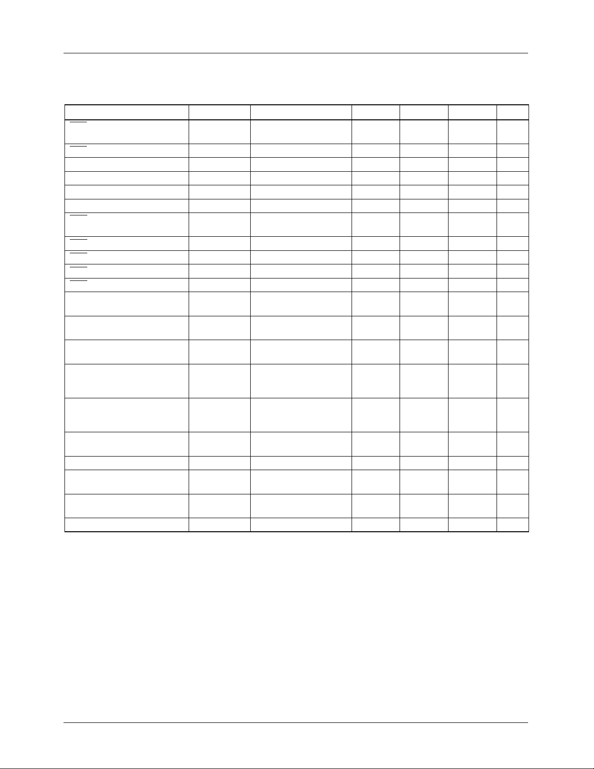
General Electrical Characteristics
T
= 25°C, V
A
BOLDFACE indicate limits over the specified operating temperature range. (Note 2).
output voltage low V
LBO
output leakage current I
LBO
Shutdown input voltage low V
Shutdown input voltage high V
SEL input voltage high V
SEL input voltage low V
output voltage low V
POK
output voltage high V
POK
output leakage Current I
POK
threshold V
POK
hysteresis V
POK
Feedback voltage
(ILC6363CIR-ADJ only)
Output voltage adjustment
range (ILC6363CIR-ADJ only)
Minimum startup voltage V
Input voltage range V
Battery input current in load
disconnect mode
Switch on resistance R
Oscillator frequency f
LBI input threshold V
Input leakage current I
LBI hold time t
Notes:
1. Absolute maximum ratings indicate limits which, when exceeded, may result in damage to the component. Electrical
specifications do not apply when operating the device outside its rated operating conditions.
2. Specified min/max limits are production tested or guaranteed through correlation based on statistical control methods.
Measurements are taken at constant junction temperature as close to ambient temperature as possible using low duty cycle
pulse testing.
3. Guaranteed by design
4. In order to get a valid low-battery-output (LBO) signal, the input voltage must be lower than the low-battery-input (LBI)
threshold for a duration greater than the low battery hold time (Hold(LBI)). This feature eliminates false triggering due to
voltage transients at the battery terminal.
= V
IN
= 3.6V, I
LBI
= 50mA, unless otherwise specified.
OUT
Parameter Symbol Conditions Min. Typ. Max. Units
I
LBO(low)
LBO(hi)
SD(low)
SD(hi)
SEL(hi)
SEL(low)
POK(low)
POK(hi)
L(POK)
TH(POK
HYST
V
FB
V
OUT(ADJ) min
V
OUT(ADJ) max
I
IN(start)
IN
I
IN(SD)
ds(on)
osc
REF
LEAK
HOLD(LBI)
= 2mA, open drain
SINK
output, V
V
LBO
= 1V
LBI
= 5V 1
16
1.5 V
I
= 2mA, open drain
SINK
output
6V at pin 5 2 µA
0.92xV
OUT
0.95xV
OUT
50 mV
1.225
1.250 1.275
1.212
VIN = 0.9V, I
V
= 3V, I
IN
= 10mA, PWM
OUT
OUT
OUT
= 50mA
= 50mA
2.5
6
0.9 1 V
mode
V
OUT
± 4%
I
OUT
V
LBI/SD
V
OUT
= V
OUT(nominal)
= 10mA
< 0.4V,
= 0V
0.9
1
1 10 µA
(short circuit)
N-Channel MOSFET
P-Channel MOSFET
400
750
255 300 345 kHz
1.175
1.250 1.325
1.150
Pins LB/SD,SEL and
VFB, (Note 3)
(Note 4) 100 120 mS
0.4
0.4
0.4 V
0.4 V
6 V
0.98xV
OUT
1.288
V
OUT(nomi-
+ 0.8V
nal)
1.350
200 nA
V
µA
V
V
V
V
V
V
mΩ
V
2
4
REV. 1.3.5 5/21/02
Page 5
PRODUCT SPECIFICATION ILC6363
Application Information
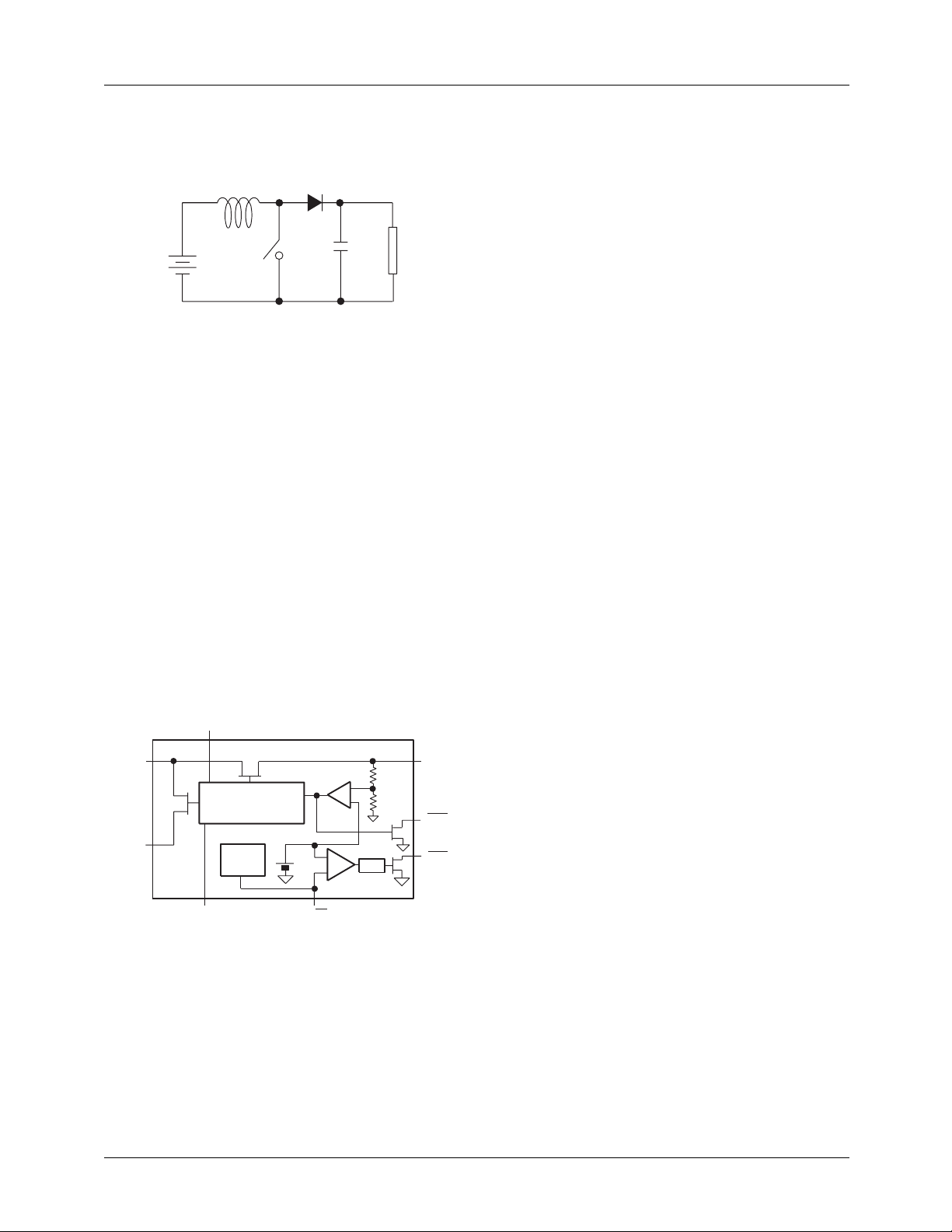
The ILC6363 performs boost DC-DC conversion by controlling the switch element as shown in the simplified circuit in
Figure 3 below.
Figure 3. Basic Boost Circuit
When the switch is closed, current is built up through the
inductor. When the switch opens, this current is forced
through the diode to the output. As this on and off switching
continues, the output capacitor voltage builds up due to the
charge it is storing from the inductor current. In this way, the
output voltage is boosted relative to the input.
In general, the switching characteristic is determined by the
output voltage desired and the current required by the load.
The energy transfer is determined by the power stored in the
coil during each switching cycle.
PL = ƒ(tON, VIN)
Synchronous Rectification
The ILC6363 also uses a technique called “synchronous
rectification” which removes the need for the external diode
used in other circuits. The diode is replaced with a second
switch or in the case of the ILC6363, an FET as shown in
Figure 4 below.
V
IN
ILC6363
-
+
+
DELAY
-
V
OUT
POK
LBO
PWM/PFM
CONTROLLER
SHUTDOWN
CONTROL
SEL
SW2
V
REF
LB/SD
L
X
SW1
GND
Figure 4. Simplified ILC6383 block diagram
The two switches now open and close in opposition to each
other, directing the flow of current to either char ge the inductor or to feed the load. The ILC6363 monitors the voltage on
the output capacitor to determine how much and how often
to drive the switches.
PWM Mode Operation
The ILC6363 uses a PWM or Pulse Width Modulation
technique. The switches are constantly driven at typically
300kHz. The control circuitry varies the power being
delivered to the load by varying the on-time, or duty cycle,
of the switch SW1 (see Figure 5). Since more on-time
translates to higher current build-up in the inductor, the
maximum duty cycle of the switch determines the maximum
load current that the device can support. The minimum value
of the duty cycle determines the minimum load current that
can maintain the output voltage within specified values.
There are two key advantages of the PWM type controllers.
First, because the controller automatically varies the duty
cycle of the switch's on-time in response to changing load
conditions, the PWM controller will always have an optimized waveform for a steady-state load. This translates to
very good efficiency at high currents and minimal ripple on
the output. Ripple is due to the output cap constantly accepting and storing the charge received from the inductor, and
delivering charge as required by the load. The “pumping”
action of the switch produces a sawtooth-shaped voltage as
seen by the output.
The other key advantage of the PWM type controllers over
pulse frequency modulated (PFM) types is that the radiated
noise due to the switching transients will always occur at
(fixed) switching frequency. Many applications do not care
much about switching noise, but certain types of applications, especially communication equipment, need to minimize the high frequency interference within their system as
much as possible. Use of the PWM converter in those cases
is desirable.
PFM Mode Operation
For light loads the ILC6363 can be switched to PFM. This
technique conserves power by only switching the output if
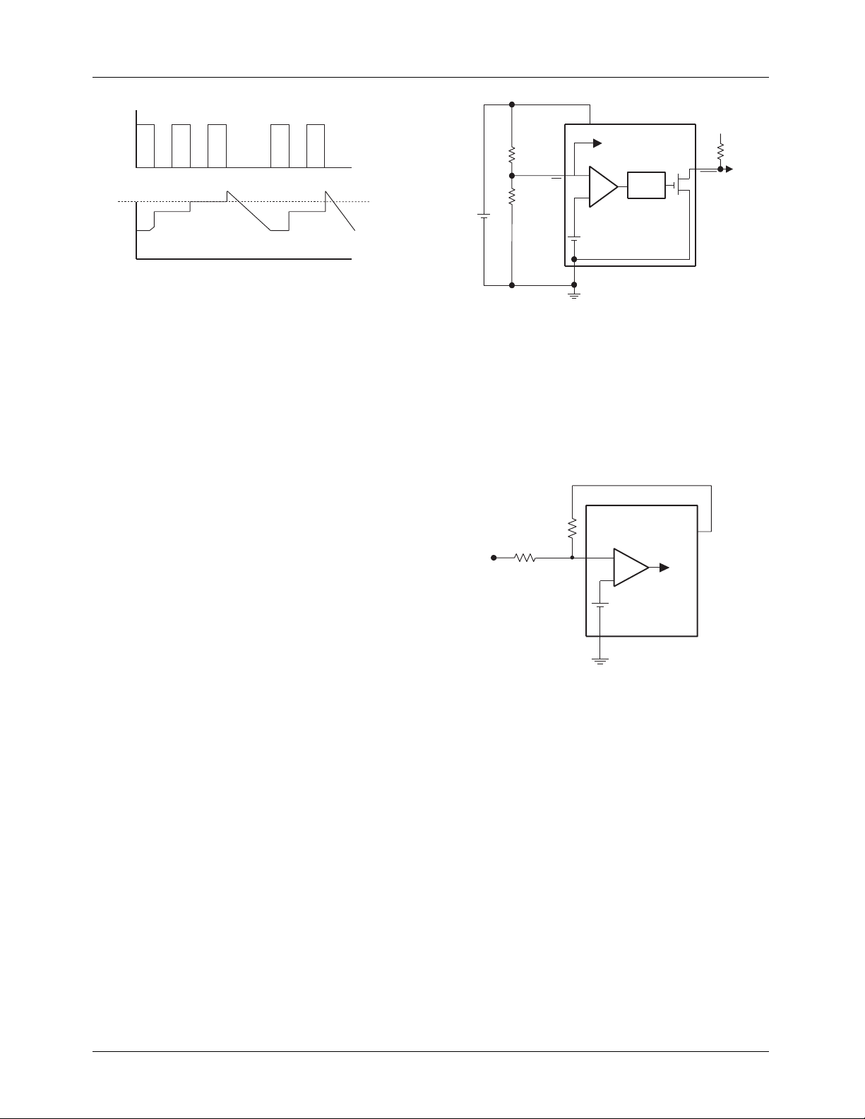
the current drain requires it. As shown in the Figure 5, the
waveform actually skips pulses depending on the power
needed by the output. This technique is also called “pulse
skipping” because of this characteristic.
In the ILC6363, the switchover from PWM to PFM mode is
determined by the user to improve efficiency and conserve
power.
The Dual PWM/PFM mode architecture was designed specifically for applications such as wireless communications,
which need the spectral predictability of a PWM-type
DC-DC converter, yet also need the highest efficiencies
possible, especially in Standby mode.
REV. 1.3.5 5/21/02 5
Page 6
ILC6363 PRODUCT SPECIFICATION
Switch Waveform
V
SET
V
OUT
Figure 5. PFM Waveform
Other Considerations
The other limitation of PWM techniques is that, while the
fundamental switching frequency is easier to filter out since
it's constant, the higher order harmonics of PWM will be
present and may have to be filtered out, as well. An y filtering
requirements, though, will vary by application and by actual
system design and layout, so generalizations in this area are
difficult, at best.
However, PWM control for boost DC-DC conversion is
widely used, especially in audio-noise sensitive applications
or applications requiring strict filtering of the high frequency
components.
Low Battery Detector
The ILC6363's low battery detector is a based on a CMOS
comparator. The negative input of the comparator is tied to
an internal 1.25V (nominal) reference, V
input is the LBI/SD pin. It uses a simple potential divider
arrangement with two resistors to set the LBI threshold as
shown in Figure 6. The input bias current of the LBI pin is
only 200nA. This means that the resistor values R1 and R2
can be set quite high. The formula for setting the LBI
threshold is:
. The positive
REF
V
IN
R5
R6
LBI/SD
3
2
+
-
1.25V
Internal
Reference
GND7
Shutdown
DELAY
100ms
ILC6363
R
6
LBO
3.3V
PU
Figure 6. Low Battery Detector
The output of the low battery detector is an open drain
capable of sinking 2mA. A 10kΩ pull-up resistor is
recommended on this output.
For V
< 1.25V
LBI
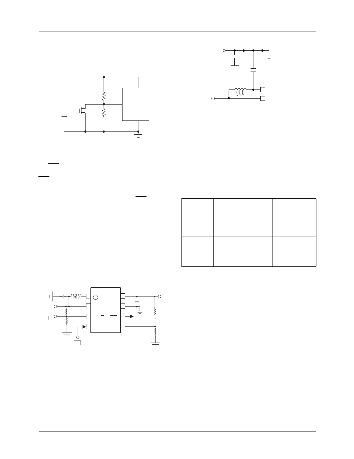
The low battery detector can also be configured for voltages
<1.25V by bootstrapping the LBI input from V
OUT
. The
circuitry for this is shown in Figure 7.
ILC6363
R2
V
IN
R1
3
LBI/SD
Figure 7. V
+
-
1.25V
Internal
Reference
GND7
< 1.25V
LBI
8
V
OUT
VLBI = VREF x (1+R5/R6)
Since the LBI input current is negligible (<200nA), this
equation is derived by applying voltage divider formula
across R6. A typical value for R6 is 100kΩ.
R5 = 100kΩ x [(VLBI/VREF) -1],
where VREF=1.25V (nom.)
The LBI detector has a built in delay of 120ms. In order to
get a valid low-battery-output (LBO) signal, the input voltage must be lower than the low-battery-input (LBI) threshold
for a duration greater than the low battery hold time
(t
hold(LBI)
) of 120msec. This feature eliminates false triggering due to voltage transients at the battery terminal caused by
high frequency switching currents.
The following equation is used when VIN is lower than
1.25V:
R1 = R2 x [(V
where V
= 1.25V (nom.)
REF
– VIN) / (V
REF
OUT
– V
REF
)],
This equation can also be derived using voltage divider
formula across R2. A typical value for R2 is 100kΩ.
Shut Down
The LBI pin is shared with the shutdown pin. A low voltage
(<0.4V) will put the ILC6363 into a power down state. The
simplest way to implement this is with an FET across R6 as
shown in Figure 8. Note that when the device is not in PWM
mode or is in shutdown the low battery detector does not
operate.
6 REV. 1.3.5 5/21/02
Page 7
PRODUCT SPECIFICATION ILC6363
When the ILC6363 is shut down, the synchronous rectifier
disconnects the output from the input. This ensures that there
is only leakage (IIN < 1µA typical) from the input to the output so that the battery is not drained when the ILC6363 is
shut down.
V
IN
2
ILC6363
3
LBI/SD
7 GND
ON/OFF
R5
R6
Figure 8. Shut Down Control
Power Good Output (POK)
The POK output of the ILC6363 indicates when V
within the regulation tolerance of the set output voltage.
POK output is an open drain device output capable of sinking 2mA. It will remain pulled low until the output voltage
has risen to typically 95% of the specified V
OUT
pull-up resistor must be connected from the POK output
(pin 5 of ILC6363CIR-XX) to either ILC6363’s output or to
some other system voltage source.
is
OUT
. Note that a
Adjustable Output Voltage Selection
The ILC6363-ADJ allows the output voltage to be set using
a potential divider. The formula for setting the adjustable
output voltage is;
V
= VFB x (1+R1/R2), R1+R2 ≤ 100kΩ
OUT
1A Schottky Diodes
-V
0.01µF
0.01µF
L
V
IN
1
2
ILC6363
X
L
IN
V
Figure 10. Negative Output Voltage
External Component Selection
Inductors
The ILC6363 is designed to work with a 15µH inductor in
most applications. There are several vendors who supply
standard surface mount inductors to this value. Suggested
suppliers are shown in table 1. Higher values of inductance
will improve efficienc y , but will reduce peak inductor current
and consequently ripple and noise, but will also limit output
current.
Vendor Part Number Contact
Coilcraft D03316P-153
D01608C-153
muRata LQH4N150K
LQH3C150K
Sumida CDR74B-150MC
CD43-150
CD54-150
TDK NLC453232T-150K (847) 390-4373
(847) 639-6400
(814) 237-1431
(847) 956-0666
Where VFB is the threshold set which is 1.25V nominal.
PFM
ILC6363-ADJ
1
2
V
IN
3
LBI/SD
4
SEL
L
X
MSOP-8
V
OUT
GND
LBO
V
V
8
+
7
6
5
FB
V
OUT
OUT
100µF
C
OUT
R1
R2
= 1.25 (1+R1/R2)
C
IN
100µF
IN
V
1 to 3-cell R5
ON
OFF
L
15mH
R6
PWM
Figure 9. Adjustable Voltage Configuration
Negative V oltage Output
It is possible to generate a negative output voltage as a
secondary supply using the ILC6363. This negative voltage
may be useful in some applications where a negative bias
voltage at low current is required.
Capacitors
Input Capacitor
The input capacitor is necessary to minimize the peak
current drawn from the battery. Typically a 100µF tantalum
capacitor is recommended. Low equivalent series resistance
(ESR) capacitors will help to minimize battery voltage
ripple.
Output Capacitor
Low ESR capacitors should be used at the output of the
ILC6363 to minimize output ripple. The high switching
speeds and fast changes in the output capacitor current, mean
that the equivalent series impedance of the capacitor can
contribute greatly to the output ripple. In order to minimize
these effects choose an output capacitor with less than 10nH
of equivalent series inductance (ESL) and less than 100mΩ
of equivalent series resistance (ESR). Typically these
characteristics are met with ceramic capacitors, but may also
be met with certain types of tantalum capacitors. Suitable
vendors are shown in the following table.
REV. 1.3.5 5/21/02 7
Page 8
PRODUCT SPECIFICATION ILC6363
Description Vendor Contact
T495 series tantalum Kemet (864) 963-6300
595D series tantalum Sprague (603) 224-1961
TAJ, TPS series
AVX (803) 946-0690
tantalum
X5R Ceramic
X7R Ceramic
TDK (847) 390-4373
AVX (803) 946-0690
muRata www.murata.com
Layout and Grounding
Considerations
High frequency switching and large peak currents means
PCB design for DC-DC converters requires careful
consideration. As a general rule place the DC-DC converter
circuitry well away from any sensitive RF or analog components. The layout of the DC-DC converters and its external
components are also based on some simple rules to minimize
EMI and output voltage ripple.
Layout
1. Place all power components, ILC6363, inductor, input
capacitor and output capacitor as close together as
possible.
2. Keep the output capacitor as close to the ILC6363 as
possible with very short traces to the V
pins. Typically it should be within 0.25 inches or 6mm.
and GND
OUT
3. Keep the traces for the power components wide,
typically >50mil or 1.25mm.
4. Place the external networks for LBI and VFB close to
the ILC6363, but away from the power components as
far as possible.
Grounding
1. Use a star grounding system with separate traces for
the power ground and the low power signals such as
LBI/SD
the power supply enters the PCB.
2. On multilayer boards use component side copper for
grounding around the ILC6363 and connect back to a
quiet ground plane using vias.
and VFB. The star should radiate from where
C
IN
100µF
15L1µH
V
IN
ON/OFF
PWM
PFM
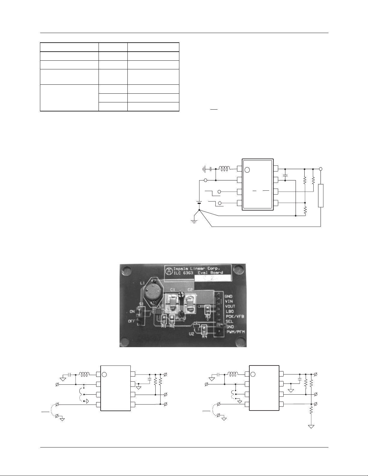
Figure 11. Recommended Application Circuit
Schematic for ILC6363CIR-ADJ
ILC6363
1
L
X
V
OUT
2
V
IN
GND
3
LBI/SD
LBO
4
SEL
V
FB
Local "Quiet" Ground
Power Ground
8
OUT
C
+
100µF
7
6
5
R1
R2
V
R3
OUT
Load
1
2
V
IN
3
LBI
4
SEL
U1
ILC6363ADJ
X
L
GND
POK/VFB
V
LBO
OUT
8
C1
100µF
7
6
5
R3
10K
V
OUT
R1
LBO
VFB
R2
PWM
PFM
SEL
GND
U1
ILC6363XX
L1
100µF
C2
IN
V
15µH
ON
OFF
1
2
VIN
3
LBI
4
SEL
L
X
OUT
V
GND
LBO
POK/VFB
8
C1
100µF
7
6
5
R3
10K
R1
10K
VOUT
LBO
POK
V
IN
PWM
PFM
C2
SEL
GND
L1
100µF
15µH
ON
OFF
NOTE: R1 and R2 are user determined values to set
V
OUT
= VFB(1+R1/R2)
R1+R2 ≤ 100kΩ
REV. 1.3.5 5/21/02 8
Page 9

ILC6363 PRODUCT SPECIFICATION
Evaluation Board Parts List for Printed Circuit Board Shown on the Previous Page
Label Part Number Manufacturer Description
U1 ILC6363CIR-ADJ Fairchild Semiconductor DC-DC converter
C GRM44-1 X5R 107K 6.3 muRata 100µF, ceramic capacitor
L1 LQS66C150M04 muRata 15µH, 1.3A
R1 and R2 — Dale, Panasonic User determined values
R3 — Dale, Panasonic 10kΩ, 1/10W, SMT
Label Part Number Manufacturer Description
U1 ILC6363CIR-XX Fairchild Semiconductor DC-DC converter
C GRM44-1 X5R 107K 6.3 muRata 100µF, ceramic capacitor
L1 LQS66CA150M04 muRata 15µH, 1.3A
R1 and R3 - Dale, Panasonic 10kΩ, 1/10W, SMT
9 REV. 1.3.5 5/21/02
Page 10
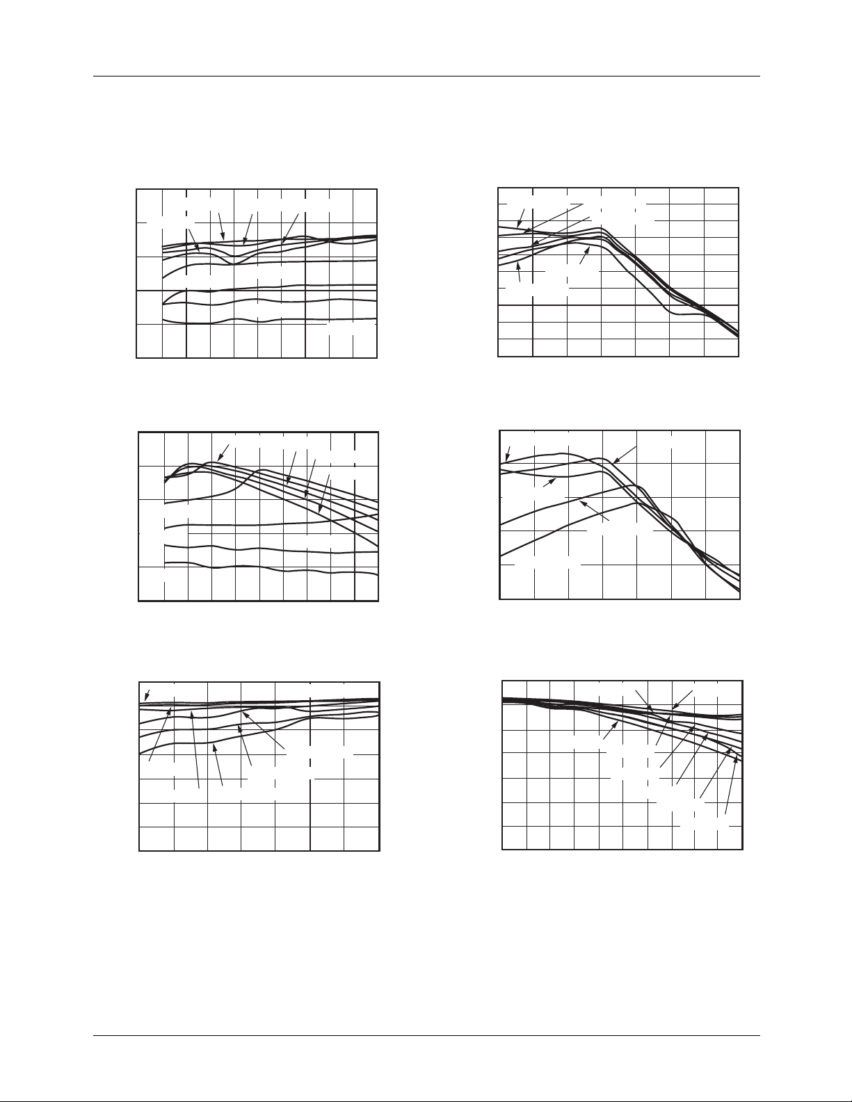
ILC6363 PRODUCT SPECIFICATION
Typical Performance Characteristics ILC6363CIR-ADJ
Unless otherwise specified: TA = 25°C, CIN = 100µF, C
= 100µF, L = 15µH, V
OUT
OUT
= 3.6V
Efficiency vs Output Current (PFM Mode)
100
95
VIN=3.4V
VIN=2.8V
VIN=3.2V
VIN=3V
90
I
OUT
VIN=3.6V
VIN=4V
VIN=4.2V
30 40 50
(mA)
85
VIN=3.8V
Efficiency (%)
80
75
01020
Efficiency vs Output Current (PWM Mode)
100
95
90
VIN=3.6V
85
VIN=3.8V
Efficiency (%)
80
VIN=4.2V
75
0 100 200
VIN=3.4V
(mA)
I
OUT
VIN=3.2V
VIN=3.0V
VIN=2.8V
VIN=4.0V
300 400 500
Efficiency vs Input Voltage (PFM Mode)
98
I
96
94
OUT
=50mA
I
OUT
I
OUT
=40mA
=10mA
92
90
I
88
86
I
OUT
84
Efficiency (%)
OUT
=20mA
=5mA
82
80
78
2.8 3.0 3.2
3.4 3.6 3.8 4.0 4.2
V
(V)
IN
Efficiency vs Input Voltage (PWM Mode)
98
I
=100mA
OUT
94
I
=50mA
OUT
90
86
Efficiency (%)
I
OUT
82
78
2.8 3.0 3.2
=500mA
I
OUT
3.4 3.6 3.8 4.0 4.2
=400mA
(V)
V
IN
I
OUT
=200mA
Line Regulation Load Regulation
3.7
I
OUT
3.6
3.5
3.4
(V)
I
=50mA
OUT
3.3
OUT
V
I
=200mA
OUT
3.2
3.1
3.0
2.8 3.0 3.2
=3mA
V
=(nom)=3.6V
OUT
I
=300mA
OUT
I
=400mA
OUT
I
=500mA
OUT
3.4 3.6 3.8 4.0 4.2
(V)
V
IN
3.7
VIN=4.0V
VIN=4.2V
3.6
3.5
3.4
(V)
3.3
OUT
V
VIN=2.8V
3.2
3.1
3.0
0 50 100 150 200 250 300 350400 450 500
VIN=3.8V
VIN=3.6V
I
OUT
VIN=3.4V
VIN=3.2V
VIN=3.0V
(mA)
10 REV. 1.3.5 5/21/02
Page 11
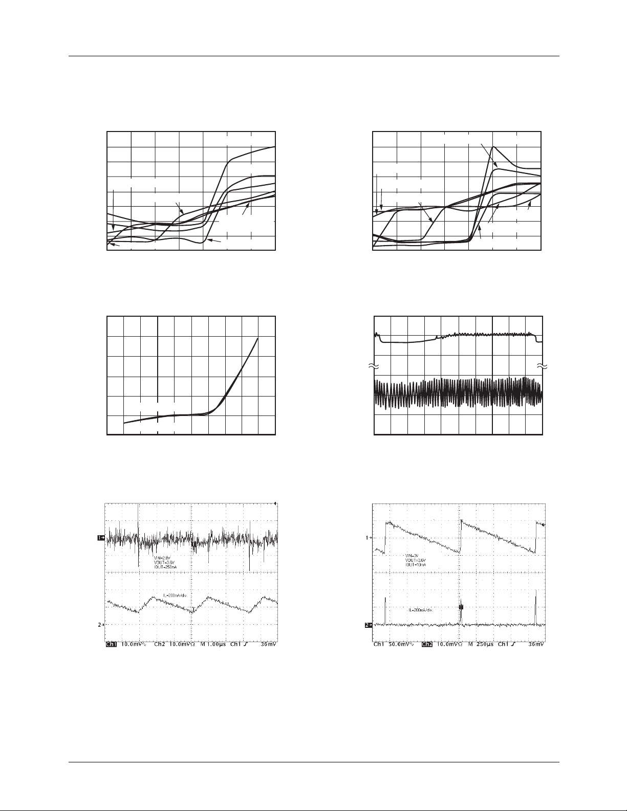
PRODUCT SPECIFICATION ILC6363
Typical Performance Characteristics ILC6363CIR-ADJ
Unless otherwise specified: TA = 25°C, CIN = 100µF, C
= 100µF, L = 15µH, V
OUT
OUT
= 3.6V
Output Ripple Voltage vs Input Voltage
160
140
120
100
I
=0mA, 10mA
OUT
80
60
I
=100mA I
OUT
40
Output Ripple (mVpp)
20
I
=50mA
OUT
0
2.8 3.0 3.2
4.6
4.2
(V)
OUT
V
3.8
I
=250mA
2.8
OUT
I
=500mA
OUT
3.4 4.0 4.6 5.2
3.6
3.4
3.4 3.6 3.8 4.0 4.2
V
IN
VIN vs V
V
IN
(V)
(V)
OUT
I
=500mA
OUT
I
OUT
I
=0mA, 10mA
OUT
I
OUT
50mA
=200mA
=400mA
Ripple Current vs Input Voltage
160
140
120
I
=0mA
OUT
100
I
=10mA
OUT
80
60
OUT
=100mA
40
Ripple Current (mApp)
20
0
2.8 3.0 3.2
Line Transient Response
3.8
(mV)
IN
2.8
+50
(mV) V
0
OUT
-50
V
I
OUT
=400mA
I
OUT
I
OUT
I
OUT
I
OUT
=200mA
=500mA
=100mA
=50mA
3.4 3.6 3.8 4.0 4.2
(V)
V
IN
500µs/div
PWM Mode Load Switching Waveform
OUT
V
AC Coupled
Current
Inductor
PFM Mode Load Switching Waveform
OUT
V
AC Coupled
Current
Inductor
250µs/div1µs/div
REV. 1.3.5 5/21/02 11
Page 12
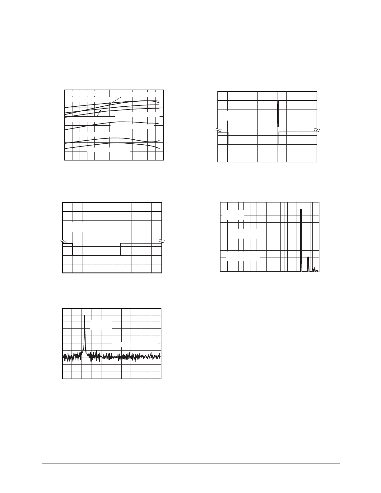
ILC6363 PRODUCT SPECIFICATION
Typical Performance Characteristics ILC6363CIR-ADJ
Unless otherwise specified: TA = 25°C, CIN = 100µF, C
V
vs Temperature
OUT
3.7
V
=3.6V (nominal)
OUT
VIN=4.2V, I
LOAD
=200mA
VIN=2.8V, I
LOAD
=200mA
3.6
(V)
3.5
OUT
V
VIN=3.6V, I
VIN=3.0V, I
LOAD
=200mA
LOAD
VIN=4.2V, I
VIN=4.2V, I
=500mA
LOAD
LOAD
=500mA
=500mA
3.4
3.3
-40-30-20
VIN=2.8V, I
-100102030405060708090
LOAD
=500mA
Temperature °C
< V
Low Battery Output (V
IN
for Less than 100ms)
TH
10kΩ pull-up resistor from LBO to 3V supply
4
3
2
VIN=1.2V
I
=40mA
1
OUT
LBO (V)
0
1.5
1.0
(V)
IN
V
0.5
0
20ms/div→
= 100µF, L = 15µH, V
OUT
Low Battery Output (V
10kΩ pull-up resistor from LBO to 3V supply
4
3
2
1
LBO (V)
0
1.5
1.0
(V)
IN
V
0.5
0
3.00
2.40
I
1.80
1.20
0.60
Output Noise Voltage (mVrms)
0
100 1k 10k 100k 1M
OUT
VIN=1.2V
I
=40mA
OUT
Spectral Noise Plot
VIN=2.8V
=68mA
OUT
Fundamental:
345kHz/2.7mVrms
First Harmonic
690kHz/0.66mVrms
= 3.6V (nominal)
< V
IN
for Greater than 100ms)
TH
20ms/div→
Freq (Hz)
Spectral Noise Plot
-42
-62
VIN=2.8V
I
OUT
=66mA
-82
-102
345kHz IF Band:2.6µVrms
-122
Output Noise Voltage (dBVrms)
-142
255k 335k 415k 495k 575k 655k
Freq (Hz)
12 REV. 1.3.5 5/21/02
Page 13
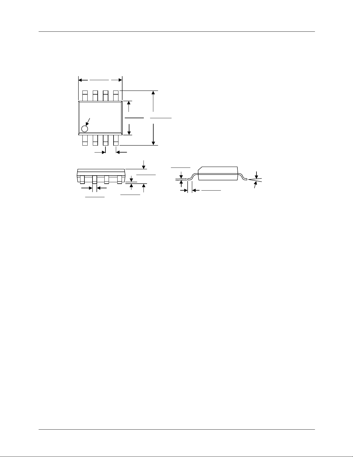
PRODUCT SPECIFICATION ILC6363
Mechanical Dimensions
8 Lead MSOP
0.122 (3.1)
0.114 (2.9)
Pin 1 identifier
0.016 (.40)
0.01 (.25)
0.122 (3.1)
0.114 (2.9)
0.025 (.65)BSC
0.043 (1.1)
0.031 (.80)
0.006 (.15)
0.004 (.05)
0.244 (5.15)
0.228 (4.65)
0.009 (.23)
0.005 (.13)
0.027 (.70)
0.016 (.40)
(0-10)°
REV. 1.3.5 5/21/02 13
Page 14

ILC6363 PRODUCT SPECIFICATION
Ordering Information for Ta = -40°C to +85°C, MSOP-8 Package
Part Number Output Voltage
ILC6363CIR50X 5.0
ILC6363CIRADJX Adjustable
DISCLAIMER
FAIRCHILD SEMICONDUCTOR RESERVES THE RIGHT TO MAKE CHANGES WITHOUT FURTHER NOTICE TO
ANY PRODUCTS HEREIN TO IMPROVE RELIABILITY, FUNCTION OR DESIGN. FAIRCHILD DOES NOT ASSUME
ANY LIABILITY ARISING OUT OF THE APPLICATION OR USE OF ANY PRODUCT OR CIRCUIT DESCRIBED HEREIN;
NEITHER DOES IT CONVEY ANY LICENSE UNDER ITS PATENT RIGHTS, NOR THE RIGHTS OF OTHERS.
LIFE SUPPORT POLICY
FAIRCHILD’S PRODUCTS ARE NOT AUTHORIZED FOR USE AS CRITICAL COMPONENTS IN LIFE SUPPORT DEVICES
OR SYSTEMS WITHOUT THE EXPRESS WRITTEN APPROVAL OF THE PRESIDENT OF FAIRCHILD SEMICONDUCTOR
CORPORATION. As used herein:
1. Life support devices or systems are devices or systems
which, (a) are intended for surgical implant into the body,
or (b) support or sustain life, and (c) whose failure to
perform when properly used in accordance with
2. A critical component in any component of a life support
device or system whose failure to perform can be
reasonably expected to cause the failure of the life support
device or system, or to affect its safety or effectiveness.
instructions for use provided in the labeling, can be
reasonably expected to result in a significant injury of the
user.
www.fairchildsemi.com
5/21/02 0.0m 003
2002 Fairchild Semiconductor Corporation
Stock#DS30006363
 Loading...