

Page 1
TECHNICAL DATA
1
INTEGRAL
2 x 1 W portable/mains-fed stereo
power amplifier
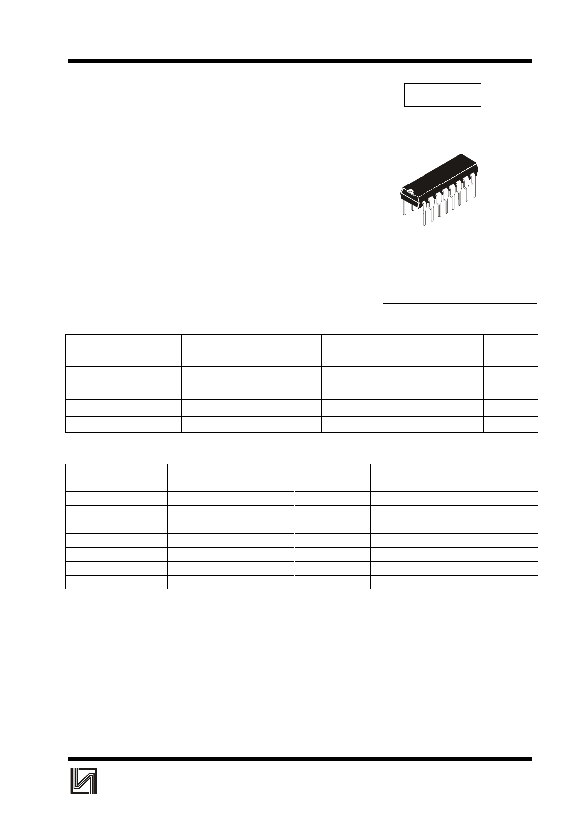
The ILA7053N is an integrated class-B stereo power amplifier in a 16-lead
dual-in-line (DIL) plastic package. The device, consisting of two BTL
amplifiers, is primarily developed for portable audio applications but may
also be used in mains-fed applications.
• No external components
• No switch-ON/OFF clicks
• Good overall stability
• Low power consumption
• Short-circuit-proof
QUICK REFERENCE DATA
PARAMETER CONDITIONS SYMBOL MIN. MAX. UNIT
Supply voltage range V
P
318V
Total quiescent current
R
L
= ∞
I
tot
-16mA
Output power
R
L
= 8 Ω, V
P
= 6 V, THD = 10%
P
O
-1W
Internal voltage gain
R
L
= 8 Ω, V
P
= 6 V
Gv 38 40 dB
Total harmonic distortion
P
O
= 0.1 W, R
L
= 8 Ω, V
P
= 6 V
THD - 1.0 %
PINNING
Pin № Symbol Description Pin № Symbol Description
01 SGND1 signal ground 1 09 OUT2A output 2 (positive)
02 IN1 input 1 10 GND2 power ground 2
03 n.c. not connected 11 n.c. not connected
04 n.c. not connected 12 OUT2B output 2 (negative)
05 V
P
supply voltage 13 OUT1B output 1 (negative)
06 IN2 input 2 14 GND1 power ground 1
07 SGND2 signal ground 2 15 n.c. not connected
08 n.c. not connected 16 OUT1A output 1 (positive)
Note
The information contained within the parentheses refer to the polarity of the loudspeaker terminal to which the
output must be connected.
FUNCTIONAL DESCRIPTION
The ILA7053N is a stereo output amplifier, with an internal gain of 39 dB, which is primarily for use in portable
audio applications but may also be used in mains-fed applications. The current trends in portable audio application
design is to reduce the number of batteries which results in a reduction of output power when using conventional
output stages.
The ILA7053N overcomes this problem by using the Bridge-Tied-Load (BTL) principle and is capable of delivering
1.2 W into an 8 Ω load (V P = 6 V). The load can be short-circuited under all input conditions.
ILA7053N
N SUFFIX
1
16
ORDERING INFORMATION
ILA7053N Plastic DIP
T
A
= -25 ° to +70° C
Page 2
ILA7053N
2
INTEGRAL
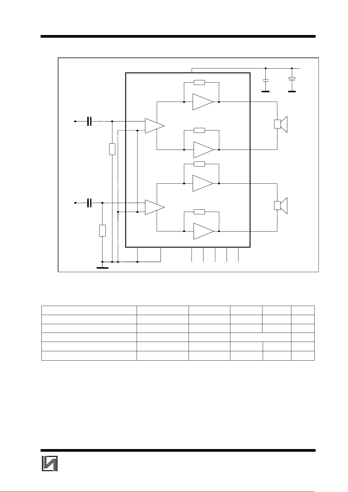
Fig.1 Block diagram, test and application circuit diagram
RATINGS
Limiting values in accordance with the Absolute Maximum System
PARAMETER CONDITIONS SYMBOL MIN. MAX. UNIT
Supply voltage V
P
-18V
Non-repetitive peak output current I
OSM
-1.5A
Total power dissipation P
tot
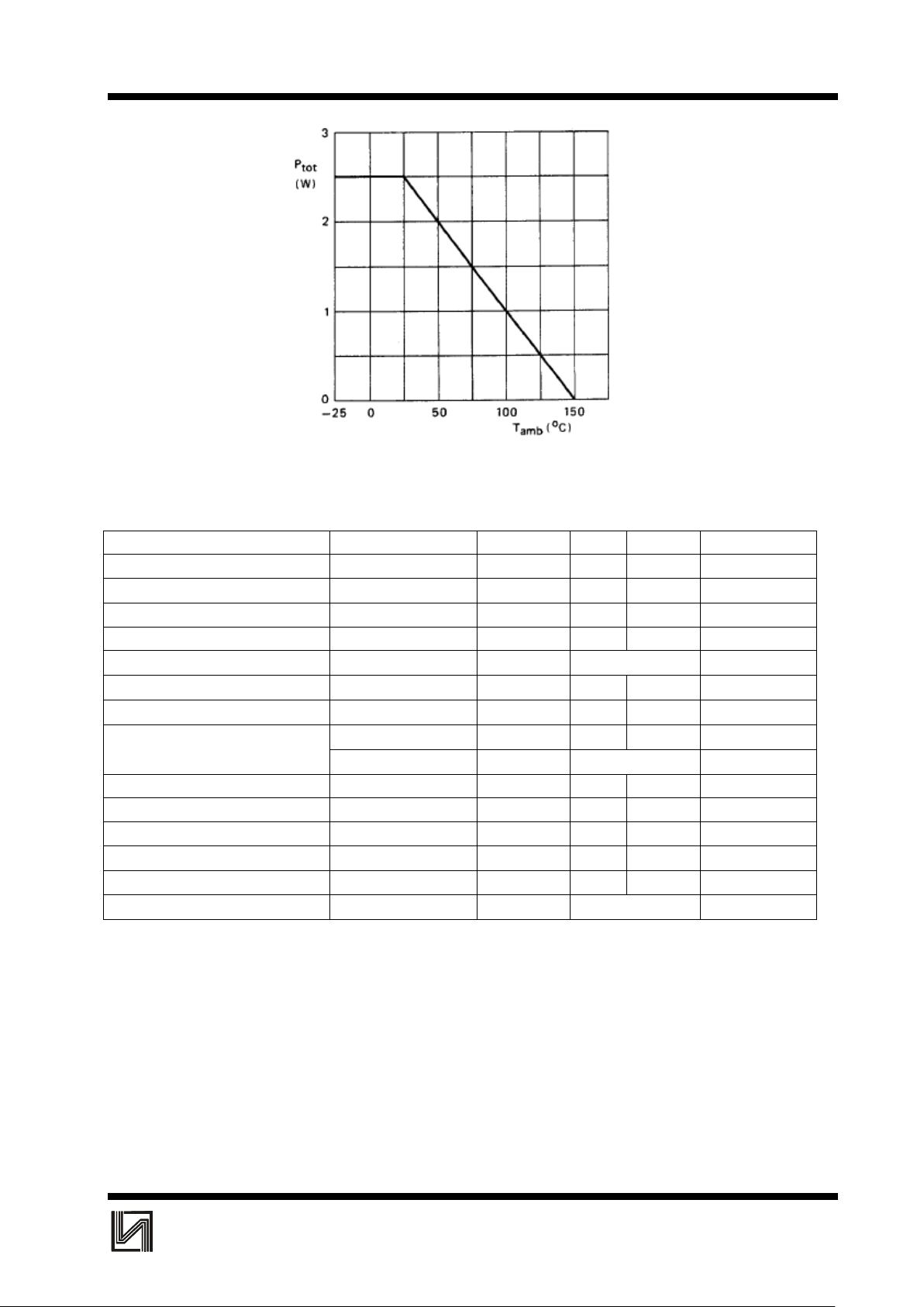
see Fig.2
Crystal temperature Tc - +150
°C
Storage temperature range Tstg -60 +150
°C
THERMAL RESISTANCE
From junction to ambient R
th j-a
60 K/W
Power dissipation
Assuming: VP = 6 V and R
L
= 8 Ω:
The maximum sinewave dissipation is 1.8 W, therefore T
amb(max.)
= 150 - (60 x 1.8) = 42°C.
05
02
01
16
13
+Vp
Rs=5,1
k
ΩΩΩΩ
RL
1
0,1
µµµµ
F
220,0
µµµµ
F
+
-
+
_
Cin=(0, 47 -1 0,0)
µµµµ
F
S
G
N
D
1
06
07
10
12
09
Rs=5,1
k
ΩΩΩΩ
RL
2
GND-2
S
G
N
D
2
14
GND-1
ILA7053N
11 150803 04
Vi2
Vi1
Cin=(0, 47 -1 0,0)
µµµµ
F
-
+
Page 3
ILA7053N
3
INTEGRAL
Fig.2 Power derating curve
CHARACTERISTICS
VP = 6 V; RL = 8 W; Tamb = 25°C; unless otherwise specified; measured from test circuit, Fig.2.
PARAMETER CONDITIONS SYMBOL MIN. MAX. UNIT
Supply voltage range V
P
318 V
Total quiescent current
R
L
= ∞; note 1
I
tot
-16 mA
Input bias current I
bias
- 300 nA
Supply voltage ripple rejection note 2 SVRR 40 - dB
Input impedance Z
I
100 (type)
kΩ
DC output offset voltage note 3
∆V
13-16
- 100 mV
∆V
12-9
- 100 mV
note 4 V
no(rms)
- 300
µV
Noise output voltage
(RMS value)
note 5 V
no(rms)
60 (type)
µV
Output power THD = 10% PO 0.8 W
Total harmonic distortion PO = 0.1 W THD - 1.0 %
Internal voltage gain G
V
38 40 dB
Channel balance
∆G
V
-1 dB
Channel separation note 3
α
40 - dB
Frequency response
R
L
= 8 Ω, V
P
= 6 V
f 0.02 to 20 (type) kHz
Notes to the characteristics
1. With a practical load the total quiescent current depends on the offset voltage.
2. Ripple rejection measured at the output with R
S
= 0 Ω and f = 100 Hz to 10 kHz. The ripple voltage (200 mV) is
applied to the positive supply rail.
3. R
S
= 5 kΩ.
4. The noise output voltage (RMS value) is measured with R
S
= 5 kΩ, unweighted and a bandwidth of 60 Hz to 15
kHz.
5. The noise output voltage (RMS value) is measured with R
S
= 0 Ω and f = 500 kHz with 5 kHz bandwidth. If R
L
=
8 Ω and L
L
= 200 mH the noise output current is only 100 nA.
Page 4
ILA7053N
4
INTEGRAL
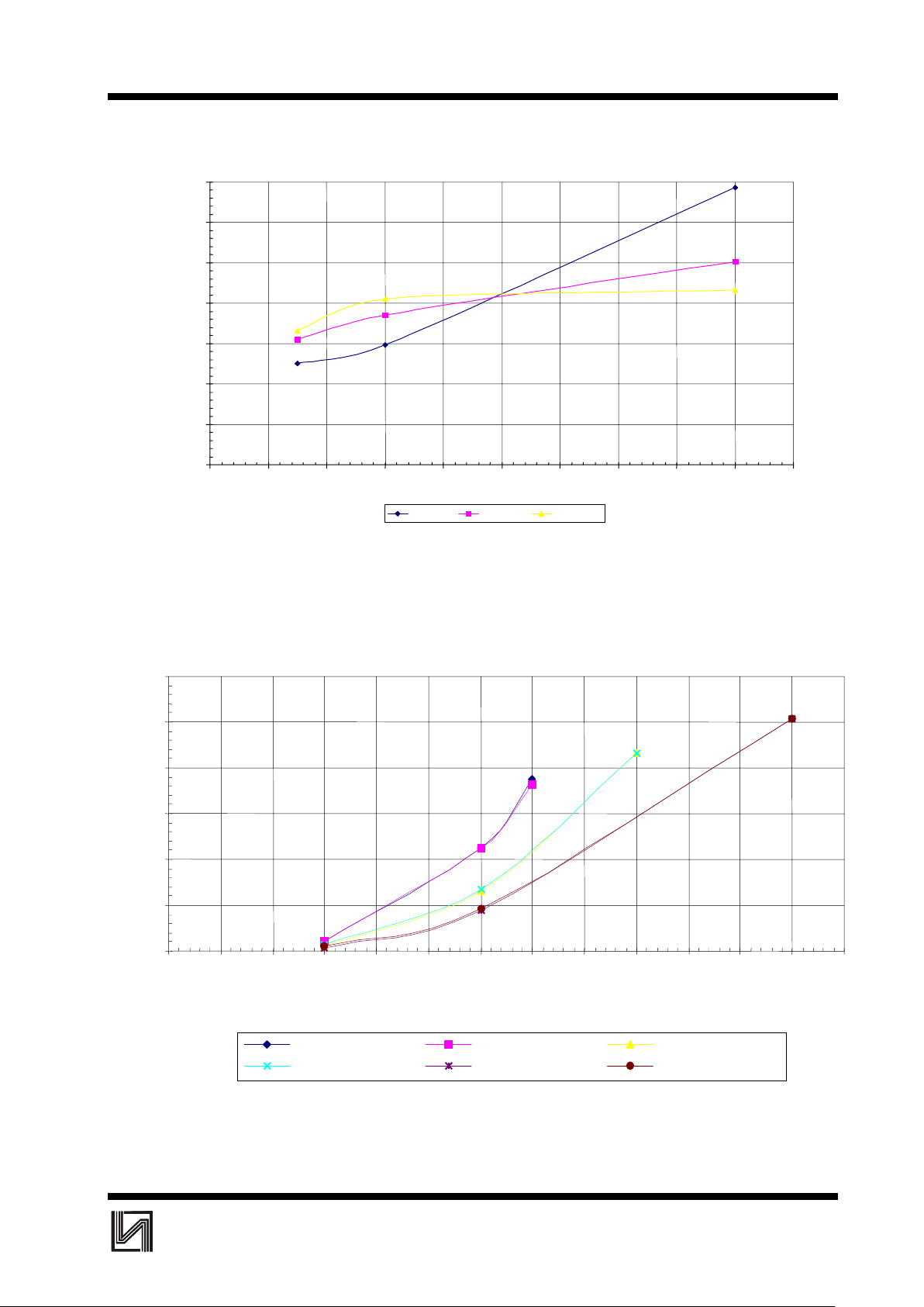
Fig.3. Output power as a function of voltage supply (V P ); THD = 10%; f = 1 kHz; T amb = 60 ºC.
Fig.4. Output power as a function of voltage supply (V
P
); THD = 10%; f = 1 kHz; T amb = 60 ºC.
0,0
2,0
4,0
6,0
8,0
10,0
12,0
14,0
0,0 2,0 4,0 6,0 8,0 10,0 12,0 14,0 16,0 18,0
Vp, V
Ip, mA
Ta=-25 °C, Ta=25 °C, Ta=70 °C,
T= -25
°°°°
C
T= 25
°°°°
C
T=70
°°°°
C
0,000
0,500
1,000
1,500
2,000
2,500
3,000
0,0 1,0 2,0 3,0 4,0 5,0 6,0 7,0 8,0 9,0 10,0 11,0 12,0 13,0
Vp (V)
Po (W)
Ta=+25 C, RL= 8 Ω Ta=+60 C, RL= 8 Ω Ta=+25 C, RL= 16 Ω
Ta=+60 C, RL= 16 Ω Ta=+25 C, RL= 25 Ω Ta=+60 C, RL= 25 Ω
Ta=+25 C, RL=8 Ω
Ta=+25 C, RL+16 Ω
Ta=+60 C, RL=16 Ω
Ta=+25 C, RL=25 Ω
Ta=+60 C, RL=25 Ω
Ta=+60 C, RL=8 Ω
Page 5
ILA7053N
5
INTEGRAL
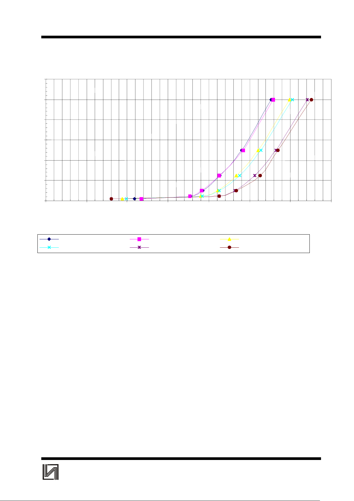
Fig.5 Total harmonic distortion as a function of output power; f = 1 kHz; T amb = 60 ºC.
0,0
2,0
4,0
6,0
8,0
10,0
12,0
0,000 0,200 0,400 0,600 0,800 1,000 1,200 1,400
Po (W)
THD (%)
Ta=+25C, Up=6,0V, RL=8 Ω, Ta=+60C, Up=6,0V, RL=8 Ω, Ta=+25C, Up=7,5V, RL=16 Ω,
Ta=+60C, Up=7,5V, RL=16 Ω, Ta=+25C, Up=9,0V, RL=25 Ω, Ta=+60C, Up=9,0V, RL=25 Ω,
Page 6
ILA7053N
6
INTEGRAL
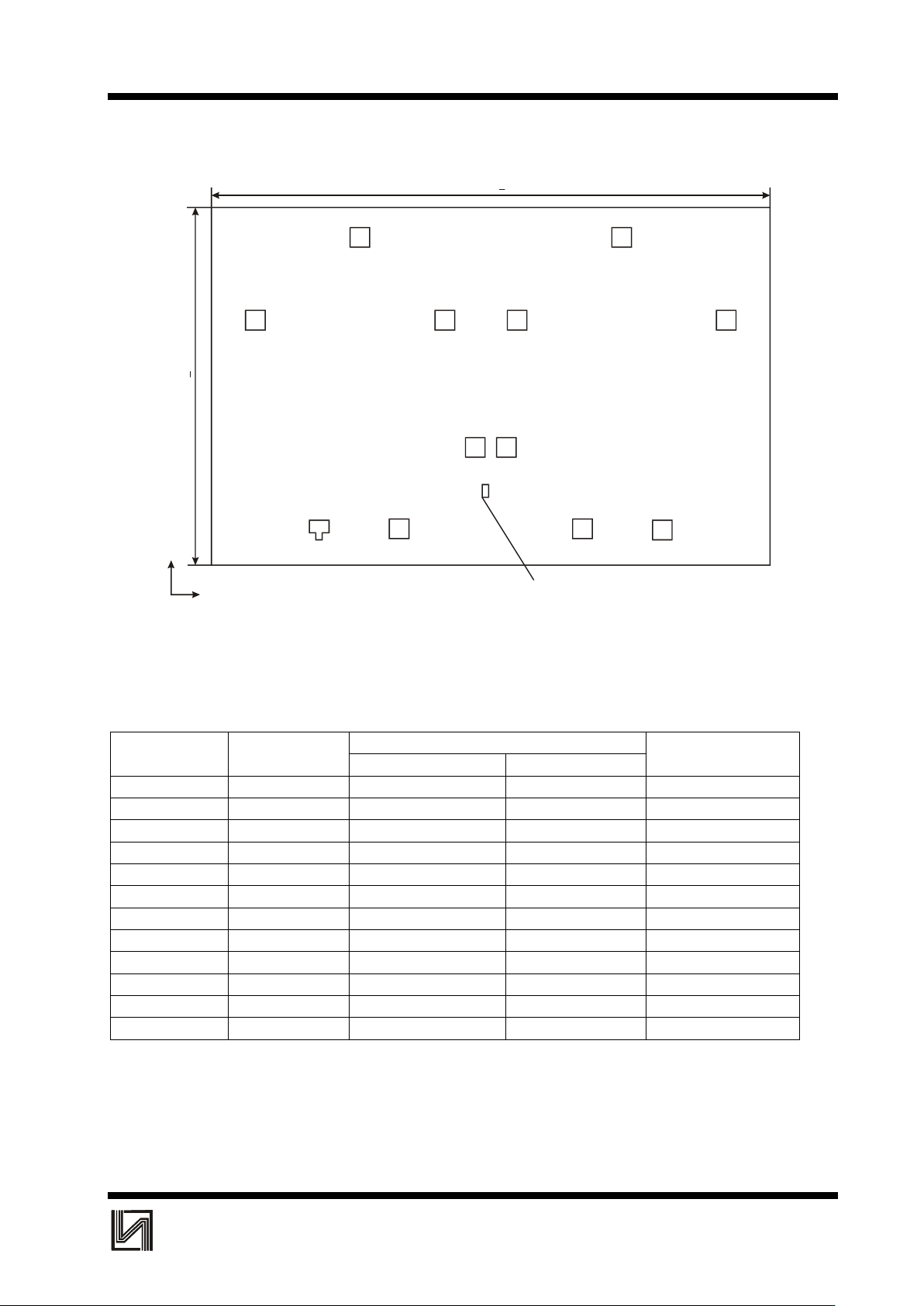
CHIP PAD DIAGRAM
Location of marking (mm): left lower corner x=1.657, y=0.415.
Chip thickness: 0.35 ± 0.02 mm.
PAD LOCATION
Location (left lower corner), mm
Pad No Symbol
XY
Pad size, mm
01 SGND1 0.600 0.155 0.120 x 0.120
02 IN1 1.089 0.162 0.120 x 0.120
03 V
P
1.555 0.661 0.120 x 0.120
04 V
P
1.745 0.661 0.120 x 0.120
05 IN2 2.211 0.162 0.120 x 0.120
06 SGND2 2.700 0.155 0.120 x 0.120
07 OUT2A 3.091 1.440 0.120 x 0.120
08 GND2 2.451 1.947 0.120 x 0.120
09 OUT2B 1.811 1.440 0.120 x 0.120
10 OUT1B 1.489 1.440 0.120 x 0.120
11 GND1 0.849 1.947 0.120 x 0.120
12 OUT1A 0.209 1.440 0.120 x 0.120
Note: Pad location is given as per passivation layer
01
02
03
04
05
06
07
08
09
10
11
12
3.42 + 0.03
2.19 + 0.03
Chip marking
710
(0,0)
X
Y
 Loading...