

Page 1
ILA7056SH
1
INTEGRAL
3 W Mono BTL Audio Output Amplifier
FEATURES
· No external components
· No switch-on/off clicks
· Good overall stability
· Low power consumption
· Short circuit proof
· ESD protected on all pins.
GENERAL DESCRIPTION
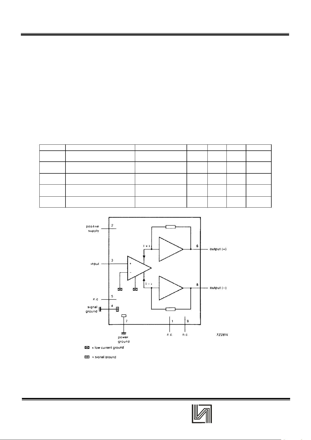
The ILA7056SH is a mono output amplifier contained in a
9 pin SIL medium power package (SOT110).
The device is designed for battery-fed portable mono
recorders, radios and television.
QUICK REFERENCE DATA
SYMBOL PARAMETER CONDITIONS MIN. TYP. MAX. UNIT
Vp
supply voltage 3 11 18 V
Po
output power
Vp=11 V, THD=10!,
RL=16 "
2.5 3 W
Gv
internal voltage gain 39 40,0 42 dB
Ip
total quiescent current
Vp=11 V; RL=#
57mA
THD
total harmonic distortion Po=0,5 W 0,25 1 %
Page 2
ILA7056SH
2
INTEGRAL
PIN DESCRIPTION
1n.c.
2VP
3 input(+)
4 signal ground
5n.c.
6 output(+)
7 power ground
8 output(-)
9n.c.
FUNCTIONAL DESCRIPTION
The ILA7056SH is a mono output amplifier, designed for battery-fed portable radios and mains-fed equipment such as
television. For space reasons there is a trend to decrease the number of external components. For portable applications there
is also a trend to decrease the number of battery cells, but still a reasonable output power is required.
The ILA7056SH fulfills both of these requirements. It needs no peripheral components, because it makes use of the BridgeTied-Load (BTL) principle. Consequently it has, at the same supply voltage, a higher output power compared to a conventional
Single Ended output stage. It delivers an output power of 1 W into a loudspeaker load of 8 W with 6 V supply or 3 W into 16 W
loudspeaker at 11 V without need of an external heatsink. The gain is internally fixed at 40 dB. Special attention is given to
switch-on/off click suppression, and it has a good overall stability. The load can be short circuited at all input conditions.
SYMBOL PARAMETER CONDITIONS MIN. MAX. UNIT
Vp supply voltage - 18 V
iorm Peak output current repetitive - 1 A
iosm Peak output current non-repetitive - 1.5 A
Tstg storage temperature range -55 150 °C
Tj junction temperature - 150 °C
Plot total power dissipation T^se < 60 •••C - 9 W
Tsc short circuiting time see note 1 - 1 hr
Note
1. The load can be short-circuited at all input conditions.
SYMBOL PARAMETER NOM. UNIT
hibk from junction to case 10 K/W
Rtll.a from junction to ambient in free air 55 K/W
POWER DISSIPATION
Assume: VP = 11 V; RL = 16 W.
The maximum sine-wave dissipation is 1.52 W.
The Rth j-a of the package is 55 K/W.
Tamb max = 150 - 55 ´ 1.52 = 66.4 °C.
Page 3
ILA7056SH
3
INTEGRAL
CHARACTERISTICS
SYMBOL PARAMETER CONDITIONS MIN. TYP. MAX. UNIT
Vp operating supply voltage 3 11 18 V
IQRM
repetitive peak output current - - 0.6 A
IP
total quiescent current - 5 7 mA
PO
output power THD= 10% 2.5 3 - W
THD total harmonic distortion Po = 0.5 W - 0.25 1
GV
voltage gain 39 40.5 42 dB
Vno noise output voltage note 2 - 180 300 uV
Vno noise output voltage note 3 - 60 - [JV
frequency response - 20 to
20.000
-Hz
RR ripple rejection note 4 36 50 - dB
AV DC-output offset voltage note 5 - - 200 mV
IZJ input impedance - 100 - kii
1, input bias current - 100 300 nA
Notes to the characteristics
1. With a load connected to the outputs the quiescent current will increase, the maximum value of this increase being equal to
the DC output offset voltage divided by RL .
2. The noise output voltage (RMS value) is measured with RS = 5 kW unweighted (20 Hz to 20 kHz).
3. The noise output voltage (RMS value) at f = 500 kHz is measured with RS = 0 W and bandwidth = 5 kHz. With a practical
load (RL = 16 W, LL = 200 mH) the noise output current is only 50 nA.
4. The ripple rejection is measured with RS = 0 W and f = 100 Hz to 10 kHz. The ripple voltage (200 mV) is applied to the
positive supply rail.
5. RS = 5 kW.
 Loading...