

Page 1

GL811USB -
Genesys Logic, Inc.
USB 2.0 to ATA / ATAPI Bridge
Controller
Specification 1.3
May 10, 2002
Genesys Logic, Inc.
10F, No.11, Ln.155, Sec.3, Peishen Rd., Shenkeng, Taipei, Taiwan
Tel: 886-2-2664-6655 Fax: 886-2-2664-5757
http://www.genesyslogic.com
Page 2

GL811USB – USB 2.0 to ATA / ATAPI Bridge Controller
Contents
1. General Description.........................................................................................2
2. Features............................................................................................................3
3. Function Block.................................................................................................4
3.1 Block Diagram..............................................................................................4
3.2 Functional Overview.....................................................................................5
4. Pinning Information.........................................................................................7
4.1 Pin Assignment.............................................................................................7
4.2 Pin Description .............................................................................................8
5. Functional Description..................................................................................10
5.1 A TA/ ATAPI .................................................................................................10
5.2 USB 2.0......................................................................................................10
6. Electrical Characteristics..............................................................................11
6.1 Absolute Maximum Ratings........................................................................ 11
6.2 Temperature Conditions .............................................................................11
6.3 DC Characteristics...................................................................................... 11
6.4 AC Characteristics- ATA/ ATAPI..................................................................13
6.5 AC Characteristics- USB 2.0 ......................................................................33
7. Package Dimension.......................................................................................34
8. Revision History.............................................................................................35
©2000-2002 Genesys Logic Inc.—All rights reserved. Page 1
Page 3

GL811USB – USB 2.0 to ATA / ATAPI Bridge Controller
1. General Description
The GL811USB is a highly-compatible, low cost USB 2.0 to ATA / ATAPI bridge
controller, which integrates Genesys Logic own design high speed UTMI (USB 2.0
Transceiver Macrocell Interface) transceiver.
As a one-chip solution which complies with Universal Serial Bus specification rev.
2.0 and ATA / ATAPI-6 specification rev 1.0, the GL811USB can support various
kinds of ATA / ATAPI device. There are totally 4 endpoints in the GL811USB
controller, Control (0), Bulk In (1), Bulk Out (2), and Interrupt (3). By complies with
the USB Storage Class specification ver.1.0 (Bulk only protocol), the GL811USB
can support not only plug and play but also Windows XP/ 2000/ ME default driver.
The GL811USB uses 12MHz crystal and slew-rate controlled pads to reduce the
EMI issue. With 48-pin LQFP (9mmX9mm) package, the GL811USB is the best
cost/ performance solution to fit different situations in the USB 2.0 high speed
storage class applications such as Hard Disk, CD-ROM, CD-R / RW and
DVD-ROM.
©2000-2002 Genesys Logic Inc.—All rights reserved. Page 2
Page 4

GL811USB – USB 2.0 to ATA / ATAPI Bridge Controller
2. Features
Complies with Universal Serial Bus specification rev. 2.0.
Complies with ATA/ATAPI-6 specification rev 1.0.
Complies with USB Storage Class specification ver.1.0. (Bulk only protocol)
Operating system supported: Win XP/ 2000/ ME/ 98/ 98SE; Mac OS 9.X/ X.
Supports 4 endpoints: Control (0) / Bulk Read (1) / Bulk Write (2) / Interrupt
(3).
64 / 512 bytes Data Payload for full / high speed Bulk Endpoint.
Supports 8-bit/16-bit Standard PIO mode interface.
Supports 16-bit Multiword DMA mode and Ultra DMA mode interface (Ultra 33
/ 66 / 100).
Embedded USB 2.0 UTMI transceiver.
Embedded 7.5 MIPS RISC CPU.
ROM size: 4k words; RAM size: 128 bytes.
Supports Power Down mode and USB suspend indicator.
Supports USB 2.0 TEST mode features.
12MHz external clock to provide better EMI3.3V power input.
5V tolerance pad for IDE interface.
Supports Wakeup ability.
Available in 48-pin LQFP (9 mm * 9mm) package.
©2000-2002 Genesys Logic Inc.—All rights reserved. Page 3
Page 5
C
GL811USB – USB 2.0 to ATA / ATAPI Bridge Controller
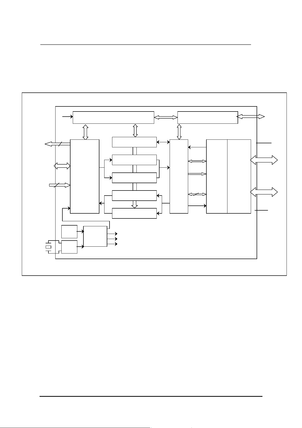
3. Function Block
3.1 Block Diagram
DMACK_
DIOR_
DIOW_
CS1_,
CS0_
DA2
DA1
DA0
IODD15-0
INTRQ
CBLID_
DMARQ
IORDY
LK15
8
8/16-Bit
4
12-96MHz
Engine
IDE
CPU
Control Register
CLK30
RXSTS
SIE
TXCTL
16
DATA
UTMI
LOGIC
USB2.0
TXCVR
GPIO1
GPIO7
RPU
DPF
DPH
DMF
DMH
12MHz
X10
X40
RREF
Clkgen
©2000-2002 Genesys Logic Inc.—All rights reserved. Page 4
Page 6

GL811USB – USB 2.0 to ATA / ATAPI Bridge Controller
3.2 Functional Overview
3.2.1 USB 2.0 TXCVR
The USB 2.0 Transceiver is the analog circuitry to handle the USB HS/FS
signaling.
3.2.2 UTMI (USB 2.0 Transceiver Macrocell Interface) Logic
The UTMI Logic is compliant to Intel’s UTMI specification 1.01. This block handles
the low level USB protocol and signaling. The major jobs of UTMI Logic is data and
clock recovery, NRZI encoding/decoding, Bit Stuffing/De-stuffing, USB2.0 test
modes supporting and serial / parallel conversion.
3.2.3 SIE (Serial Interface Engine)
The SIE contains the USB packet ID and address recognition logic, and other
sequencing and state machine logic to handle USB packets and transactions.
3.2.4 PLL
10XPLL provides the 120MHz clock output for UTMI Logic block. UTMI operates in
120MHz for USB HS data processing. 40XPLL block will provide 480MHz for USB
HS data transmission.
3.2.5 CLKGEN
CLKGEN is the clock generator block for the logic blocks. It generates 15MHz
clock for micro controller, 12MHz for PIO mode, 48MHz for MDMA mode, 96MHz
for UDMA mode, and 30MHz clock for UTMI, SIE, and FIFO.
3.2.6 CPU
The CPU is the control center of GL811USB. It’s an 8-bit micro controller operating
in 15MHz, 7.5 MIPS. After receiving a USB command, it decodes the host
command, then it re-assigns tasks to the IDE engine, GPIO, FIFO, and response
proper data/status to USB host.
3.2.7 IDE Engine
The IDE engine is extended from standard ATA / ATAPI protocol. It supports PIO
mode, multiword DMA mode, and ultra DMA mode data transfers.
©2000-2002 Genesys Logic Inc.—All rights reserved. Page 5
Page 7

GL811USB – USB 2.0 to ATA / ATAPI Bridge Controller
3.2.8 FIFOs
Control FIFO is used as Control Read / Write FIFO. TXFIFO0 / TXFIFO1 are two
sets of 512-byte ping-pong FIFO for Bulk Read endpoint. It buffers data from IDE
engine, and re-direct to USB SIE logic. RXFIFO0 / RXFIFO1 are two sets of
512-byte ping-pong FIFO for Bulk Write endpoint. It buffers data from USB SIE
logic, and re-direct to IDE engine.
3.2.9 Control Registers
Control Register configures GL811USB to proper operation. For example, CPU
can set register to generate wakeup event, enter suspend, transmits proper USB
packet to host.
©2000-2002 Genesys Logic Inc.—All rights reserved. Page 6
Page 8
_
A
_
K
GL811USB – USB 2.0 to ATA / ATAPI Bridge Controller
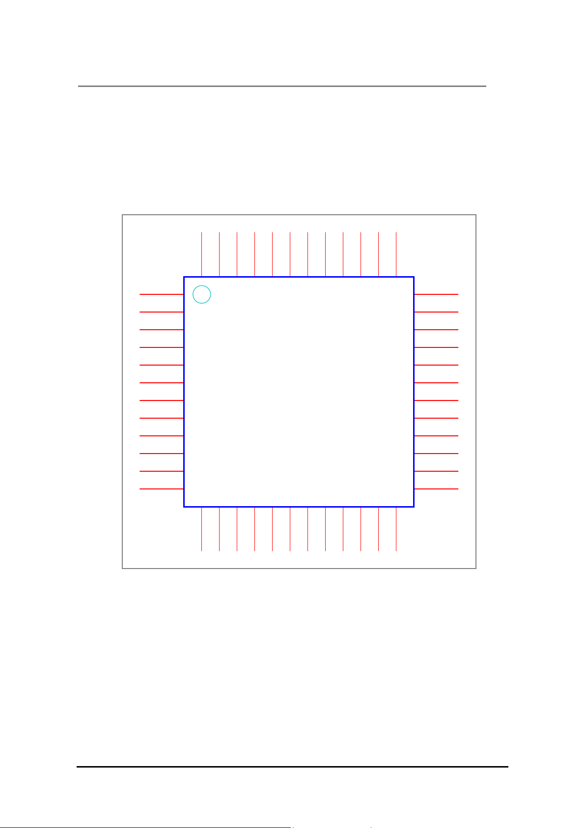
4. Pinning Information
4.1 Pin Assignment
GPIO1
IODD[7]
IODD[6]
IODD[5]
IODD[4]
DVCC2
DGND2
IODD[3]
IODD[2]
IODD[1]
IODD[0]
38
23
DMARQ
37
36
35
34
33
32
31
30
29
28
27
26
25
24
DIOW_
DIOR_
IORDY
DMACK_
INTRQ
DA1
DA0
CS0_
TEST
GND1
X1
X2
IODD[10]
IODD[11]
IODD[12]
IODD[13]
IODD[14]
IODD[15]
GPIO7
IODD[8]
IODD[9]
DVCC1
DGND1
CBLID
1
2
3
4
5
6
7
8
9
10
11
12
48
47
46
45
44
43
42
41
40
39
GL811USB
48 LQFP
13
14
15
16
17
18
19
20
21
22
CS1
DA2/ S
RPU
RESET#
AVCC0
DPF
DPH
DMF
DMH
RREF
AGND0
AVCC1
©2000-2002 Genesys Logic Inc.—All rights reserved. Page 7
Page 9
GL811USB – USB 2.0 to ATA / ATAPI Bridge Controller
4.2 Pin Description
Pin # Name I/O Pad Type Description Note
1
2~5
6
7
8~11
12
13
14
15
16
17
18
19
20
21
22
23
24
25
26
27
28
29
30
31
32
33
34
35
36
37
GPIO7
IODD [8:11]
DVCC1
DGND1
IODD [12:15]
CBLID_
CS1_
DA2
RESET#
RPU
AVCC0
DPF
DPH
DMF
DMH
AGND0
RREF
AVCC1
X2
X1
AGND1
TEST
CS0_
DA0
DA1
INTRQ
DMACK_
IORDY
DIOR_
DIOW_
DMARQ
B
I/O 8(*) GPIO7 (**)
B I/O 16(*) IDE data bus 8~11
tri
tri
P Power Digital VCC
P Power Digital ground
B I/O 16 IDE data bus 12~15
I I/O 8 Cable select input
O I/O 16 Chip select 1
O I/O 16 IDE address 2
I I/O 8 Reset pin (***)
tri
tri
tri
tri
pu
A U20mia 3.3v output
P Power Analog VCC
B U20mia Full speed DP
B U20mia High speed DP
B U20mia Full speed DM
B U20mia High speed DM
P Power Analog ground
A U20mia Reference resister connect (****)
P Power Analog VCC
B Clock Crystal output
I Clock Crystal input, 12Mhz
P Power Analog ground
I I/O 8 TEST mode input
O I/O 16 Chip select 0
O I/O 16 IDE address 0
O I/O 16 IDE address 1
I I/O 8 IDE interrupt input
O I/O 16 IDE acknowledge
I I/O 16 IDE ready
O I/O 16 IDE read signal
O I/O 16 IDE write signal
I I/O 8 IDE request
pd
tri
tri
tri
tri
tri
pu
tri
tri
pd
©2000-2002 Genesys Logic Inc.—All rights reserved. Page 8
Page 10

4
GL811USB – USB 2.0 to ATA / ATAPI Bridge Controller
Pin # Name I/O Pad Type Description Note
38~41
42
43
4~47
48
IODD[0:3]
DGND2
DVCC2
IODD[4:7]
GPIO1
B I/O 16 IDE data bus 0~3
P Power Digital ground
P Power Digital VCC
B I/O 16 IDE data bus 4~7
B I/O 8 GPIO1
tri
tri
pd
(*) The different of I/O 8 type from I/O 16 type is the typical drive current. The typical drive
current of I/O 8 type is 8 mA, and for I/O pad 16 is 16 mA.
(**) When operating in default mode: GPIO7 is the ATA/ ATAPI reset input,
(***) When Reset pin is pulled low, the IDE bus will be in tri-state.
(****) RREF must be connected with a 510 ohm resister to ground.
Notation:
Description
Note
O Output
I Input
B Bi-directional
P Power
A Analog
pu Internal pull up
pd Internal pull down
tri Tri-state
©2000-2002 Genesys Logic Inc.—All rights reserved. Page 9
Page 11

GL811USB – USB 2.0 to ATA / ATAPI Bridge Controller
5. Functional Description
5.1 ATA/ ATAPI
The GL811USB complies with ATA/ATAPI-6 specification rev. 1.0. Please refer to the
specifications for more information.
5.2 USB 2.0
The GL811USB complies with Universal Serial Bus specification rev. 2.0, and it
integrates Genesys Logic own design UTMI transceiver that fully complies with the
USB 2.0 Transceiver Macercell Interface (UTMI) specification rev. 1.01. Please refer
to the specifications for more information.
©2000-2002 Genesys Logic Inc.—All rights reserved. Page 10
Page 12

GL811USB – USB 2.0 to ATA / ATAPI Bridge Controller
6. Electrical Characteristics
6.1 Absolute Maximum Ratings
Symbol Description Min Max Unit
VCC DC supply voltage +3.0 +3.6 V
VI DC input voltage -0.3 V
V
DC input voltage range for I/O -0.3 V
I/O
V
DC input voltage for USB D+/D- pins -0.3 V
AI/O
V
Static discharge voltage 4000 V
ESD
TA Ambient Temperature 0 100
6.2 Temperature Conditions
Item Value
Storage Temperature -50oC ~ 150 oC
Operating Temperature 0 oC ~ 70 oC
6.3 DC Characteristics
+ 0.3 V
CC
+ 0.3 V
CC
+ 0.3 V
CC
o
C
6.3.1 I/O 8 Type digital pins (For pad type I/O 8 @ V
=3.6V)
CC
Parameter Min Typ Max Unit
Current sink @ VOL = 0.4V 7.79 10.83 14.09 mA
Current output @ V
= 2.4V (TTL high) 16.36 19.87 23.39 mA
OH
Falling slew rate at 30 pF loading capacitance 0.26 0.50 0.80 V/ns
Rising slew rate at 30 pF loading capacitance 0.30 0.57 0.91 V/ns
Input high threshold voltage 1.64 V
Input low threshold voltage 1.36 V
©2000-2002 Genesys Logic Inc.—All rights reserved. Page 11
Page 13

GL811USB – USB 2.0 to ATA / ATAPI Bridge Controller
Parameter Min Typ Max Unit
Hysteresis voltage - 0 - V
Leakage current for pads with internal pull up or pull
down resistor
Pad internal pull down resister 51K 105K 152K Ohms
Pad internal pull up resister 85K 168K 251K Ohms
Supply current 109 mA
46
6.3.2 I/O 16 Type digital pins (For pad type I/O 16 @ V
Parameter Min Typ Max Unit
Current sink @ VOL = 0.4V 16.20 21.90 27.68 mA
Current output @ V
Falling slew rate at 30 pF loading capacitance 0.51 0.93 1.35 V/ns
Rising slew rate at 30 pF loading capacitance 0.46 0.83 1.27 V/ns
Input high threshold voltage 2.15 V
= 2.4V (TTL high) 24.13 29.46 34.80 mA
OH
=3.6V)
CC
µA
Input low threshold voltage 0.89 V
Pad internal pull down resister 51K 105K 152K Ohms
6.3.3 D+/ D- (For pad type u20mia @ V
=3.6V)
CC
Parameter Min Typ Max Unit
D+/D- static output LOW (RL of 1.5K to VCC ) 0 0.3 V
D+/D- static output HIGH (RL of 15K to GND ) 2.8 3.6 V
Differential input sensitivity 0.2 V
Single-ended receiver threshold 0.8 2.0 V
Transceiver capacitance 20 pF
Hi-Z state data line leakage -10 +10
Driver output resistance 28 43 Ohms
µA
©2000-2002 Genesys Logic Inc.—All rights reserved. Page 12
Page 14

GL811USB – USB 2.0 to ATA / ATAPI Bridge Controller
6.3.4 Switching Characteristics
Parameter Min Typ Max Unit
X1 crystal frequency 11.97 12 12.03 MHz
X1 cycle time 83.3 ns
D+/D- rise time with 50pF loading 4 20 ns
D+/D- fall time with 50pF loading 4 20 ns
6.4 AC Characteristics- ATA/ ATAPI
The GL811USB complies with ATA / ATAPI-6 specification rev 1.0, which supports
following data transfer modes:
1. PIO (Programmed Input/ Output) data transfer:
PIO data transfers are performed by the host processor utilizing PIO register
accesses to the Data register.
2. DMA (Direct Memory Access) data transfer:
DMA data transfer means of data transfer between device and host memory
without host processor intervention.
- Multiword DMA: Multiword DMA is a data transfer protocol used with the READ
DMA, WRITE DMA, READ DMA QUEUED, WRITE DMA QUEUED and
PACKET commands. When a Multiword DMA transfer is enabled as indicated by
IDENTIFY DEVICE or IDENTIFY PACKET DEVICE data, this data transfer
protocol shall be used for the data transfers associated with these commends.
(Please refer to the ATA / ATAPI-6 specification rev 1.0 for more information.)
- Ultra DMA: Ultra DMA Is a data transfer protocol used with the READ DMA,
WRITE DMA, READ DMA QUEUED, WRITE DMA QUEUED and PACKET
commands. When this protocol is enabled, the Ultra DMA protocol shall be used
instead of the Multiword DMA protocol when these commands are issued by the
host. This protocol applies to the Ultra DMA data burst only. (Please refer to the
ATA / ATAPI-6 specification rev 1.0 for more information.)
Following listed the symbols and their respective definitions that are used in the timing
diagram:
©2000-2002 Genesys Logic Inc.—All rights reserved. Page 13
Page 15

GL811USB – USB 2.0 to ATA / ATAPI Bridge Controller
- Signal transition (asserted or negated)
- Data transition (asserted or negated)
- Data valid
- Undefined but not necessarily released
- Asserted, negated or released
- Released
- The “other” condition if a signal is shown with no change
All signals are shown with the asserted condition facing to the top of the page. The
negated condition is shown towards the bottom of the page relative to the asserted
condition.
The interface uses a mixture of negative and positive signals for control and data. The
terms asserted and negated are used for consistency and are independent of
electrical characteristics.
In all timing diagrams, the lower line indicates negated, and the upper line indicates
asserted. The following illustrates the representation of a signal named Test going
from negated to asserted and back to negated, based on the polarity of the signal.
Test
Test_
> VIH
< V
IL
< VIL
> V
IH
Assert
Assert
Negate
Negate
©2000-2002 Genesys Logic Inc.—All rights reserved. Page 14
Page 16

GL811USB – USB 2.0 to ATA / ATAPI Bridge Controller
6.4.1 Register transfers
t
0
ADDR valid
(Note1)
DIOR_/DIOW_
WRITE IODD(7:0)
(Note2)
Read IODD(7:0)
t1 t
2
t
3
t9
t2i
t
4
(Note2)
IORDY (Note3.1)
t
5
t
A
t
6
t6z
IORDY (Note3.2)
t
C
t
RD
IORDY (Note3.3)
t
B
Notes:
1. Device address consists of signals CS0_, CS1_ and DA(2:0).
2. Data consists of IODD(7:0).
3. The negation of IORDY by the device is used to extend the register transfer cycle. The
determination of whether the cycle is to be extended is made by the host after t
assertion of DIOR_ or DIOW_. The assertion and negation of IORDY are described as
t
C
from the
A
following:
©2000-2002 Genesys Logic Inc.—All rights reserved. Page 15
Page 17

GL811USB – USB 2.0 to ATA / ATAPI Bridge Controller
3.1 Device never negates IORDY, devices keeps IORDY released: no wait is generated.
3.2 Device negates IORDY before t
, but causes IORDY to be asserted before tA. IORDY is
A
released prior to negation and may be asserted for no more than 5 ns before release: no
wait generated.
3.3 Device negates IORDY before t
, IORDY is released prior to negation and may be
A
asserted for no more than 5 ns before release: wait generated. The cycle completes after
IORDY is released. For cycles where a wait is generated and DIOR_ is asserted, the
device shall read data on IODD(0:7) for t
before asserting IORDY.
RD
4. DMACK_ shall remain negated during a register transfer.
Register transfer timing parameters Timing (ns)
Cycle time 2000
t0
Address valid to DIOR_/ DIOW_ setup 1000
t1
DIOR_/ DIOW_ pulse width 8-bit 300
t2
DIOR_/ DIOW_ recovery time 900
t2i
DIOW_ data setup 80
t3
DIOW_ data hold 40
t4
DIOR_ data setup -
t5
DIOR_ data hold -
t6
DIOR_ data tristate -
t6Z
DIOR_/ DIOW_ to address valid hold 900
t9
Read Data Valid to IORDY active
tRD
(if IORDY initially low after t
IORDY Setup time -
tA
IORDY Pulse Width -
tB
IORDY assertion to release (max) -
tC
)
A
©2000-2002 Genesys Logic Inc.—All rights reserved. Page 16
Page 18

GL811USB – USB 2.0 to ATA / ATAPI Bridge Controller
6.4.2 Multiword DMA data transfer
Multiword DMA timing p arameters Timing (ns)
t0 Cycle time 120
tD DIOR_/ DIOW_ asserted pulse width 80
tE DIOR_ data access -
tF DIOR_ data hold tG DIOR_/ DIOW_ data setup 40
tH DIOW_ data hold 18
tI DMACK to DIOR_/ DIOW_ setup 18
tJ DIOR_/ DIOW_ to DMACK hold 20
tKR DIOR_ negated pulse width 36
tKW DIOW_ negated pulse width 36
tLR DIOR_ to DMARQ delay -
tLW DIOW_ to DMARQ delay -
tM CS(1:0) (max) valid to DIOR_/ DIOW_ 36
tN CS(1:0) hold 18
tZ DMACK_ to read data released -
©2000-2002 Genesys Logic Inc.—All rights reserved. Page 17
Page 19

GL811USB – USB 2.0 to ATA / ATAPI Bridge Controller
6.4.2.1 Initiating a Multiword DMA data burst
CS0_/ CS1_
(Note)
t
M
DMARQ (Note)
DMACK_
tI t
DIOR_/DIOW_
Read DD(15:0)
Write DD(15:0)
D
t
E
t
G
t
G
t
F
t
H
Note:
The host shall not assert DMACK_ or negate both CS0_ and CS1_ until the assertion of
DMARQ is detected. The maximum time from the assertion of DMARQ to the assertion of
DMACK_ or the negation of both CS0_ and CS1_ is not defined.
©2000-2002 Genesys Logic Inc.—All rights reserved. Page 18
Page 20

GL811USB – USB 2.0 to ATA / ATAPI Bridge Controller
6.4.2.2 Sustaining a Multiword DMA data burst
CS0_/ CS1_
t
0
DMARQ
DMACK_
DIOR_/DIOW_
Read DD(15:0)
Write DD(15:0)
tD t
K
tE t
t
G
t
G
t
F
t
H
E
t
G
G
tF
tH t
©2000-2002 Genesys Logic Inc.—All rights reserved. Page 19
Page 21

GL811USB – USB 2.0 to ATA / ATAPI Bridge Controller
6.4.2.3 Device terminating a Multiword DMA data burst
CS0_/ CS1_
t
N
t
0
DMARQ
(Note)
t
L
DMACK_
t
K
D
tJ t
DIOR_/DIOW_
t
E
tZ
Read DD(15:0)
t
G
tF
Write DD(15:0)
t
G
Note:
To terminate the data burst, the Device shall negate DMARQ within the t
current DIOR_ or DIOW_ pulse. The last data word for the burst shall then be transferred by the
negation of the current DIOR_ or DIOW_ pulse. If all data for the command has not been
transferred, the device shall reassert DMARQ again at any later time to resume the DMA
operation.
tH
of the assertion of the
L
©2000-2002 Genesys Logic Inc.—All rights reserved. Page 20
Page 22

GL811USB – USB 2.0 to ATA / ATAPI Bridge Controller
6.4.2.4 Host terminating a Multiword DMA data burst
CS0_/ CS1_
tN
t
DMARQ
(Note2)
DMACK_
(Note1)
0
t
K
D
tJ t
DIOR_/DIOW_
t
E
tZ
Read DD(15:0)
t
t
F
G
Write DD(15:0)
G
tH t
Note:
1. To terminate the transmission of a data burst, the Host shall negate DMACK_ within the
specified time after a DIOR_ or DIOW_ pulse. No further DIOR_ or DIOW_ pulses shall be
asserted for this burst.
2.If the device is able to continue the transfer of data, the device may leave DMARQ asserted
and wait for the host to reassert DMACK_ or may negate DMARQ at any time after detecting
that DMACK_ has been negated.
©2000-2002 Genesys Logic Inc.—All rights reserved. Page 21
Page 23

GL811USB – USB 2.0 to ATA / ATAPI Bridge Controller
6.4.3 Ultra DMA data transfer
6.4.3.1 Ultra DMA data burst timing requirements
Mode 0
Name
t
2CYCTYP
t
CYC
t
2CYC
tDS 15 10 7 7 5 Data setup time at recipient
tDH 5 5 5 5 5 Data hold time at recipient
t
DVS
t
DVH
tFS 0 230 0 200 0 170 0 130 0 120 First STORBE time
tLI 0 150 0 150 0 150 0 100 0 100 Limited interlock time
t
MLI
tUI 0 0 0 0 0 Unlimited interlock time
tAZ 10 10 10 10 10
t
ZAH
t
ZAD
t
ENV
tSR 50 30 20 NA NA STROBE to DMARDY_ time
t
RFS
tRP 160 125 100 100 100
t
IORDYZ
t
ZIORDY
t
ACK
tSS 50 50 50 50 50
(in ns)
min max min max min max min max Min max
240 160 120 90 60
112 73 54 39 25
230 154 115 86 57
70 48 30 20 6 Data valid setup time at sender
6 6 6 6 6 Data valid hold time at sender
20 20 20 20 20 Interlock time with minimum
20 20 20 20 20
0 0 0 0 0 Drivers to assert or negate
20 70 20 70 20 70 20 55 20 55 Envelope time
75 70 60 60 60 Ready to final STROBE time
20 20 20 20 20
0 0 0 0 0
20 20 20 20 20
Mode 1
(in ns)
Mode 2
(in ns)
Mode 3
(in ns)
Mode 4
(in ns)
Comment
Typical sustained average two
cycle time
Cycle time allowing for
asymmetry and clock variations
Two cycle time allowing for clock
variations
Maximum time allowed for
output drivers to release
Minimum delay time required for
output
Minimum time to assert STOP or
negate DMARQ
Maximum time before releasing
IORDY
Minimum time before driving
STROBE
Setup and hold times for
DMACK_
Time from STROBE edge to
negation of DMARQ or assertion
of STOP
©2000-2002 Genesys Logic Inc.—All rights reserved. Page 22
Page 24

GL811USB – USB 2.0 to ATA / ATAPI Bridge Controller
6.4.3.2 Initiating an Ultra DMA data-in burst
DMARQ
(device)
tUI
DMACK_
(host)
t
ENV
t
ENV
t
ZAD
tFS
t
FS
STOP
(host)
HDMARDY_
t
t
ACK
ACK
(host)
DSTROBE
t
ZIORDY
t
ZAD
(device)
t
DVS
t
DVH
IODD (15:0)
t
DA0, DA1,
ACK
DA2, CS0_,
CS1_
Notes:
The definitions for the DIOW_:STOP, DIOR_:HDMARDY_:HSTROBE and
IORDY:DDMARDY_:DSTROBE signal lines are not in efficient until DMARQ and DMACK are
asserted.
tAZ
©2000-2002 Genesys Logic Inc.—All rights reserved. Page 23
Page 25

GL811USB – USB 2.0 to ATA / ATAPI Bridge Controller
6.4.3.3 Sustained Ultra DMA data-in burst
t
2CYC
t
t
CYC
DSTROBE
at device
CYC
t
2CYC
t
DVH
t
DVS
t
DVH
t
DVS
t
DVH
IODD(15:0)
at device
DSTROBE
at host
IODD(15:0)
tDH t
DS
t
DH
DS
tDH t
at host
Notes:
IODD(15:0) and DSTROBE signals are shown at both the host and the device to emphasize that
cable settling time as well as cable propagation delay shall not allow the data signals to be
considered stable at the host until some time after they are driven by the device.
©2000-2002 Genesys Logic Inc.—All rights reserved. Page 24
Page 26

GL811USB – USB 2.0 to ATA / ATAPI Bridge Controller
6.4.3.4 Host pausing an Ultra DMA data-in burst
DMARQ
(device)
DMACK_
(host)
t
STOP
HDMARDY_
(host)
t
SR
RP
t
DSTROBE
RFS
(device)
IODD(15:0)
(device)
Notes:
1. The host may assert STOP to request termination of the Ultra DMA burst no sooner than t
after HDMARDY_ is negated.
2.If the t
the device.
timing is not satisfied, the host may receive zero, one, or two more data words from
SR
RP
©2000-2002 Genesys Logic Inc.—All rights reserved. Page 25
Page 27

GL811USB – USB 2.0 to ATA / ATAPI Bridge Controller
6.4.3.5 Device terminating an Ultra DMA data-in burst
DMARQ
(device)
DMACK_
(host)
STOP
HDMARDY_
(host)
DSTROBE
(device)
IODD(15:0)
DA0, DA1, DA2,
CS0_, CS1_
t
tLI
ZAH
tAZ
DVS
t
MLI
t
tLI tLI
ACK
t
ACK
t
tSS
IORDYZ
t
t
DVH
t
ACK
Notes:
The definitions for the DIOW_:STOP, DIOR_:HDMARDY_:HSTROBE and
IORDY:DDMARDY_:DSTROBE signal lines are no longer in ef fect after DMARQ and DMACK
are negated.
©2000-2002 Genesys Logic Inc.—All rights reserved. Page 26
Page 28

GL811USB – USB 2.0 to ATA / ATAPI Bridge Controller
6.4.3.6 Host terminating an Ultra DMA data-in burst
DMARQ
(device)
tLI t
DMACK_
MLI
(host)
STOP
(host)
HDMARDY_
(host)
DSTROBE
(device)
IODD(15:0)
DA0, DA1, DA2,
CS0_, CS1_
tRP t
t
RFS
tLI
AZ
t
ZAH
DVS
t
ACK
t
ACK
t
MLI
t
ACK
t
IORDYZ
t
DVH
t
Notes:
The definitions for the DIOW_:STOP, DIOR_:HDMARDY_:HSTROBE and
IORDY:DDMARDY_:DSTROBE signal lines are no longer in ef fect after DMARQ and DMACK
are negated.
©2000-2002 Genesys Logic Inc.—All rights reserved. Page 27
Page 29

GL811USB – USB 2.0 to ATA / ATAPI Bridge Controller
6.4.3.7 Initiating an Ultra DMA data-out burst
DMARQ
(device)
DMACK_
(host)
STOP
(host)
DDMARDY_
(device)
HSTROBE
(host)
IODD (15:0)
(host)
DA0, DA1,
DA2, CS0_,
CS1_
t
ACK
t
ACK
t
ACK
tUI
t
ZIORDY
t
ENV
t
ENV
t
LI
t
DVS
tUI
t
DVH
Notes:
The definitions for the DIOW_:STOP, DIOR_:HDMARDY_:HSTROBE and
IORDY:DDMARDY_:DSTROBE signal lines are not in effect until DMARQ and DMACK are
asserted.
©2000-2002 Genesys Logic Inc.—All rights reserved. Page 28
Page 30

GL811USB – USB 2.0 to ATA / ATAPI Bridge Controller
6.4.3.8 Sustained Ultra DMA data-out burst
t
2CYC
t
t
CYC
HSTROBE
at host
CYC
t
2CYC
t
DVH
t
DVS
t
DVH
t
DVS
t
DVH
IODD(15:0)
at host
HSTROBE
at device
IODD(15:0)
tDH t
DS
t
DH
DS
tDH t
at device
Notes:
IODD(15:0) and HSTROBE signals are shown at both the device and the host to emphasize that
cable settling time as well as cable propagation delay shall not allow the data signals to be
considered stable at the devicet until some time after they are driven by the host.
©2000-2002 Genesys Logic Inc.—All rights reserved. Page 29
Page 31

GL811USB – USB 2.0 to ATA / ATAPI Bridge Controller
6.4.3.9 Device pausing an Ultra DMA data-out burst
t
DMARQ
(device)
DMACK_
(host)
STOP
RP
(host)
t
SR
DDMARDY_
(device)
t
HSTROBE
RFS
(host)
IODD(15:0)
(host)
Notes:
1.The device may negate DMARQ to request termination of the Ultra DMA burst no sooner than
t
after DDMARDY_ is negated.
RP
2.If the t
the host.
timing is not satisfied, the device may receive zero, one, or two more data words from
SR
©2000-2002 Genesys Logic Inc.—All rights reserved. Page 30
Page 32

GL811USB – USB 2.0 to ATA / ATAPI Bridge Controller
6.4.3.10 Host terminating an Ultra DMA data-out burst
t
DMARQ
(device)
DMACK_
(host)
tSS
STOP
(host)
LI
t
MLI
t
tLI
ACK
DDMARDY_
tLI
t
IORDYZ
(device)
t
ACK
HSTROBE
(host)
t
t
DVS
DVH
IODD(15:0)
(host)
t
ACK
DA0, DA1, DA2,
CS0_, CS1_
Notes:
The definitions for the DIOW_:STOP, DIOR_:HDMARDY_:HSTROBE and
IORDY:DDMARDY_:DSTROBE signal lines are no longer in ef fect after DMARQ and DMACK
are negated.
©2000-2002 Genesys Logic Inc.—All rights reserved. Page 31
Page 33

GL811USB – USB 2.0 to ATA / ATAPI Bridge Controller
6.4.3.11 Device terminating an Ultra DMA data-out burst
DMARQ
(device)
DMACK_
(host)
t
STOP
(host)
tLI t
MLI
ACK
tRP
t
IORDYZ
DDMARDY_
(device)
t
RFS
HSTROBE
tLI t
t
MLI
ACK
(host)
t
DVS
DVH
IODD(15:0)
(host)
t
ACK
DA0, DA1, DA2,
CS0_, CS1_
Notes:
The definitions for the DIOW_:STOP, DIOR_:HDMARDY_:HSTROBE and
IORDY:DDMARDY_:DSTROBE signal lines are no longer in ef fect after DMARQ and DMACK
t
are negated.
©2000-2002 Genesys Logic Inc.—All rights reserved. Page 32
Page 34

GL811USB – USB 2.0 to ATA / ATAPI Bridge Controller
6.5 AC Characteristics- USB 2.0
The GL811USB conforms to all timing diagrams and specifications for Universal Serial
Bus specification rev. 2.0. Please refer to this specification for more information.
©2000-2002 Genesys Logic Inc.—All rights reserved. Page 33
Page 35

GL811USB – USB 2.0 to ATA / ATAPI Bridge Controller
7. Package Dimension
SYMBOL MIN MAX
A 1.6
A1 0.05 0.15
A2 1.35 1.45
C1 0.09 0.16
D 9.00BSC
D1 7.00BSC
E 9.00BSC
E1 7.00BSC
e 0.5BSC
b 0.17 0.27
L 0.45 0.75
L1 1 REF
©2000-2002 Genesys Logic Inc.—All rights reserved. Page 34
Page 36

GL811USB – USB 2.0 to ATA / ATAPI Bridge Controller
8. Revision History
Version Description Date
1.0 First draft 2001/08/31
1.1 Correct the pin assignment GPIO1/ CPIO7 for 48-pin package 2002/02/06
1.2
1.3 AC Characteristics (ATA/ ATAPI) data supplement in Chapter 6. 2002/05/10
Electrical Characteristics data supplement, and eliminate the
2002/04/12
100-pin LQFP package.
©2000-2002 Genesys Logic Inc.—All rights reserved. Page 35
 Loading...