

Page 1
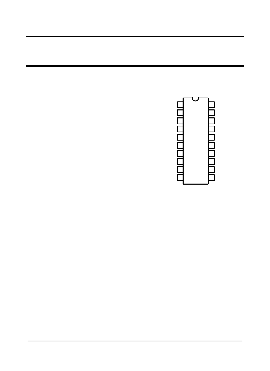
Telephone Speech Network with Dialer Interface
1
2
3
4
5
6
7
8
9
11
16
19
V
TO1
TO0
MFI
TPO
TPI 1
TPI 2
MUTE
GND
RO 1
RO 2
BT 1
RPO
RPI 1
RPI 2
REF
PADC
UP
Description
The GL6965 is a bipolar integrated circuit for
use in electronic telephones.
The GL6965 has low operating voltage, it provides an excellent branch performance.
It has line voltage increasing circuit by the
exter-nal terminal. Transmitting and receiving
gains automatically vary according to the line
current.
Features
• Externally adjustable transmitting,
receiving and Sidetone gains.
• Switching between transmitting output
and DTMF output is possible.
• Direct interface with light and compact
ceramic transmitter-receiver is possible.
• Receiver follow impedance type can
also be used.
GL6965
GL6965
Pin Configurations
AC BIAS
10
• Gain is automatically controlled according to the line current (Auto-PAD
function).
• The line voltage can be increased by
the external terminal (Up function).
• PKG is 20 pin DIP.
V
20
CC
18
17
15
14
13
12
1
Page 2
C
25Ta°=
70
~30
−
150
~55
−
C
°
C
°
C
25Ta°=
1
9
10
2
3
17
16
15
14
13
12
20
11
4
5
6 7 8
18
19
+ +
+
GL6965
Absolute Maximum Ratings (
Parameter Symbol Value Unit
Line Voltage
Line Current
Power Dissipation
Operating Temperature
Storage Temperature
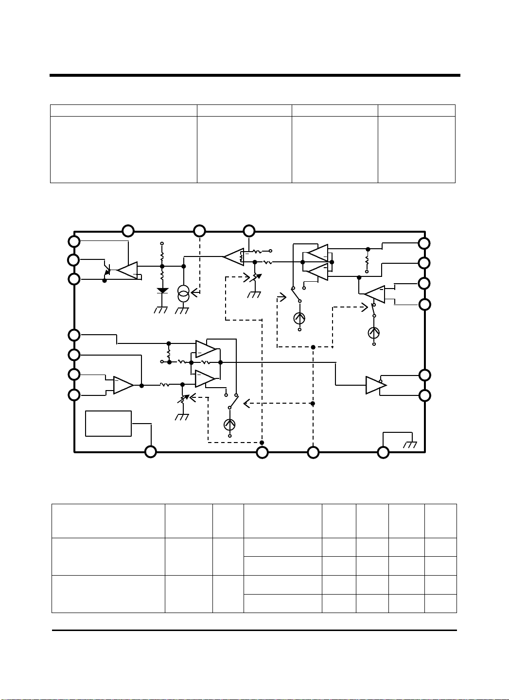
Block Diagram
+
+
RECEIVING
INPUT
AMP
VCC
VCC
10K
9.3K
Vref
REF
5.5K
SW/BUFFERRECEIVING
17.7K
RECEIVING
CONTROLLER
RPI1
RPI2
VL
TOl
TOO
BTI
RPO
LINE DRIVER
INTERNAL
REFERENCE
CIRCUIT
GAIN
Iup
+
AC Bias
+
17.7K
UP
VCC
)
V
L
I
L
P
D
T
opr
T
stg
AMP
4K
TRANSMIT
GAIN
CONTROLLER
AC Bias
Vref
PADC
15
150
1300
TRANSMIT SW/BUFFER
+
VCC
MUTE
27.4K
Vref
VCC
RECEIVING
DRIVE AMP
mA
mW
TRANSMIT
INPUT
AMP
GND
V
MFI
TPO
TPI1
TPI2
RO2
RO1
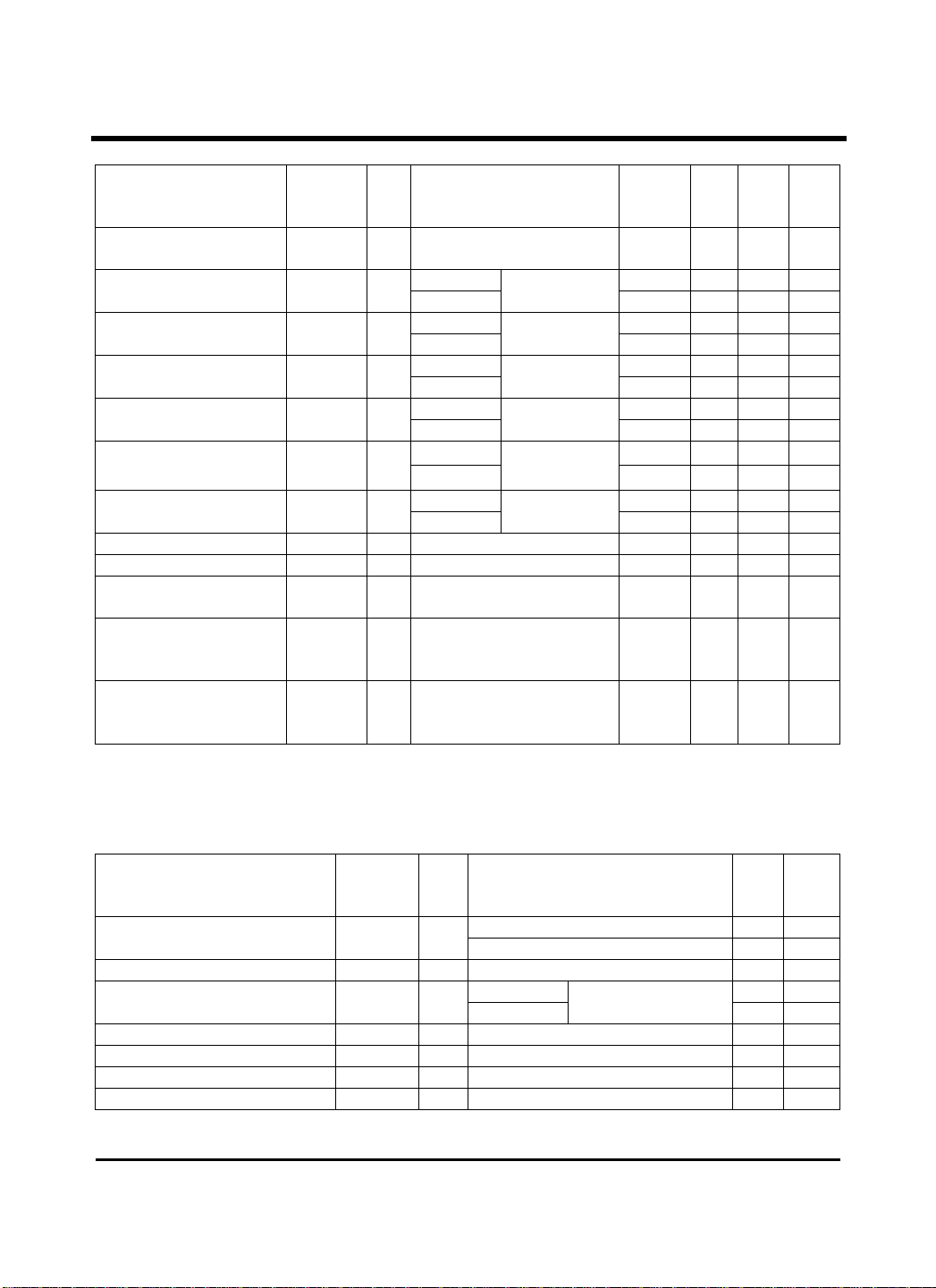
Electrical Characteristics (
Parameter Symbol
)
Test
Cir-
Test Condition Min. Typ. Max. Unit
cuit
IL=20mA 2.9 3.2 3.6 V
Line Voltage
Internal Power Supply
Voltage
V 1
L
V 1
CC
IL=120mA 9 11 14 V
IL=20mA 1.75 1.90 2.20 V
IL=120mA 5.8 6.1 6.6 V
2
Page 3
KHz1f
−
=
KHz1f
−
=
KHz1f
−
=
KHz1f
−
=
Test
Cir-
Test Conditon Min,. Typ. Max. Unit
cuit
Parameter
Line Voltage Rise up
Sym
-bol
V∆ 2 IL=20mA 1.1 1.5
L
Amount
Transmit Gain
Receiving Gain
MF Gain
Beep Gain
Transmit Dynamic Range
Receiving Dynamic Range
G 4
T
G 5
R
G 6
MF
G 8
BP
D 4
RT
D 5
RR
IL=20mA 43 46 48 dB
IL=120mA
IL=20mA 40 43.5 46 dB
IL=120mA
IL=20mA 24 26.8 28 dB
IL=120mA
IL=20mA 21 24 27 dB
IL=120mA
IL=20mA
IL=120mA
IL=20mA 3.0 — —
IL=120mA
=
dBV55V
in
=
dBV55V
in
=
dBV30V
in
=
dBV30V
in
Distortion
Ratio 4%
Distortion
Ratio 10%
MFI Input Resistance ZI(MF) — 21 30
BTI Input Resistance ZI(BP) — 7 10
AC BIAS Input
Resistance
MUTE Terminal High
Level
ZI(AB) —
)MU(V
IH
—
21 30
IL=20mA-120mA
Input Voltage
MUTE Terminal Low
Level
)MU(V
IL
—
IL=20mA-120mA 0 — 0.2 V
Input Voltage
GL6965
2.1
40 43.2 45 dB
34.5 38 40.5 dB
21.5 24 25.5 dB
21.5 24.5 27.5 dB
2.0 — —
4.0 — —
6.0 — —
V -
CC
0.5
—
V
— Ωk
— Ωk
— Ωk
CC
V
V
V
V
V
p.p
p.p
p.p
p.p
V
Reference data
Test
Cir-
Test Condition Typ Unit
cuit
IL=20mA 0.66 V Internal Reference Voltage
3
IL=120mA 2.8 V
RO
R
11
IL=20mA 14.5 dB Total Receiving Gain
IL=120mA
(Balancing Network
circuit included.)
9 IL=20mA VIL=0.2V -50 µA
10 IL=20mA at GND connection -35 µA
9.0 dB
Parameter Symbol
V
REF
RO1, RO2 Output Impedance
Z — IL=30mA f=1KHz 200
G
(Total)
MUTE Terminal Input Current )MU(I
UP Terminal Input Current )MP(I
IL
IL
AC Impedance |Z|TEL — IL=50mA f=1KHZ 580
Phase θ — IL=50mA f=1KHZ 3 DEG
3
Page 4
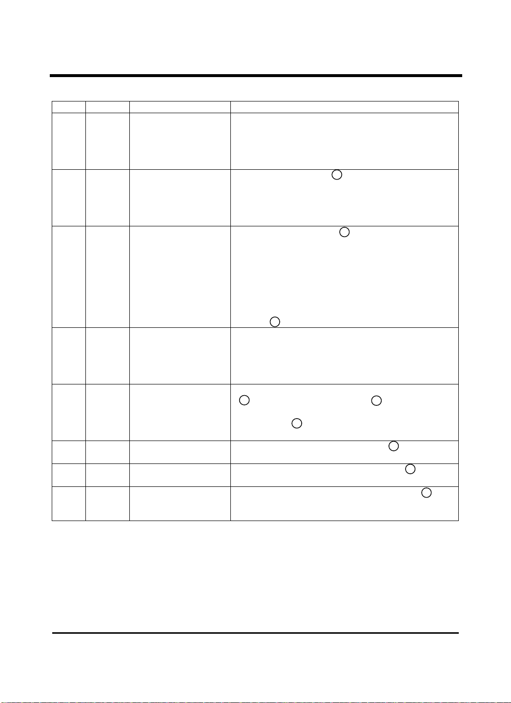
Pin Descriptions
1
1
1
913
7
6
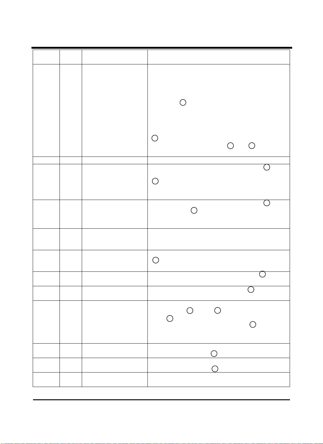
Pin No. Symbol Function Explanation
1 VL Line Current flow-in and
2 TOI Current flow-in terminal
3 TOO Current output terminal
4 AC
5 MFI Input terminal of DTMF
6 TPO Output terminal of
7 TPI1 Inversion input terminal
8 TPI2 Non-inversion input
Bias
Line Voltage terminal
of transmit output
of transmit output
AC signal reference
Voltage terminal
or external input signal
transmit input Amp.
of transmit input Amp.
terminal of transmit input
Amp.
Connected to positive output of diode bridge circuit. DC
potential of this terminal determines line voltage and if AC
signal is not input, the highest DC potential appears.
Transmit output signal and output signal of opposite transfer
side are intermingled and output at this terminal in actual use.
Connected to VL terminal ( pin) through 43 Ω . Since
almost all the line currents flow in from this terminal, set
allowable power of resistance 43 Ω to be connected to VL
terminal from this terminal considering the maximum line
cur-rent expected to be used.
Connected to GND terminal ( pin) through 15 Ω . Since
almost all the line currents flow out from this terminal, set
allowable power of resistance 15 Ω to be connected to GND
terminal from this terminal considering the maximum line
cur-rent expected to be used.
Transmit signal is sent from this terminal. Signal of this terminal varies current which is input from line through connected resistance 15 Ω , and makes it be output at VL
terminal ( pin)
When AC signal is input to this terminal through capacitor
(for blocking DC), signal is sent to line, Input from this terminal is output to line without any relation to gain control
(PAD) or MUTE since this input does not pass through gain
control circuit or MUTE function
Signal which is input to this terminal is output at VL terminal
( pin) only when MUTE terminal ( pin) is in “L” state.
Since this terminal is biased to almost the same potential as
REF terminal ( pin), avoid direct impressing external
DC potential by using capacitor at inputting external terminal.
Makes negative feedback to TPI1 terminal ( pin)
Receives negative feedback from TPO terminal ( pin)
Applies DC bias to this terminal from REF terminal ( pin)
through resistance
GL6965
10
13
4
Page 5
11119 18 10
15 19 18 19 18 93
Pin No. Symbol Function Explanation
9 MUTE
MUTE terminal Switching terminal of transmit signal with MFI input signal
in transmitting system.
Switching terminal of receiving signal with BTI input signal
in receiving system.
“L” State— Signal which is input from MFI is output to
VL terminal ( pin)
Signal which is input from BTI is output to
terminals RO1 and RO2.
“H” or “ OPEN” state
Transmitting input signal is output to VL terminal
( pin). Receiving input signal is
output to terminals RO1 and RO2 ( pin, pin)
This terminal is pulled up by constant-current circuit
10 GND Ground terminal Connected to negative output of diode bridge circuit.
11 UP DC impedance control
terminal
When this terminal is connected to GND terminal ( pin)
directly or through resistance. DC potential of VL terminal
( pin) can be in-creased up to max. 1.5V (TYP.) in the
same line current.
This function has no relation to the state of MUTE terminal.
12 PADC
Pad control terminal When this terminal is connected to GND terminal ( pin)
or
V terminal ( pin) through resistance, operation cur-
CC
20
rent of gain control (Auto-PAD) performed by line current
can be controlled.
13 REF Internal reference voltage
Output terminal
Voltage of this terminal is used as a reference voltage of in-
ternal amplifiers.
Never used this terminal for an external power supply.
14 RPI2 Non-inversion input
terminal
Apply DC bias to this terminal from REF terminal
13
( pin) through resistance.
of receiving Input Amp.
15 RPI1 Inversion Input terminal
Receives negative feedback from RPO terminal ( pin).
of receiving input Amp.
16 RPO Output terminal of
Makes negative feedback to RPI1 terminal ( pin).
Receiving input Amp.
17 BTI Dial confirmation sound
(Beep Tone, DTMF),
monitor
sound input terminal
Signal which is input to this terminal is output to terminals
RO1 and RO2 ( pin and pin) only when MUTE ter-
minal ( pin) is in “L” state. Since this terminal is biased
to about the same potentialas REF terminal ( pin), avoid
direct impressing external DC voltage through capacitor at
in-putting external signal
18 RO2 Receiving output terminal
19 RO1 Receiving output terminal
20
Inversion output
Non-inversion output
V Internal power supply
CC
Output terminal to receiver. Signal of which phase is
negative to RO1 terminal ( pin), is output.
Output terminal to receiver, Signal of which phase is
negative to RO2 terminal ( pin), is output
Power supply of internal amplifiers
voltage terminal
GL6965
10
16
5
Page 6
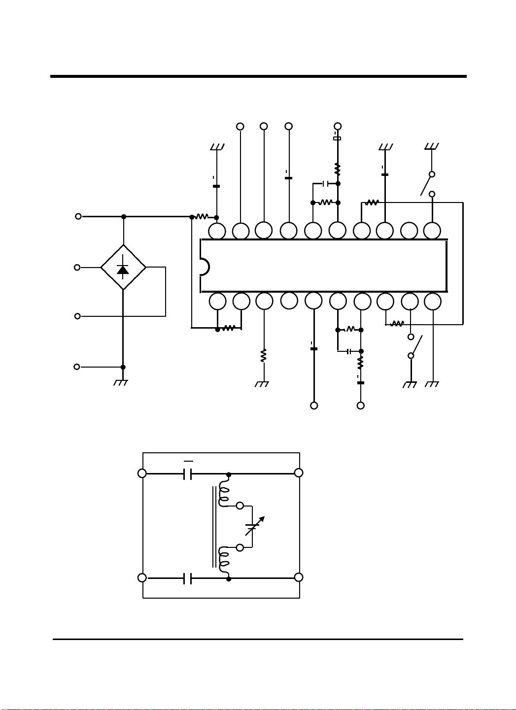
Test Circuit
20
18
15 14 13 12 11
1
3
7 8 9 10
2.2K
+ + + + +
+
–
~
C8
C6
R4
R6
1µF 100
µF µ
2.2KΩ 22KΩ 15Ω 1µ
~
+
–
GL6965
R1 R2 Beep
R2
260
µF
+
19
V
L
L1
L2
2
R1
43
GND
Telephone line Simulation Equivalent circuit
T1
Trunk
2T
2µF
Fì2
Power
C5
330pF
17 16
4 5
DTMF
Line 1
Line 2
R9
22K
R
6
C2
330pF
22K
R5
F
T(+)
R8
2.2K
F
µF
R7
6
Page 7
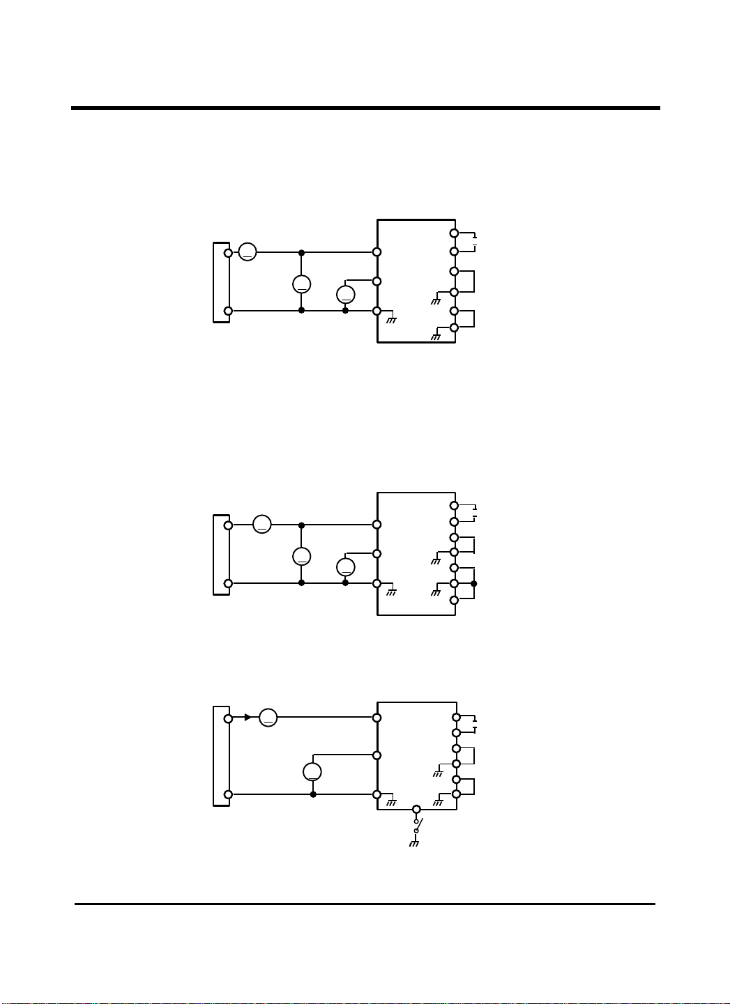
Test Circuit (continued)
V
LLV
CC
V
CC
R
R
LLV
CC
V
CC
R
R
LLVVV R
R
I
UP
1. LV , CCV
2. LV , CCV (UP)
3.
REF
GL6965
A
V
V
A
V
V
A
V
V
V
GND
T(+)
V
V
GND
T(+)
T(+)
SW
55nF
R
55nF
R
55nF
R
7
Page 8

Test Circuit (continued)
LLR
2
R
I
V
A
1
L
Vcc
R
LLV
R
2
R
T(+)
I
V
A
1
L
GND
Vcc
LLV
R
2
R
MF
I
V
A
1
L
GND
Vcc
NUTE
4. TG , TDR
600Ù
T
1
T
2
5. RG , RDR
600Ù
T
1
T
2
6. MFG , MFDR
600Ù
T
1
T
2
V
OUT
PADC
L
2
l Transmit Gain, |V/V|log20=
G (dB)
l Transmit Dynamic Range:
at
V : DIST= 4%
OUT
PADC
L
2
l Receiving Gain, |V/V|log20=
G (dB)
l Receiving Dynamic Range:
at
V : DIST= 10%
OUT
V
OUT
PADC
L
2
l MF Gain, |V/V|log20=
G (dB)
l MF Dynamic Range:
at
V : DIST= 4%
OUT
8
55nF
V
IN
10K
20K
25K
100K
SW
PADC
V
OUT
V
IN
10K
20K
25K
100K
SW
PADC
V=DR (Vp-p)
55nF
V
IN
10K
20K
25K
100K
SW
PADC
INOUTMF
V=DR (Vp-p)
OUTMF
GL6965
INOUTT
V=DR (Vp-p)
OUTT
INOUTR
OUTR
Page 9

Test Circuit (continued)
LLR
L
2
R
T
T
V
V
LLR
2
R
I
V
A
1
L
Beep
LLR
R
I
L
L
IN
7. RG , RDR (at RL=150Ω; Low Impedance Type Receiver)
600Ù
A
I
L
R
GND
L
4.7µF
l Receiving Gain, (dB)
l Receiving Dynamic Range: -p)
at
V : DIST= 10%
OUT
8. BPG , BPDR
600Ù
T
1
T
2
MUTE
L
2
l Beep Gain, |V/V|log20=
l Beep Dynamic Range:
at
G (dB)
V : DIST= 10%
OUT
9. ILG (MU)
A
R
T
IN
MUTE
I (MU)
IL
510Ω
150Ω
0.022µF
Insertion is required at oscillation
A
V
V
OUT
V
IN
INOUTBP
V=DR (Vp-p)
OUTBP
55nF
0.2V
GL6965
9
Page 10

Test Circuit (continued)
LLR
R
I
L
L
INTIN
LLRIL
L
2
R
55nF
V
OUT
V
V
10. ILI (UP)
11. RG (Total)
T
1
IN
T
2
A
A
l Total Receiving Gain, |V/V|log20=)Total(
*Balancing circuit included
GL6965
55nF
R
A
I (UP)
UP
G (dB)
IL
INOUTR
10
Page 11

R8 2.2K
GL6965 Block Diagram & Application Circuit
VCC
AC Bias
TPO
VL TOI TOO BTI RPO RPI1 RPI2 REF PADC MUTE GND
14
17
3 2 1
8
7
6
5
18
19
4
11
20 12
10
9
REFERENCE
CIRCUIT
RECEIVING
CONTROLLER
TRANSMIT
CONTROLLER
TRANSMIT
INPUT
AMP
RECEIVING
INPUT
AMP
RECEIVING S
SW/BUFFER
RECEIVING
DRIVER
AMP
R
T
LINE
BALANCING
NETWORK
R103 6.2K C101 0.01 R101 1.5K R102 11K R3 150 R4 15/1W
C5 330P R10 2.2K 22K C6 0.47 BEEP TONE
C4 100/25V
43/1W R1 LINE DRIVER
R2 620
SW(UP) VCC 10K 5.5K lup AC Bias AMP VCC 17.7K 17.7K 9.3K
Vref 4K VCC VCC
SW/BUFFER
TRANSMIT
27.4K
RECEIVER
R5 22K C3 330P R6 2.2K C3 0.47 C1 0.1 DTMF R7 2..2K SW (MUTE)
+
+
+
+
*** UNITS ***
C:
R: Ohm PKG: 20 DIP
GL6965
TRANSMITTER
I2
GAIN
GAIN
INTERNAL
µF
11
Page 12

Gain Distribution
(Externally Adjustable)
0 dB
(At line 600 Ohm
termination)
IL=20mA
IL=120mA
(Externally Adjustable)
0 dB
(Externally Adjustable)
(Externally Adjustable)
IL=20mA
IL=120mA
The Gain value is the one roughly determined
+ ++
BALANGING
NETWORK
*** Receiving Path Gain Distribution ***
R
BEEP TONE
0.1
R9 2.2K
R7 2.2K LINE L1, L2
* * * Unit * * *
C: UF R: Ohm
The Gain value is the one roughly determined
*** Transmit Path Gain Distribution ***
+
+
T
0.47
R1
2.2K
R3
2.2K
TPI1
TPI2
R2
2.2K
TPO
0.1
MF 27.4K AC Bias
VL
R5 43
R5 620 R5 15
* * * Units * * *
C: uF
GL6965
20 dB
Transmit Input Amp.
20 dB
Receiving Input Amp.
Transmit SW/Buffer
Transmit PAD
AC Bias Amp.
26 dB
Line Drive Amp.
0 dB
Receiving SW/Buffer
0 dB
-3 dB
0 dB
-5.5 dB
Receiving PAD
20 dB
Receiving Input Amp.
- 29 dB
Balancing Network
12
Page 13

GL6965
PIN20 (UP)
10k
5 k
1.5
0.015µF
10 kΩ
2.0 k§Ù
6.2 k§Ù
Description Functions
1. Line voltage increasing circuit (up)
The voltage of VL,VCC or V
can be increased by connecting UP terminal to GND directly or
REF
through the resistance.
The internal equivalent circuit is as shown in the figure.
(1) The voltage increased most up to about 1.5V in VL when UP terminal is directly connected to
GND. when the resistance is inserted the voltage increases according to the resistance value.
(See graph)
(2) In case of usage with MUTE terminal connected, the line voltage can be increased only at
muting.
(3) Avoid impressing the voltage over VCC or under GND.
(4) When not in use, make the circuit opened or connected to V
CC.
Internal equivalent circuit
PIN20 (VCC)
l
UP
2. Side tone protection circuit (Balancing circuit)
The time constant (hereafter referred to as BN constant) of the side tone protection circuit in the
example of application circuit is adjusted nearly to 0.4φ 7dB. Since the side tone characteristic
varies according to this BN time constant, adjust the time constant confirming to the function of the
telephone set.
EXAMPLE OF BN TIME CONSTANT
In case of 0.5φ7dB is determined
to be the center.
13
Page 14

GL6965
20 k§Ù
5 k§Ù
PIN20(VCC)
PIN12 (PADC)
PIN 20 (V
)
Dialing Mode (High)
3. Gain control circuit (PADC)
1) PADC terminal open state. Transmiting and receiving gains vary automatically according to the
line current amount (Auto-PAD). With the increase of line current amount; the gain attenuates by
about - 3dB at transmiting and about - 5.5dB at receiving.
2) In case PADC terminal is connected to GND by resistance. The gain begins to attenuate with the
line current amount less than that when PADC terminal is open. Set the value of resistance to be
connected at 25k§Ùor over.
3) In case PADC terminal is connected to VCC by resistance. The gain begins to attenuate with the
line current amount more than that when PADC terminal is open.
Set the value of resistance to be connected at 10k§Ù or over.
*
Internal equivalent circuit.
4. MUTE circuit (MUTE)
The internal equivalent circuit in the MUTE terminal is a shown in the figure below. Since the
protective diode is connected between VCC and GND, avoid impressing the voltage over that of VCC
or below GND.
This is most suitable for input from the output of open drain or open collector type.
*
Internal equivalent circuit.
I
PAD
PIN9 (MUTE)
V
REF
+
-
Speech Mode (High)
14
Page 15

Application
Ceramic type; The receiver of equivalent capacity of about 55nF is assumed. In case of
EXAMPLE OF CONNECTION CIRCUIT OF
18
510Ω
*
0.022
19
R
Insert at oscillation
- + 1µ
T
560
0.47µF
§Ù
INPUT
1. Transmitter
As the transmitter, ¨ç the condenser microphone. ¨è the ceramic type and ¨é the dynamic type
(speaker type) are available. However, since ¨ç and ¨è of FET or transistor built-in require the
bias circuit. Externally provide the bias circuit. For example, refer to the example of the application
circuit.
2. Receiver
As the receiver, ¨çthe ceramic type ¨è the low-impedance (dynamic type) are available.
(1)
the ceramic type, since the large voltage amplitude is generally required
at driving, make the receiver function in BTL mode.
(2) Low-impedance type; The receiver of equivalent resistance of about 150§Ù is assumed. For the
connections, refer to the example of application circuit.
3. Example of Application circuit.
(1) EXAMPLE OF POWER SUPPLY CIRCUIT
FOR CONDENSER MICROPHONE
V
CC
Ω
TO MICROPHONE
(3) In case of using transmit input amplifier as
non-inversion input.
TRANSMIT INPUT AMP
_
+
6
2.2k§Ù
7
2.2k§Ù
330pF
2.2k§Ù
0.47mF
TRANSMITER
TO 13 PIN
Note : In test circuit and application circuit, transmit
input amplifier is set at inversion input.
1mF
GL6965
(2)
LOW-IMPEDANCE TYPE RECEIVER.
+ -
4.7µF
TYPE RECEIVER
F
µF
*
(4) In case of using transmit input amplifier as in-
version input.
6
2.2k§Ù
_
7
T 8
TRANSMIT INPUT AMP
+
8
2.2k§Ù
TO 13 PIN
15
LOW-
IMPEDANCE
(150Ω)
330pF
2.2k§Ù
0.47mF
T
TRANSMITER
Page 16

4. Side Tone Gain Control.
V
19 18
3 2
10 16
L2
220µF
~
~
(1) Alternative application for side tone gin control
VL
+
L1
-
B/L
Circuit
150Ω
620Ω
0.47µF
20
1
43 Ω
2.2kΩ
GL6965
15Ω
330pF
2.2kΩ
2.2kΩ
0.47µF
15
7
TIN
0.47µF
V
VRD
- The side tone gain is externally controlled by the resistor RSD (RS1+RS2)
- The maximum available control range of side tone gain is 0dB to 14 dB.
(2) Side tone gain, GSD to Resistor, RSD
RS2
RS1
GL6965
5.6kΩ
R
1 kΩ
SD
RSD (RS1+RS2) GSD
1k§Ù
2k§Ù
3k§Ù
3.5k§Ù
4k§Ù
5k§Ù
6k§Ù
14.2dB
11.1dB
2.5dB
0.2dB
1.6 dB
5.4 dB
7.5 dB
(3) The side tone gain is
V
GSD=
RO
log(20
L
)dB()
16
Page 17

5. AC Impedance UP control.
3 2
20
(100k
500k
C
(1) Application for AC impedance up control
VL
R1
43¥Ø
ZAC
- The AC Impedance (ZAC) can be increased by using AC Bias terminal (Pin ¨ê).
- The AC Impedance up amount is determined by the external resistors R1, R2 value. :
(2) The AC impedance is
1
1
(
R
Z
AC
¡Ö
VL
IL
¡Ö
1
R
R2
620¥Ø
1
+
C8
220 µF
- 1
R4
15¥Ø
R
)
R+R
2A1A2A42
4
0.1µF
¥Ø)
R
A1
¥Ø-
R
A2
GL6965
17
Page 18

0 20 40 60 80 100 120 140
4
0 20 40 60 80 100 120 140
48
Transmit Gain(dB)
(A)
(B)
(C)
(E)
(D)
DC Voltage
0 20 40 60 80 100 120
16
0 20 40 60 80 100 120
16
DC Voltage
DC Characteristic (Normal)
Test Circuit 1
14
12
10
8
V
L
6
4
2
Line Current, IL (mA)
V
Voltage to Current Characteristic
REF
Test Circuit 3
3.5
3
2.5
Up
2
1.5
Normal
1
0.5
Line Current, IL (mA)
GL6965
DC Characteristic (UP)
Test Circuit 2
14
12
10
8
V
CC
6
4
2
V
L
V
CC
Line Current, IL (mA)
Transmit Gain to Current Characteristic
Test Circuit 4
47
46
45
44
43
42
41
Line Current, IL (mA)
18
(A) open
(B) 10k§Ù (PADC-VCC)
(C) 20k§Ù (PADC-VCC)
(D) 25k§Ù (PADC-GND)
(E) 100k§Ù(PADC-GND)
Page 19

Receiving Gain to Current Characteristic
0 20 40 60 80 100 120 140
50
Receiving Gain(dB)
(A)
(B)
(C)
(D)
(E)
0 20 40 60 80 100 120 140
29
MF Gain (dB)
(A)
(D)
(E)
(B)
(C)
0 20 40 60 80 100 120 140
30
Beep Gain (dB)
Input Level = -
0 20 40 60 80 100 120 140
26
Receiving Gain (dB)
Input Level = -
R
=150§Ù
Input=pin 15, -55dBV
Output=pin 18, pin 19
Test Circuit 5
48
46
44
Input Level=-55dBV
(K) open
(L) 10k§Ù (PADC-VCC)
(M) 20k§Ù (PADC-VCC)
(N) 25k§Ù (PADC-GND)
(O) 100k§Ù (PADC-GND)
42
40
38
36
Line Current, IL (mA)
Beep Gain to Current Characteristic
Test Circuit 8
28
26
24
22
20
18
16
Line Current, IL (mA)
30dBV
GL6965
MF Gain to Current Characteristic
Input=pin 15, -30dBVrms
Output=pin 1
Test Circuit 6
28
27
26
25
24
23
22
Input Level=-30dBV
(F) open
(G) 10k§Ù (PADC-VCC)
(H) 20k§Ù (PADC-VCC)
(I) 25k§Ù (PADC-GND)
(J) 100k§Ù (PADC-GND)
Line Current, IL (mA)
Receiving Gain to Current Characteristic
(at using Low-impedance type receiver ;
RL=150§Ù)
Test Circuit 7
24
22
20
18
16
14
12
Line Current, IL (mA)
19
55dBV
Page 20

0 20 40 60 80 100 120 140
0 20 40 60 80 100 120 140
16
Transmit Dynamic Range (Vp
THD 4%
THD 2%
16
Receiving Dynamic Range (Vp
THD10%
THD 5%
0 20 40 60 80 100 120 140
16
MF Dynamic Range (Vp
THD 4%
THD 2%
0 20 40 60 80 100 120 140
16
Beep Dynamic Range (Vp
THD10%
THD 5%
Transmit Dynamic Range to Current Characteristic Receiving Range to Current Characteristic
-p)
14
Test Circuit 4
12
10
8
6
4
2
Line Current, IL (mA)
DTMF Dynamic Range to Current Characteristic Beep Dynamic Range to Current Charcteristic
14
-p)
12
Test Circuit 6
10
8
6
4
2
Line Current, I
GL6965
Test Circuit 5
-p)
14
12
10
8
6
4
2
Line Current, IL (mA)
Test Circuit 8
14
-p)
12
10
8
6
4
2
L
Line Current, IL (mA)
20
Page 21

0 20 40 60 80 100 120
1.6
Dynamic Range (Vp
THD10%
THD 5%
0 20 40 60 80 100 120
19
Total Receivin
Gain
AC Impedance
700
GL6965
Receiving Dynamic Range to Current Characteristic
At using Low-Impedance type Receiver ; RL=150
Test Circuit 7
-
1.4
1.2
1.0
0.8
0.6
0.4
0.2
Line Current, IL (mA)
AC Impedance to Frequency Characteristic (IL = 120 mA)
600
500
100 5k
§Ù
Frequency (Hz)
Total Receiving Gain to Current Characteristic
(Balancing circuit included)
Test Circuit 11
17
15
13
g
11
9
7
5
Line Current, IL (mA)
21
Page 22

0 20 40 60 80 100 120 140
Current Value (ìA)
=20mA
Line Voltage V
5.0
Mute Terminal pull-up current characteristic
14
0
12
0
10
0
80
60
40
20
Line Voltage Rise up Characteristic
4.6
(V)
L
4.2
3.8
3.4
3.0
Resistance between up terminal and GND terminal (§Ù)
Test Circuit 9
Line Current, IL (mA)
Test Circuit 2
22
at VIL= 0.2V
I
L
GL6965
Page 23

Transmit Gain to Frequency Characteristic
50
Transmit Gain (dB)
Gain
0 20 40 60 80 100 120
16
DC Voltage (V)
0 20 40 60 80 100 120
16
DC Voltage (V)
Test Circuit 4
45
40
35
100 1k 5k
IL=120mA
IL=120mA
Frequency (Hz)
Receiving gain to Frequency Characteristic
Test Circuit 5
IL=120mA
IL=120mA
100 1k 5k
Frequency (Hz)
GL6965
Input Level=-55dBV
Input Level=-55dBV
Line Voltage to Temperature Characteristic Internal Power Supply Voltage to Temperature
Test Circuit 1
14
12
10
8
6
4
2
Line Current, IL (mA)
-35¡É
75¡É
100¡É
Characteristic
Test Circuit 1
14
12
10
8
6
4
2
23
Line Current, IL (mA)
-35¡É
75¡É
100¡É
 Loading...