

Page 1
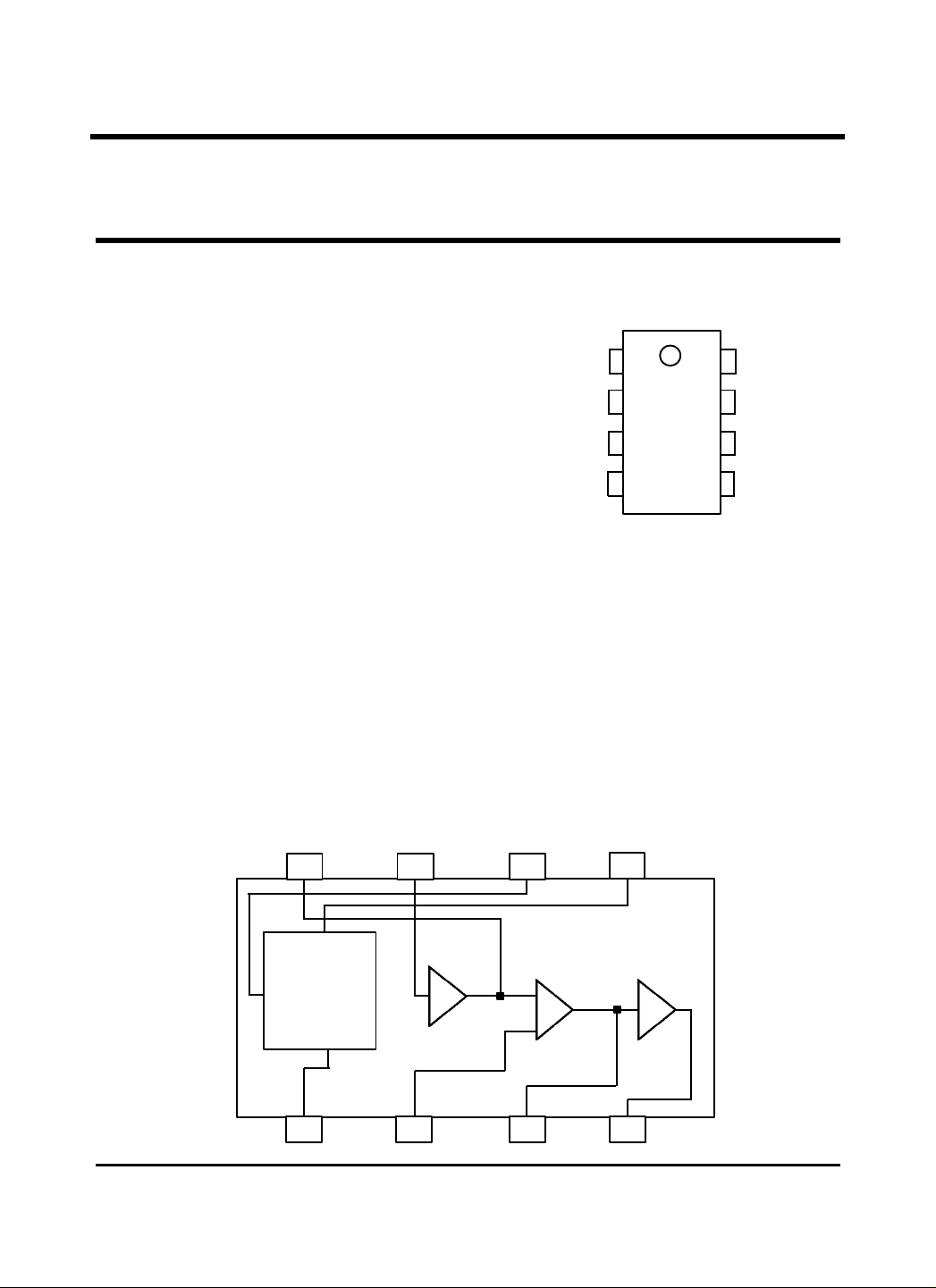
GL6850
1
1 2 3 4 5 6 7
8
VCC
TRIG_IN
LOWOSC_1
LOWOSC_2
OUTPUT
HIGHOSC_2
HIGHOSC_1
GND
6 7 8 4 3
LOW FREQUENCY
HIGH FREQUENCY
OUTPUT
GL6850
TWO TONE RINGER
Description
The GL6850 tone ringer is a monolithic device,
which incorporates two oscillators, and output
amplifier and a power supply control circuit. The
oscillator frequencies can be adjusted over a wide
range by selection of external components. One
oscillator, normally operated at a low frequency,
causes the second oscillator to alternate between its
nominal frequency and a related higher frequency. The
resulting output is a distinct warbling tone. The output
amplifier will drive either a transformer coupled
loudspeaker or a piezo-ceramic transducer.
The device can be powered from a telephone line or
a fixed d.c. supply. The power control circuit has builtin hysteresis to prevent false triggering and rotary dial
chirps. The GL6850 can be triggered externally under
logic control.
Pin Configuration
Features
• Low current consumption.
• Designed for telephone bell replacement.
• Small size MINIDIP package.
• Adjustable 2- frequency tone.
• Built-in hysteresis prevents false triggering and rotary dial CHIRPS.
• Alarms or other alerting devices.
• External triggering or ringer disable.
• Include ESD protection.
GL6850
Block Diagram
POWER SUPPLY
CONTROL CIRCUIT
(WITH HYSTERSIS)
5
OSCILLATOR
2
OSCILLATOR
1
AMPLIFIER
Page 2
2
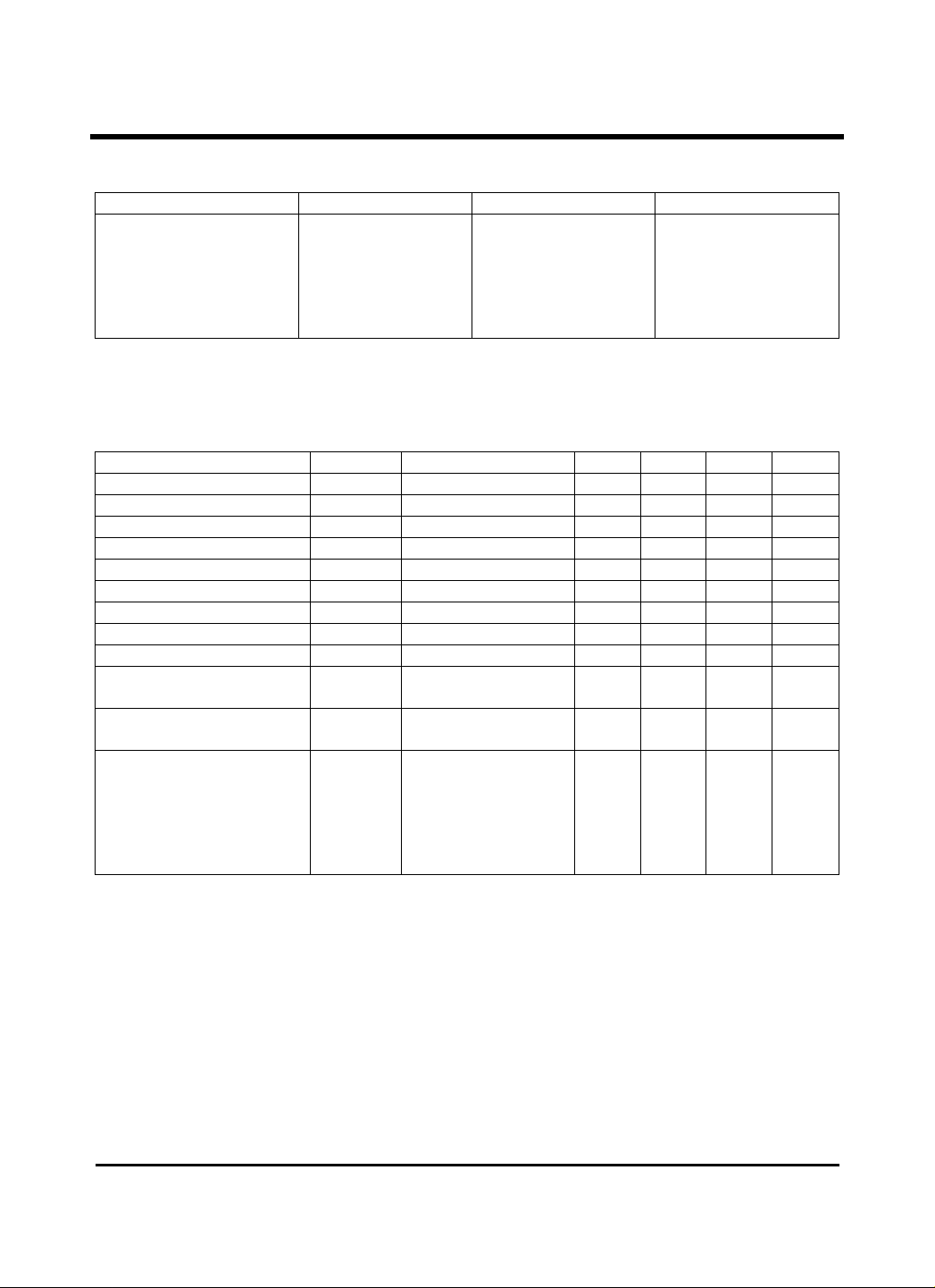
Absolute Maximum Ratings (Ta = 25¡É)
CHARACTERISTICS SYMBOL VALUE UNIT
Supply Voltage
Power Dissipation
Operating Temperature
Storage Temperature
VCC
Po
Topr
Tstg
30
400
-25 to 65
-65 to 150
Electrical Characteristics (Ta = 25¡É)
GL6850
V
mW
¡É
¡É
CHARACTERISTICS SYMBOL TEST CONDITION MIN TYP MAX UNIT
Operating Supply Voltage V
Initiation Supply Voltage
Initiation Supply Current
Sustaining Voltage
Sustaining Current
Trigger Voltage
Trigger Current
Disable Voltage
Disable Current
2
2
3
3
4
4
Output Voltage High V
Output Voltage Low V
High Frequency 1
High Frequency 2
Low Frequency
* NOTE
1. Initial supply voltage (VSI) is the supply voltage required to start the tone ringer oscillation.
2. Sustaining voltage (V
3. VTR and ITR are the conditions applied to trigger to start for V
4. V
DIS
and I
DIS
5. Trigger current must be limited to this value externally.
1
1
CC
V
SI
I
SI
V
SUS
I
SUS
V
TR
I
TR
V
DIS
I
DIS
V
OH
OL
f
H1
f
H2
f
L
) in the supply voltage required to maintain oscillation.
SUS
CC
Pin6 =6V,Pin7=GND
V
CC
Pin6= GND,Pin7=6V
R3=191K, C3=6800Pf
R3=191K, C3=6800pF
R2=165K, C2=0.47µF
- - 29.0 V
17 19 21 V
0.9 2.0 3.7 mA
9.7 11.0 12.0 V
0.4 1.0 2.0 mA
V
= 15 V 9.5 - - V
CC
V
= 15 V 40 - 1000
CC
V
= 21 V - - 0.8 V
CC
V
= 21 V -50 - - µA
CC
=21V, I8=-10mA
=21V, I8= -10mA
17 19 21 V
- - 2 V
461
576
9.0
¡ÂVCC¡ÂVSI
SUS
461
640
10
are the conditions applied to trigger to inhibit oscillation for VSI¡Â VCC
5
563
704
11.0
µA
Hz
Hz
Hz
Page 3

3
PIN DESCRIPTION
100K-200K
TIP
C1
R1
RING
R2
C5
C3
15K
D1 = 29 V ZD
R3 = 191 kohm
1 2 3 4 5
7
8
PIN NUMBER PIN FUNCTION DESCRIPTION
PIN 1 VCC Operating supply D.C. voltage rectified from ringing signal.
Oscillator External Trigger/Inhibit pin (must beconnected through
PIN2 TRIG_IN
a current limiting resistor, which is used to program the slope of
supply current vs voltage.)
PIN3 LOWOSC_1
PIN 4 LOWOSC_2
Low Frequency Time Constant Adjustment pins fL is controlled
externally by R2 and C2
fL = 1/1.289R2C2
PIN 5 GND Ground
PIN 6 HIGHOSC_1
PIN 7 HIGHOSC_2
High Frequency Time Constant Adjustment Pins fH1 and fH2 are
controlled externally by R3 and C3.
fH1=1/1.504R3C3, f
PIN 8 OUTPUT Tone output
APPLICATON CIRCUIT
= 1/1.203R3C3
H2
GL6850
C1 = 0.9uF
C2 = 0.47uF
C3 = 6.8nF
C4 = 22uF / 35V
C5 = 0.22uF
C4
R1 = 560 ohm
R2 = 165 kohm
D1
C2
GL 6850
10K
VOLUME
R3
6
1300 : 8 ohm
 Loading...